Science and applications of wafer-scale crystalline carbon nanotube films prepared through controlled vacuum filtration
Abstract
Carbon nanotubes (CNTs) make an ideal one-dimensional (1D) material platform for the exploration of exotic physical phenomena under extremely strong quantum confinement. The 1D character of electrons, phonons and excitons in individual CNTs features extraordinary electronic, thermal and optical properties. Since the first discovery, they have been continuing to attract interest in various disciplines, including chemistry, materials science, physics, and engineering. However, the macroscopic manifestation of such properties is still limited, despite significant efforts for decades. Recently, a controlled vacuum filtration method has been developed for the preparation of wafer-scale films of crystalline chirality-enriched CNTs, and such films immediately enable exciting new fundamental studies and applications. In this review, we will first discuss the controlled vacuum filtration technique, and then summarize recent discoveries in optical spectroscopy studies and optoelectronic device applications using films prepared by this technique.
I Introduction
Carbon is a fundamental element in Group IV of the periodic table of elements, which is not only essential for life on earth but also promising for modern technologies in communication, computation, imaging, sensing, energy, health and space. Each carbon atom has six electrons, occupying the 1, 2, and 2 atomic orbitals. Two core electrons (1) are strongly bound, while four weakly bound electrons (22) can form covalent bonds in carbon materials using ( = 1, 2, 3) hybrid orbitals. Other Group IV elements like Si and Ge can only exhibit hybridization DresselhuasEtAl2008 . Various hybridization states in carbon lead to a versatile chemical nature and determine the properties of carbon allotropes and organic compounds HirschEtAl2010NM . Two natural carbon allotropes, diamond and graphite with and hybridization, respectively, show distinct properties; they were the only known carbon allotropes for a long time until the discovery of zero-dimensional (0D) C60 in 1985 KrotoEtAl1985N , giving birth to nanotechnology. After the advent of C60, a growing family of carbon nanomaterials emerged, including 1D carbon nanotubes (CNTs) IijimaEtAl1991N and two-dimensional (2D) graphene NovoselovEtAl2004S . Still other members, based on numerous combinations and modifications of carbon atom hybridization, are yet to be discovered. Despite the unique properties of each member of the carbon nanomaterial family, their atomic structures are related to one another. In this sense, graphene can be viewed as a fundamental building block because fullerenes, carbon nanotubes, and graphite can all be derived from graphene GeimEtAl2007NM . In particular, a single-wall CNT (SWCNT) is a rolled-up version of monolayer graphene, which possesses unique 1D thermal, mechanical, electronic and optical properties DresselhuasEtAl2008 ; AvourisEtAl2008NP ; NanotEtAl2012AM ; NanotEtAl2013 .
I.1 Electronic, optical properties and applications of SWCNTs
The crystal and band structure of SWCNTs are highly related to those of graphene. However, the strong confinement of electronic states along the tube circumference makes SWCNTs a completely different material. Graphene consists of a hexagonal lattice of -bonded carbon atoms, as shown in Figure 1(a). The carbon-carbon bond length is 1.42 Å. The primitive unit cell contains two carbon atoms, A and B, contributing two electrons that play fundamental roles in electrical and optical phenomena. Figure 1(b) shows the reciprocal lattice of graphene, which is also a hexagonal lattice, and there are three important high-symmetry points: -point (the center of the Brillouin zone), -point, and -point. The and are the primitive unit vectors in real and reciprocal space, respectively.
The band structure of SWCNTs sensitively depends on the manner in which the graphene sheet is rolled up, which can be uniquely specified by defining the chiral vector , where and are positive integers with ; see Figure 1(c). A SWCNT is formed by wrapping the graphene sheet in such a way that the two points connected by C meet, with a diameter . The chiral indices (,) fully determine the crystal structure of the SWCNT and the character of the band structure depends on the value mod 3:
1. If , the SWCNT is metallic;
2. If or 2, the SWCNT is semiconducting with a band gap 0.7 eV/ (nm).
However, due to the nanotube curvature effect, only armchair nanotubes () are truly metallic. For other tubes with , there is a small, curvature-induced band gap that scales with 1/.
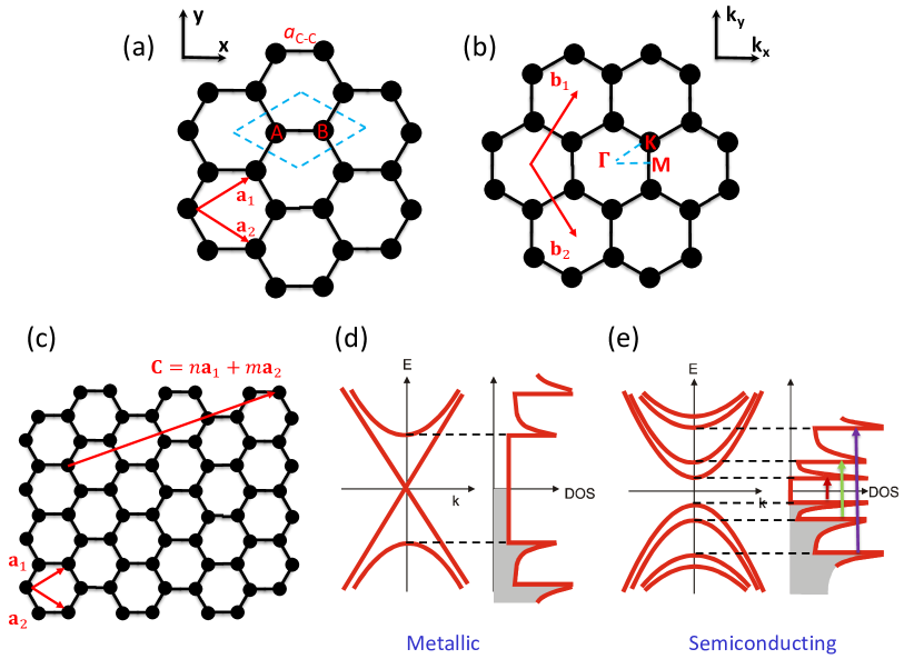
As shown in Figures 1(d) and 1(e), 1D SWCNTs have a divergent density of states at the van Hove singularities, which, together with strong 1D excitonic effects, produces strong optical absorption and emission through the excitation and recombination of electron-hole pairs. The strong quantum confinement of electron-hole pairs results in the generation of stable excitons, and these excitons can be excited either optically or electrically and their radiative recombination results in photoluminescence or electroluminescence, respectively. On the other hand, the 1D nature of SWCNTs limits the direction of carrier scattering to occur only along the nanotube axis while in a higher dimensional material system, scattering directions can be arbitrary. For example, metallic SWCNTs have a limited momentum space, resulting in a suppression of back scattering and a very long mean free path AndoEtAl1998JPSJ , which is ideal for quantum wire interconnections TansEtAl1997N . Furthermore, field effect transistors built from semiconducting SWCNTs have demonstrated a strong electric field effect and showed an extremely high room temperature mobility 105 cm2/Vs DurkopEtAl2004NL . In addition, the optical absorption of semiconducting SWCNTs can be electrically modulated, laying the foundation for optoelectronic device applications.
Although individual CNTs provide an ideal platform for investigating fundamental properties of CNTs and demonstrating proof-of-concept optoelectronic device applications, individual SWCNT devices are still problematic from the viewpoint of practical applications because of a complicated fabrication process, low photoluminescence quantum yields, and an inability to scale up ParkEtAl2013N . Individual CNT transistors are considered to be impractical due to difficulty in positioning CNTs precisely, which applies to individual CNT photonic and optoelectronic devices as well. Although light-matter interaction in individual CNTs is unusually strong, further cooperative enhancement can be expected when a large number of CNTs can be assembled in an ordered manner.
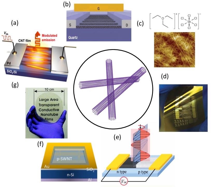
The macroscopic assembly of individual CNTs, in the form of random networks or aligned arrays, is the key to facilitating practical applications. An ensemble assembly can help overcome challenges in individual CNT devices by (1) minimizing device variations, (2) providing a large active area, and (3) not requiring precise individual tube positioning. Currently, there are various ways to prepare a CNT ensemble, including chemical vapor deposition (CVD) MurakamiEtAl2004CPL ; KocabasEtAl2005S and solution-based deposition MeitlEtAl2004NL . The produced ensemble can exhibit either a semiconducting or metallic material behavior and has spurred a wide interest in various applications. For example, CNTs are thermally and chemically stable BegtrupEtAl2007pssb , making them ideal for high-temperature emitters MoriEtAl2014NL (Figure 2(a)) and compatible with high- material deposition for high-performance electronics KangEtAl2007NN (Figure 2(b)). A large ratio of the surface area to the volume of CNTs enables an efficient charge transfer doping from surrounding chemicals for optimized thermoelectric materials AveryEtAl2016NE (Figure 2(c)). The excellent mechanical strength of CNTs is perfect for large-area flexible electronic/optoelectronic applicationsCaoEtAl2008N (Figure 2(d)). Large active areas possess the potential for an efficient broadband detector HeEtAl2013N ; HeEtAl2015AOM (Figure 2(e)) and enable low-cost, high-efficiency heterogeneous solar cells JungEtAl2012NL (Figure 2(f)). Furthermore, a highly conductive metallic SWCNT thin film of a small optical absorption cross section with strong mechanical properties can serve as a stretchable transparent electrode, which is important for certain security applications and backlit displays WuEtAl2004S (Figure 2(g)).
To best preserve the extraordinary properties of individual CNTs, macroscopic ensembles with a single domain of perfectly aligned CNTs, i.e., crystalline CNTs, is highly preferred. Taking SWCNT transistors, for example, the composition and morphology of conducting channels strongly affect the device performance. The degree of SWCNT alignment and the purification of semiconducting SWCNTs affect two important device parameters: the carrier mobility and the on-off ratio RouhiEtAl2011N . With a perfectly aligned semiconducting SWCNT ensemble, the mobility and on-off ratio of a large-scale transistor are comparable with transistor devices based on individual CNTs. In contrast, a randomly oriented ensemble leads to a decrease in mobility that is due to stronger intertube scattering ParkEtAl2013N . Furthermore, even a small amount of metallic nanotubes (e.g., 1%) dramatically decreases the on-off ratio (e.g., three orders) because of the percolation path formed by metallic tubes SarkerEtAl2011N . Therefore, it is crucial to separate nanotubes by electronic types and assemble them in an ordered manner to extend the excellent properties of individual CNTs to CNT macroscopic ensembles for real-world applications.
I.2 Challenges in synthesis of wafer-scale crystalline CNTs
To date, it is still challenging to produce a macroscopic single-domain, highly aligned, densely packed, and chirality-enriched SWCNT film. Current assembly techniques can be separated into two general categories: (1) in-situ direct-growth assembly methods and (2) ex-situ post-growth assembly methods. However, techniques in both categories have inherent limitations.
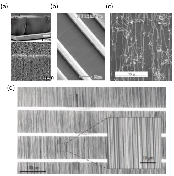
Direct-growth assembly methods mainly consist of the CVD growth method for either vertical MurakamiEtAl2003CPL ; MurakamiEtAl2004CPL ; HataEtAl2004S ; PintEtAl2009JPC or horizontal alignment JoselevichEtAl2007 with respect to growth substrates. If the catalyst density is high enough, a crowding effect leads to vertical alignment of CNTs with heights of mm, as shown in Figure 3(a). The as-grown patterns of well-aligned SWCNTs synthesized using the CVD method can be laid over to form horizontally aligned patterns and be transferred to any substrates through a scalable, facile, and dry approach PintEtAl2010N . To directly assemble horizontally aligned arrays of CNTs, multiple external-stimuli-assisted CVD growth methods have been developed, including electric field ZhangEtAl2001APL , gas flow HuangEtAl2003JPC and epitaxy KangEtAl2007NN . Electric fields can orient CNTs because of the large and highly anisotropic polarizability of CNTs (Figure 3(b)); a feeding gas flow can generate a flow field that can carry CNTs to overcome the gravity to grow along the flow direction (Figure 3(c)); and the oriented van der Waals force along the substrate surface can produce horizontally aligned CNTs (Figure 3(d)).
However, there is a common issue for direct-growth methods: it is still very challenging to control the chirality during the growth procedure. Obtained aligned arrays have mixed electronic types and are not desirable for most applications. Recently, there have been breakthroughs in precisely controlling chirality distribution during synthesis, by designing a catalyst that matches the carbon atom arrangement around the nanotube circumference of a specific chirality YangEtAl2014N ; Sanchez-ValenciaEtAl2014N ; ZhangEtAl2017N . However, the packing density of aligned arrays is relatively low. The highest density reported is 50 CNTs/m DingEtAl2008JACS , which is quite dilute in a practical sense, especially for photonic and optoelectronic applications.
Post-growth assembly methods mainly consist of solution-based techniques for CNT alignment DruzhininaEtAl2011AM . It can take advantage of solution-based SWCNT separation techniques, such as the DNA-wrapping method ZhengEtAl2003S ; TuEtAl2009N , the polymer-wrapping method NishEtAl2007NN , density gradient ultracentrifugation ArnoldEtAl2006NN ; GhoshEtAl2010NN , gel chromatography LiuEtAl2011NC , and aqueous two phase extraction KhripinEtAl2013JACS ; FaganEtAl2014AM . Existing post-growth assembly techniques consist of methods using external force, self-assembly and liquid crystal phase transition.
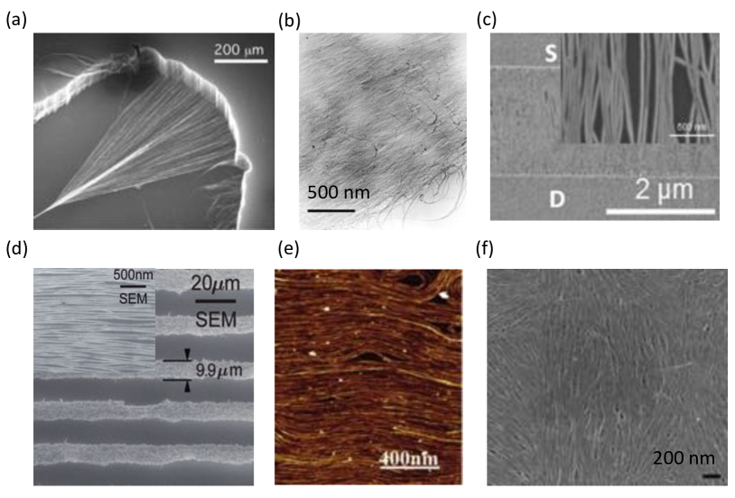
External forces used in CNT alignment can be mechanical, magnetic, and electrical. The simplest method is based on mechanical force by dry-spinning CNTs from a CVD-grown CNT forest (Figure 4(a)) ZhangEtAl2004S ; however there is no chirality selectivity in this method. An applied magnetic field can align CNTs based on their magnetic susceptibility anisotropy, but the required magnetic field to achieve meaningful alignment (Figure 4(b)) is typically larger than 10 T SmithEtAl2000APL , impractical for any practical applications. A more affordable and practical method is to align CNTs in liquid by applying an AC electric field, called dielectrophoresis ShekharEtAl2011N , as shown in Figure 4(c). The obtained films have alignment packing densities up to 3050 SWCNTs/m, which is still quite low. Furthermore, the alignment quality is relatively poor and full surface coverage is nearly impossible.
Instead, self-assembly methods, including evaporation-driven self-assembly EngelEtAl2008N ; ShastryEtAl2013S , Langmuir-Blodgett LiEtAl2007JACS and Langmuir-Shaefer CaoEtAl2013NN assembly, can produce a large-size full-surface-coverage aligned film. As the substrate is immersed inside a CNT suspension during the evaporation-driven self-assembly process, the interplay between the surface friction force, liquid surface tension, and capillary force can align CNTs at the solid-liquid-air interface (Figure 4(d)). Similarly, when the immersed substrate is pulled out of the CNT suspension vertically (Langmuir-Blodgett) or horizontally (Langmuir-Shaefer), the 2D confinement at the air-water interface causes CNTs to orient along certain directions (Figure 4(e)). A semiconducting SWCNT aligned monolayer film of an impressively high packing density of 500 CNTs/m with full surface coverage has been demonstrated for significantly improved transistor performance CaoEtAl2013NN . However, the thickness of fabricated films using these techniques is limited to a few nanometers because of the 2D nature of these techniques, and again the degree of alignment is not very high.
In contrast, a liquid crystal phase transition can lead to alignment in three dimensions. One strategy is to mix CNTs with a liquid crystal polymer matrix DierkingEtAl2005JAP ; LagerwallEtAl2008JMC . Under certain conditions, the liquid crystal polymer can go through a phase transition spontaneously with macroscopically ordered structures, where the hosted CNTs follow the same transition. The degree of alignment can be very high, but the challenge is how to remove the liquid crystal polymers completely without destroying the alignment of CNTs. As a consequence, it motivated another strategy to use the liquid crystal transition of CNTs based on Onsager’s theory. Different aqueous dispersion systems have been investigated to achieve nematic ordering of CNTs BadaireEtAl2005AM ; McleanEtAl2006NL ; DanEtAl2012IECR in a short range (Figure 4(f)), but wafer-scale crystalline CNT films through a liquid crystal phase transition has not been achieved.
II Fabrication and characterization of wafer-scale crystalline films of chirality-enriched CNTs
Post-growth assembly methods are suitable for fabricating 3D architectures of macroscopically aligned CNTs, because of the availability of various solution-based chirality separation techniques. However, existing methods suffer from low packing densities, small thicknesses, incompatibility of separation techniques, and local alignment. Currently, there are no available techniques for fabricating large-area multi-domain films of highly aligned, densely packed, and chirality-enriched SWCNTs with controllable thickness. Recently, He and coworkers have developed a new “solution-based” alignment technique based on controlled vacuum filtration HeEtAl2016NN , which can provide a uniform, wafer-scale SWCNT film of an arbitrarily and precisely controllable thickness (from a few nm to 100 nm) with a high degree of alignment (nematic order parameter 1) and packing ( tubes in a cross-sectional area of 1 m2) in a simple, well-controlled, and reproducible manner, regardless of the synthesis method, type, or chirality of the SWCNTs used. Furthermore, the produced films are compatible with standard micro/nanofabrication processes used to fabricate various electronic and photonic devices.
The controlled vacuum filtration process starts with a well-dispersed CNT suspension, where individual CNTs are separated and suspended. In order to prepare an aqueous suspension, the sidewalls of SWCNTs have to be functionalized either by chemical functional groups or amphiphiles with a hydrophobic tail and a hydrophilic head MaEtAl2010CPASM . Ultrasonication is a widely used method for general nanoparticle dispersion, agitating molecules either in a bath or probe (or horn) sonicator. The generated ultrasound wave is delivered to a CNT bundle in a surfactant solution, and individual CNTs are peeled off from the outer part of the CNT bundle and wrapped by surfactant molecules to prevent future rebundling. The obtained suspension is then ultracentrifuged to remove any undissolved bundles, and the supernatant is collected. The prepared suspension is poured into a vacuum filtration system, as shown in Figure 5(a). A filter membrane with a pore size smaller than the CNT length blocks the passage of CNTs and allows water to penetrate through, under a differential pressure applied across the membrane that is maintained by a vacuum pump underneath. During the deposition process of CNTs, the penetrability of the filter membrane reduces gradually. This self-limiting process guarantees a uniform film WuEtAl2004S ; see Figure 5(b). The obtained film can be readily transferred onto any substrate, such as a quartz wafer in Figure 5(c), by dissolving the filter membrane in organic solvents. Furthermore, as long as CNTs are well-dispersed in the suspension, the controlled vacuum filtration can apply to any CNT species, enabling us to take advantage of solution-based chirality separation techniques. For example, filtrated films made from mono-dispersed SWCNTs separated using density gradient ultracentrifugation show different colors due to subtractive coloration HarozEtAl2012JACS .
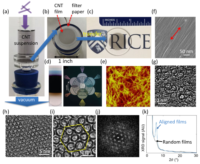
It has been believed that the vacuum filtration technique can only produce randomly oriented CNTs for many years. Figure 5(e) demonstrates an atomic force microscopy (AFM) image of randomly oriented films of CNTs prepared in a standard way. However, He et al. showed that this technique can be adapted to produce instead crystalline structures of CNTs HeEtAl2016NN . Previous work DanEtAl2012IECR revealed some local ordering utilizing the liquid crystal phase transition of CNTs, as CNTs accumulate near the surface of the filter membrane during the filtration process. He et al. empirically identified three crucial conditions to achieve macroscopically aligned films: (1) the surfactant concentration must be below the critical micelle concentration; (2) the CNT concentration must be below a threshold value; and (3) the filtration process must be well controlled at a low speed. Furthermore, the surface chemistry of the filter membrane and CNT structural parameters have important influence on optimal conditions for macroscopic alignment. The scanning electron microscopy (SEM) image in Figure 5(f) shows perfectly aligned SWCNTs, and the cross-sectional transmission electron microscopy (TEM) image in Figure 5(g) shows crystalline ordered SWCNT structure. Furthermore, Falk and coworkers ChiuEtAl2017NL ; HoEtAl2018APA reproduced the work of He et al. HeEtAl2016NN and performed studies of crystal structures in obtained films using cross-sectional TEM and X-ray diffraction analyses. Cross-sectional TEM images in Figures 5(h)&(i) show that densely packed CNTs assembled in controlled vacuum filtration form a crystalline structure, and selected-area TEM diffraction patterns in Figure 5(j) confirm a hexagonal lattice. Figure 5(k) displays the X-ray diffraction spectra for both aligned and randomly oriented films, and a prominent peak at is only present in the aligned film. This peak corresponds to a lattice constant of 1.74 nm, an excellent agreement with the summation of the average diameter of CNTs (1.4 nm) and the constant spacing between carbon atoms (0.34 nm). Based on this information, the packing density in these films was estimated to be tubes in a cross-sectional area of 1 m2 HoEtAl2018APA .
Quantitative characterization of alignment quality can be made by calculating the nematic order parameter, . It is defined as the ensemble average value of in 3D and in 2D, where is the angle deviation from the macroscopic alignment direction. Figure 6(a) shows the angle distribution of SWCNTs in obtained films made of arc-discharge SWCNTs with an angle standard deviation of across an area , indicating . This densely packed SWCNTs feature a strong anisotropic optical attenuation in the entire electromagnetic spectrum, from the terahertz (THz) to the visible, as shown in Figure 6(b). Specifically, there is no attenuation for the perpendicular polarization in the entire THz/infrared range (1 eV), whereas there is a prominent, broad peak at 0.02 eV in the parallel direction because of the plasmon resonance in finite-length CNTs ZhangEtAl2013NL . Figure 6(c) plots the same spectra in the infrared range with the energy axis on a linear scale. The two interband transitions in semiconducting nanotubes ( and ) and the first interband transition in metallic nanotubes () are clearly observed. According to the selection rules that will be discussed later in detail, these peaks are completely absent for the perpendicular polarization case. Instead, a broad absorption feature is observed between the and peaks, which can be attributed to the crosspolarized and depolarization-suppressed / absorption peak AjikiEtAl1994PCM ; AndoEtAl2005JPSJ ; UryuEtAl2006PRB . However, due to the mixed electronic types inside this film, the assignment is still speculative but the investigation of highly aligned single-chirality SWCNTs will be deterministic.
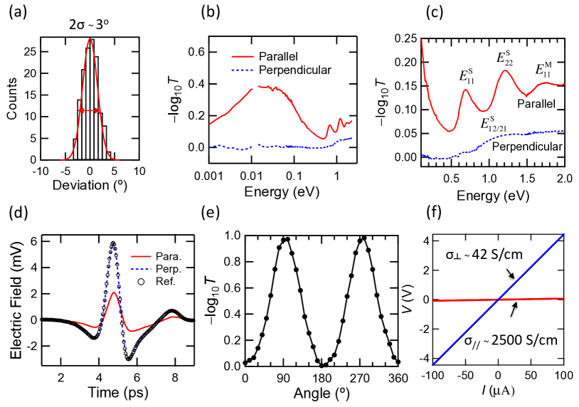
The parameter can be determined using polarization-dependent THz spectroscopy, through the equations in 3D and in 2D, where is the attenuation along the alignment direction and is the attenuation perpendicular to the alignment direction. These equations assume that the transition dipole is entirely parallel to the nanotube axis direction, which is valid for THz response of individual SWCNTs. Figure 6(d) shows time-domain waveforms of THz radiation transmitted through an aligned arc-discharge SWCNT film on an intrinsic silicon substrate for polarizations parallel and perpendicular to the alignment direction, together with a reference waveform obtained for the substrate alone. The data for the perpendicular case completely coincide with the reference trace; that is, no attenuation occurs within the SWCNT film. On the other hand, there is significant attenuation for the parallel case. Figure 6(e) shows a more detailed polarization-angle dependence of THz attenuation. The calculated is approximately 1, which is consistent with SEM analysis. Moreover, the obtained film shows strong anisotropic electronic conductivity (Figure 6(f)), with the conductivity along the alignment direction S/cm, the conductivity perpendicular to the alignment direction S/cm and the ratio between these two at room temperature.
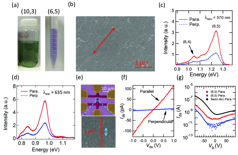
One of the most important features of controlled vacuum filtration is its universal applicability to any SWCNT suspensions, which allows us to capitalize on solution-based chirality separation techniques. Figure 7(a) demonstrates two images of separated semiconducting (10,3) and (6,5) mono-dispersed SWCNTs on a large scale, using gel chromatography and aqueous two phase extraction methods, respectively. Similarly, the fabricated chirality-enriched films show highly aligned and densely packed structures, as demonstrated in Figure 7(b). As semiconducting SWCNTs are optically pumped on resonance with the second interband transition (see Figure 1(e)), there is resonant emission at the energy of the first interband transition. Moreover, the SWCNTs are all aligned along the same direction, and thus the emitted light is linearly polarized, as shown in Figures 7(c)&(d).
The performance of electronic transistors made from semiconductor-enriched aligned films (Figure 7(e)) is better than that of their counterparts made from random films. As shown in Figures 7(f)&(g), the on-current density of the transistor in the parallel (perpendicular) direction is 2 nA m-1 (80 pA m-1), indicating that the on-current density can be improved by aligning the CNTs in one direction. The on-current density can be further enhanced by using larger diameter nanotubes, which is also demonstrated by our transistors based on semiconductor-enriched arc-discharge SWCNTs with an average diameter of 1.4 nm (Figure 7(g)). The device shows an enhancement of on-current density by 50 times compared to the (6,5) CNT transistor at the same drain-source voltage. All fabricated devices display decent on-off ratios , which can be improved by using a high- dielectric material or using a top-gate structure.
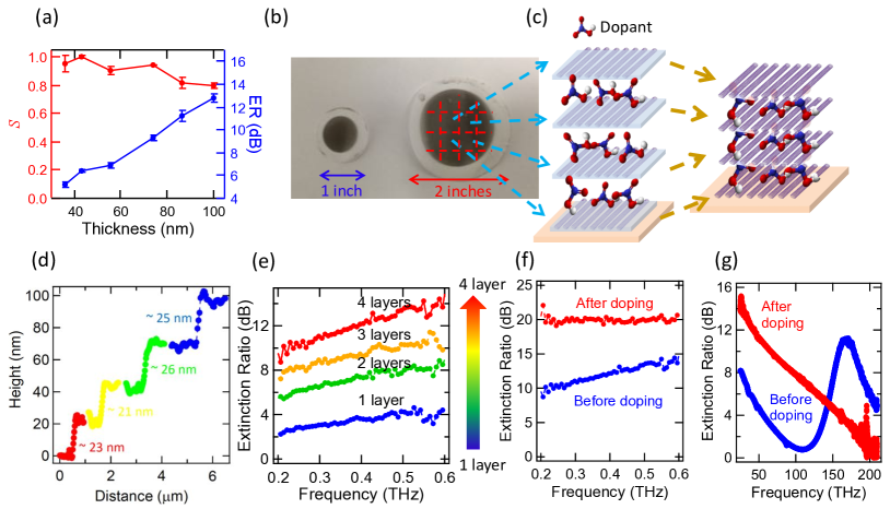
Obtained films can scale up both vertically and laterally and intercalate external molecules in between to form 3D architectures as shown by Komatsu et al. KomatsuEtAl2017AFM . By adjusting the filtrated volume during the controlled vacuum filtration process, the thicknesses of obtained films can be simply controlled, and they all display good alignment (Figure 8(a)). The extinction ratio (ER) of THz polarized attenuation can be as high as 120 dB/m, thanks to the high packing density in the films. On the other hand, the lateral size of obtained films is determined by the filtration system size. For instance, a 2-inch system can produce a larger film, compared to 1-inch systems. These 2-inch macroscopic crystalline SWCNT films enable us to build 3D architectures, through both layer stacking and molecule intercalation, as shown in Figure 8(c). This process consists of simple manual layer stacking with careful control of angles between layers and chemical doping by either electron donors or acceptors for -type or -type doping, respectively KomatsuEtAl2017AFM . These films are compatible with a wide spectrum of dopants, such as HNO3 GraupnerEtAl2003PCCP , H2SO4 GraupnerEtAl2003PCCP ; TantangEtAl2009C , NH4S2O8 TantangEtAl2009C , HCl GraupnerEtAl2003PCCP , H2SO3 SkakalovaEtAl2005JPC , iodine solution SkakalovaEtAl2005JPC , and benzyl vilogen HeEtAl2014NL . Figure 8(d) shows the height profile using AFM for four stacked layers, demonstrating this method as a consistent and well-controlled technique. The ER in the THz range increases as the film thickness and doping level increase, as shown in Figures 8(e)&(f). As the doping level (and thus Fermi level) is increased, the first interband transition is suppressed and eventually completely quenched; see Figure 8(g).
III Absorption of perpendicularly polarized light
Extremely confined 1D excitons with huge binding energies in semiconducting SWCNTs lead to a variety of optical properties AndoEtAl1997JPSJ ; KaneEtAl2003PRL ; ZhaoEtAl2004PRL ; WangEtAl2005S ; DukovicEtAl2005NL with light polarized along the SWCNT axis, while there are limited investigations of optical properties for light polarized perpendicular to the SWCNT axis, especially in a macroscopic SWCNT ensemble. The macroscopic crystalline films fabricated through controlled vacuum filtration provide a unique opportunity for such study. In this section, two examples – intersubband plasmons and crosspolarized excitons – are given.
Optical selection rules govern the observable transitions under far-field excitation. For light polarized parallel and perpendicular to the SWCNT axis, selection rules are different. Figure 9(a) schematically shows the band structure of metallic and semiconducting SWCNTs, respectively. Arrows of different colors show representative allowed optical transitions for light polarized along the tube axis (blue) and perpendicular to the tube axis (red and yellow). Conduction and valence subbands in metallic (semiconducting) nanotubes are indicated as C and V (C and V), respectively, where . Each subband has a well-defined angular momentum with quantum number and an eigenvalue of the Pauli matrix AndoEtAl2005JPSJ ; YanagiEtAl2018NC . Light with polarization parallel to the nanotube axis can cause transitions with . For light polarized perpendicular to the nanotube axis, the following selection rules have to be satisfied:
-
1.
, meaning that the angular momentum quantum number has to change by
-
2.
, meaning that the eigenvalue of the Pauli matrix has to be conserved.
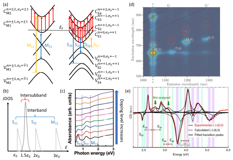
In undoped or lightly doped SWCNTs, optical absorption spectra are dominated by -conserving transitions (for example, the , , and transitions) for parallel polarization. Transitions for perpendicular polarization, such as the lowest-energy transitions and , are strongly suppressed due to the depolarization effect AjikiEtAl1994PCM ; UryuEtAl2006PRB . These transitions generate crosspolarized excitons. In heavily doped SWCNTs, where the Fermi level () is inside the conduction (valence) band, perpendicularly polarized light can excite the C C (V V) transition in metallic SWCNTs and the C C and C C (V V and V V) transitions in semiconducting SWCNTs. As has been shown in III-V semiconductor quantum wells, such as GaAs quantum wells LiuEtAl1999 , these intersubband transitions are intrinsically collective, deviating from the single-particle picture and involving many-body effects, and are thus termed intersubband plasmons (ISBPs). Unlike ISBPs in quantum wells with oblique incident light excitation, ISBPs in 1D SWCNTs can be excited under normal incidence. Also, different from crosspolarized excitons, ISBPs are expected to be strong due to the concentrated joint density-of-states (see Figure 9(b)) as well as the suppression of the depolarization effect at high SasakiEtAl2018PRA ; UryuEtAl2018PRB .
Previous studies of heavily doped SWCNTs have revealed a new peak KazaouiEtAl1999PRB ; KimEtAl2008JACS ; YanagiEtAl2011AM ; IgarashiEtAl2015PRL in absorption spectra. For example, as SWCNT films are heavily doped by AuCl3, a new peak emerges at 1.12 eV, as shown in Figure 9(c). However, in these cases, the nanotubes were randomly oriented, precluding definitive interpretation of the origin of this peak. On the other hand, crosspolarized excitons are significantly reduced, and it is challenging to observe this feature in single-CNT spectroscopy and studies of randomly oriented CNTs. For example, crosspolarized photoluminescence of a CNT suspension ChuangEtAl2008PRB (Figure 9(d)) and circular dichroism of (6,5) SWCNT enantiomer suspensions WeiEtAl2016NC (Figure 9(e)) have revealed these excitons, but any quantitative analysis such as oscillator strength estimation has not been possible. The crystalline SWCNT films produced by the controlled vacuum filtration technique are compatible with various dopants and electrolyte gating techniques and allow for a direct measurement using macroscopic spectroscopy techniques. These samples enable us unambiguous determination of these optical features occurring when light is polarized perpendicular to the nanotube axis.
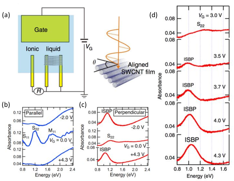
First, we discuss recently reported direct evidence for ISBPs in gated and aligned SWCNTs through polarization-dependent absorption spectroscopy by Yanagi et al., which elucidates the origin of the observed unknown feature in these previous studies on doped SWCNTs YanagiEtAl2018NC . A film of macroscopically aligned and packed SWCNTs with an average diameter of 1.4 nm, containing both metallic and semiconducting SWCNTs, was prepared using controlled vacuum filtration. The was tuned using electrolyte gating techniques YanagiEtAl2011AM ; IgarashiEtAl2015PRL . A schematic illustration of the experimental setup is shown in Figure 10(a). Figure 10(b) shows parallel-polarization optical absorption spectra for the film at three gate voltages, 2.0, 0.0 and 4.3 V. At 0.0 V, the interband transitions and in semiconducting nanotubes and the interband transition in metallic nanotubes are clearly observed. As the gate voltage is increased in the positive (negative) direction, electrons (holes) are injected into the nanotubes through formation of an electric double layer on their surfaces. As a result, the , , and peaks disappear at 2.0 and 4.3 V because of Pauli blocking.
Completely different behavior is observed in perpendicular-polarization spectra, as shown in Figure 10(c). As is increased, a new absorption peak due to ISBP appears at 1 eV, grows in intensity, and dominates the spectrum at the highest . The properties of the ISBP peak are entirely orthogonal to those of the , , and peaks. Figure 10(d) shows detailed changes of the ISBP peak for this aligned film as the gate voltage is varied on the electron injection side. The peak first appears at 1 eV when the gate voltage reaches 3 V, and then its intensity gradually increases with increasing . In addition, the peak position blue shifts with further increasing , reaching 1.05 eV at 4.3 V.
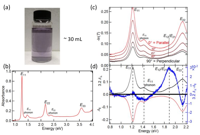
Second, a systematic polarization-dependent optical absorption spectroscopy study of a macroscopic film of highly aligned single-chirality (6,5) SWCNTs was performed for the observation of crosspolarized excitons KatsutaniEtAl2018APA . Recent advances in pH-controlled gel chromatography YomogidaEtAl2016NC ; IchinoseEtAl2017JPC enables the preparation of a large-scale suspension of chirality-enriched semiconducting SWCNTs with extremely high purity. Figure 11(a) shows an example of 30 mL suspension of (6,5) SWCNTs. This industry-scale separation YomogidaEtAl2016NC is highly desirable for the vacuum filtration technique to produce aligned films. Figure 11(b) demonstrates an absorption spectrum for the obtained suspension, where only transitions associated with (6,5) SWCNTs are observed, such as , , , and their phonon sidebands. The chirality purity is estimated to be KatsutaniEtAl2018APA ; IchinoseEtAl2017JPC . As the polarization of the incident light rotates, the attenuation of the transmitted light changes accordingly. Figure 11(c) displays representative spectra at angles of 0∘, 30∘, 60∘ and 90∘. Absorption peaks associated with allowed transitions for parallel polarization () are strongly anisotropic. Although there is still prominent absorption at 90∘ due to imperfect alignment, there is a clearly observable new feature at 1.9 eV in the perpendicular polarization case () from the crosspolarized excitons /. Figure 11(d) shows the / feature in a more clear manner. The baseline was subtracted, and then a spectrum, showing multiplied by 3.2 and subtracted by , is presented. Further detailed analysis based on nematic order parameters revealed that the oscillator strength for () is 1/10 of the oscillator strength of () KatsutaniEtAl2018APA .
IV Microcavity exciton-polaritons in aligned semiconducting SWCNTs
Strong coupling of photons and excitons inside a microcavity produces hybrid quasiparticles, microcavity exciton-polaritons, which continue to stimulate much interest KhitrovaEtAl1999RMP ; DengEtAl2010RMP ; GibbsEtAl2011NP . In a general model, a two-level system interacts with photons inside a microcavity, with the coupling strength and photon (matter) decay rate (). Resonant coupling leads to a splitting into two normal modes with an energy separation, , known as the vacuum Rabi splitting (VRS), with 2 when . Depending on the relationship between and , , there are different regimes Forn-DiazEtAl2018APA . The strong coupling regime is achieved when 4 1. Furthermore, the ultrastrong coupling regime arises when 0.1, where is the resonance energy, whereas the deep strong coupling regime is defined as 1 CasanovaEtAl2010PRL .
Microcavity exciton-polaritons based on semiconductor quantum wells have been a model system for highlighting the difference between light-atom-coupling and light-condensed-matter-coupling. However, they remain in the strong coupling regime typically with 10-2. Furthermore, the fabrication of such devices usually requires sophisticated molecular beam epitaxy, and measurements have to be done at cryogenic temperatures. Excitons in organic semiconductors, possessing large binding energies and oscillator strengths, have displayed larger VRS LidzeyetAl98Nature ; GambinoEtAl2014P at room temperature. Moreover, nanomaterials, such as transition metal dichalcogenides LiuEtAl2015NP and semiconducting SWCNTs GrafEtAl2016Nc ; GrafEtAl2017NM , have recently emerged as a new platform for studying strong-coupling physics under extreme quantum confinement. Large oscillator strengths in these materials help relax the stringent requirement for a high quality factor (high-) photonic cavity. In particular for SWCNTs, Graf et al. first reported near-infrared microcavity exciton-polaritons by incorporating a film of polymer-selected chirality-enriched (6,5) SWCNTs of random orientation inside a Fabry-Pérot microcavity, simply consisting of two parallel metal mirrors GrafEtAl2016Nc . Cavities of similar structures are widely used in organic molecule exciton-polaritons. A very large VRS, exceeding 100 meV, was observed to scale proportionally to , where is the number of SWCNTs inside the cavity, displaying a cooperative enhancement GrafEtAl2016Nc . Furthermore, electrical pumping of exciton-polaritons was achieved by the same group GrafEtAl2017NM , paving the way toward carbon-based polariton emitters and lasers.
More recently, Gao and coworkers developed a unique architecture in which excitons in an aligned single-chirality (6,5) CNT film interact with cavity photons in a polarization-dependent manner GaoEtAl2018NP . Again, they prepared aligned (6,5) films by vacuum filtrating suspensions separated using the aqueous two phase extraction method. The microcavity exciton-polariton devices were created by embedding the obtained aligned film with thickness inside a Fabry-Pérot cavity. By changing the incidence angle ( in Figure 12(a)), the resonance frequency of the microcavity was tuned to resonate with the or of (6,5) SWCNTs. Furthermore, adjustment of the angle between the incident light polarization direction and the SWCNT alignment direction ( in Figure 12(a)) provided a convenient knob to probe the directional variation of . The angle has a one-to-one correspondence with the in-plane wave vector , so the dependence of transmission peaks can be converted into or dependence for 0∘ or 90∘, respectively, to map out polariton dispersions. Figures 12(b)&(c) show experimental and simulated in-plane dispersion relationships for a device with 8 nm for 0∘ and 90∘, respectively. A prominent VRS of 137 6 meV ( 5.5%) is observed, while no splitting is seen at 90∘. Here, is the resonance frequency of . Furthermore, any value of VRS between zero and its maximum value can be selected, on demand, by setting the polarization angle (Figure 12(d)).
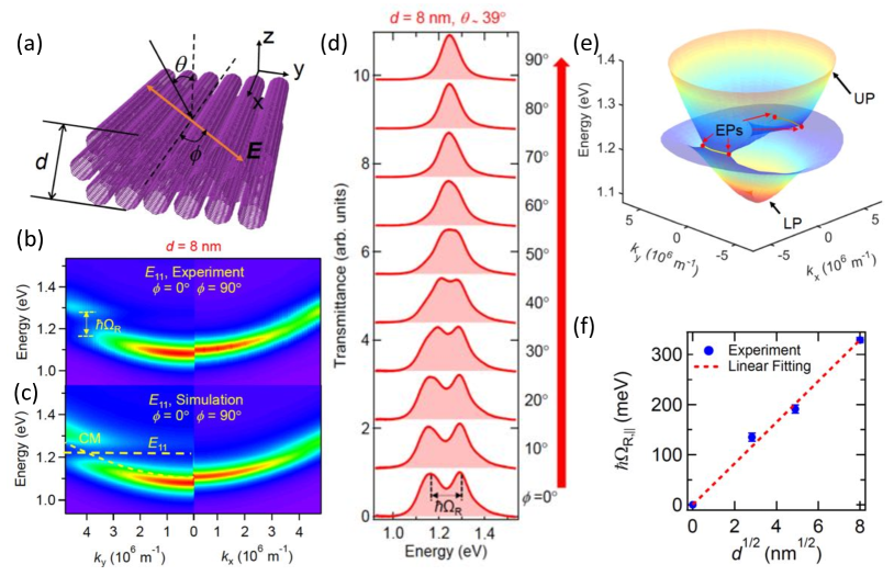
Since the in-plane wavevector () has one-to-one correspondence with (), the continuous adjustment of and maps out the full anisotropic SWCNT exciton polariton dispersion surfaces, as demonstrated in Figure 12(e) for the 8-nm-thick device. The most striking feature of Figure 12(e) is the appearance of two circular arcs on which the energy is constant; namely, the upper polariton (UP) and lower polariton (LP) branches coalesce to form these constant-energy arcs in momentum space. Furthermore, Gao et al. analyzed the obtained spectra using quantum Langevin equations, including losses, and demonstrated that the end points of each arc are exceptional points, that is, spectral singularities that ubiquitously appear in open or dissipative systems. Finally, Figure 12(f) confirms that VRS scales with and thus . The VRS value for the 64-nm-thick device was 329 meV ( 13.3%), which is the largest value ever reported for exciton polaritons based on Wannier excitons.
V Plasmon resonances and hybridization in patterned aligned SWCNTs
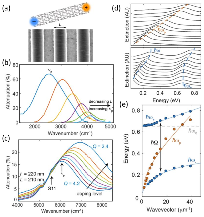
The longitudinal confinement of free carriers in finite-length SWCNTs leads to a prominent broad absorption peak in the THz and infrared ranges ZhangEtAl2013NL ; HeEtAl2016NN , as shown in Figure 6(b). Temperature-dependent broadband spectroscopy unambiguously revealed the plasmonic nature in films of randomly oriented SWCNTs ZhangEtAl2013NL . Resonance energy depends on the length of SWCNT and can be tuned by adjusting the nanotube length through sonication processes of different duration MorimotoEtAl2014N . However, due to a broad length distribution in these films, the linewidth of the resonance is usually broad and the resonance peak position is up to cm-1 in the far-infrared. Crystalline SWCNT films produced using the controlled vacuum filtration method, which are compatible with various micro/nanofabrication techniques such as lithography and etching, provide a unique platform for unifying CNT lengths for high quality plasmon resonators. The longitudinal confinement, determined by the lithography-defined dimensions, can range from tens to hundreds of nanometers. In combination with chemical doping techniques, the resonance frequency can be broadly tuned from the THz to near-infrared.
Figure 13(a) illustrates the bounded electron oscillation in SWCNTs and a representative SEM image of patterned strips of aligned films of SWCNTs produced through controlled vacuum filtration reported by Chiu et al. ChiuEtAl2017NL . For strips of a 165-nm-thick film, there are strong attenuation peaks () in the midinfrared range. As the lateral dimension () decreases from 800 nm to 100 nm at fixed film thickness (), blue-shifts and increases up to 9; see Figure 13(b). This increase of the factor reflects the increased length uniformity in smaller- devices. Furthermore, exposure to strong dopants, such as HNO3, increases the film conductivity and pushes further to the near-infrared, as shown in Figure 13(c). The presence of dopants, however, reduces the factor from 4.2 to 2.4, because of an increase of scattering.
As dopants are introduced and the is elevated, the lowest-energy excitons in semiconducting SWCNTs, , in these films are switched off; see Figure 8(g) and Figure 9(a). There is a single resonance peak as is tuned, as shown in the top panel of Figure 13(e). After films are annealed to remove excess dopants, exciton transitions are activated with the transition energy at eV. As is continuously adjusted and thus is continuously tuned across , strong coupling between plasmon and exciton resonances emerges; see the bottom panel of Figure 13(d). The formed new quasiparticles are known as plexcitons. Figure 13(e) demonstrates the peak energies for the LP branch, UP branch, and bare plasmon resonances in highly doped films. An extremely large VRS meV () is observed, indicating ultrastrong coupling. A Hopfield-like Hamiltonian can fully capture the polariton dispersions HoEtAl2018APA . Moreover, the coupling strength can be tuned by adjusting the doping level and film thickness. The increase of doping level, thus film conductivity, decreases the oscillator strength of and the coupling strength.
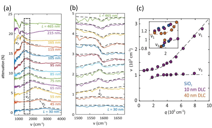
In addition to plexcitons, these plasmon resonances in strips of aligned SWCNTs can strongly couple with other quasiparticles, such as phonons. Falk et al. showed strong coupling between longitudinal optical phonons in SiO2 substrates (attenuation peak in Figure 14(a)), infrared-active and phonons in CNTs KuhlmannEtAl1998CPL ; LapointeEtAl2012PRL (attenuation peak in Figure 14(a)) and plasmon resonances (attenuation peak in Figure 14(a)), by putting patterned strips with various of aligned SWCNT films on SiO2 substrates. The strong coupling enhances usually weak infrared-active phonons and leads to an asymmetric lineshape, which can be fit very well with a Fano resonance formula FalkEtAl2017PRL , as shown in Figure 14(b). Peak positions of and demonstrate a clear anticrossing behavior, as displayed in Figure 14(c).
VI Conclusion
This review summarizes the recent achievement of fabricating wafer-scale crystalline CNTs and the discovery of new science and applications in these new materials, specifically in photonics and optoelectronics. These wafer-scale crystalline CNTs with control of chirality distribution fabricated through controlled vacuum filtration open new pathways toward both fundamental studies and various applications in a diverse set of disciplines. This technique addresses the grand ”bottom-to-top” challenge in the CNT community for utilizing extraordinary properties of individual CNTs at the nanoscale to macroscopic applications. We anticipate that the initial studies described in this review will further stimulate interest in CNT research and push toward real-world applications employing CNTs.
Funding. This work was supported by the Department of Energy Basic Energy Sciences through Grant No. DE-FG02-06ER46308, the National Science Foundation through Award No. ECCS-1708315, and the Robert A. Welch Foundation through Grant No. C-1509.
Acknowledgments. We thank G. Timothy Noe for his help with editing and proofreading a draft version of this article. Some of the work presented in this article was originally carried out in collaboration with Xiaowei He, Fumiya Katsutani, Xinwei Li, and Natsumi Komatsu from Rice University, and Kazuhiro Yanagi from Tokyo Metropolitan University.
References
- (1) Jorio A, Dresselhaus G, Dresselhaus MS, editors. 2008 Carbon Nanotubes: Advanced Topics in the Synthesis, Structure, Properties and Applications. Springer Berlin Heidelberg 1 edition.
- (2) Hirsch A. 2010 The era of carbon allotropes. Nat. Mater. 9, 868.
- (3) Kroto HW, Heath JR, O’Brien SC, Curl RF, Smalley RE. 1985 C60: Buckminsterfullerene. Nature 318, 162.
- (4) Iijima S. 1991 Helical microtubules of graphitic carbon. Nature 354, 56.
- (5) Novoselov KS, Geim AK, Morozov SV, Jiang D, Zhang Y, Dubonos SV, Grigorieva IV, Firsov AA. 2004 Electric field effect in atomically thin carbon films. Science 306, 666–669.
- (6) Geim A, Novoselov K et al.. 2007 The rise of graphene. Nat. Mater. 6, 183–191.
- (7) Avouris P, Freitag M, Perebeinos V. 2008 Carbon-nanotube photonics and optoelectronics. Nat. Photonics 2, 341.
- (8) Nanot S, Hároz EH, Kim JH, Hauge RH, Kono J. 2012 Optoelectronic Properties of Single-Wall Carbon Nanotubes. Adv. Mater. 24, 4977–4994.
- (9) Nanot S, Thompson NA, Kim JH, Wang X, Rice WD, Hároz EH, Ganesan Y, Pint CL, Kono J. 2013 Single-Walled Carbon Nanotubes. In Vajtai R, editor, Handbook of Nanomaterials , pp. 105–146. Springer, Berlin.
- (10) Ando T, Nakanishi T. 1998 Impurity scattering in carbon nanotubes–absence of back scattering–. J. Phys. Soc. Jpn. 67, 1704–1713.
- (11) Tans SJ, Devoret MH, Dai H, Thess A, Smalley RE, Geerligs L, Dekker C. 1997 Individual single-wall carbon nanotubes as quantum wires. Nature 386, 474.
- (12) Dürkop T, Getty S, Cobas E, Fuhrer M. 2004 Extraordinary mobility in semiconducting carbon nanotubes. Nano Lett. 4, 35–39.
- (13) Park S, Vosguerichian M, Bao Z. 2013 A review of fabrication and applications of carbon nanotube film-based flexible electronics. Nanoscale 5, 1727–1752.
- (14) Murakami Y, Chiashi S, Miyauchi Y, Hu M, Ogura M, Okubo T, Maruyama S. 2004 Growth of vertically aligned single-walled carbon nanotube films on quartz substrates and their optical anisotropy. Chem. Phys. Lett. 385, 298–303.
- (15) Kocabas C, Hur SH, Gaur A, Meitl MA, Shim M, Rogers JA. 2005 Guided growth of large-scale, horizontally aligned arrays of single-walled carbon nanotubes and their use in thin-film transistors. Small 1, 1110–1116.
- (16) Meitl MA, Zhou Y, Gaur A, Jeon S, Usrey ML, Strano MS, Rogers JA. 2004 Solution casting and transfer printing single-walled carbon nanotube films. Nano Lett. 4, 1643–1647.
- (17) Begtrup G, Ray KG, Kessler BM, Yuzvinsky TD, Garcia H, Zettl A. 2007 Extreme thermal stability of carbon nanotubes. physica status solidi (b) 244, 3960–3963.
- (18) Mori T, Yamauchi Y, Honda S, Maki H. 2014 An electrically driven, ultrahigh-speed, on-chip light emitter based on carbon nanotubes. Nano Lett. 14, 3277–3283.
- (19) Kang SJ, Kocabas C, Ozel T, Shim M, Pimparkar N, Alam MA, Rotkin SV, Rogers JA. 2007 High-performance electronics using dense, perfectly aligned arrays of single-walled carbon nanotubes. Nat. Nanotechnol. 2, 230.
- (20) Avery AD, Zhou BH, Lee J, Lee ES, Miller EM, Ihly R, Wesenberg D, Mistry KS, Guillot SL, Zink BL et al.. 2016 Tailored semiconducting carbon nanotube networks with enhanced thermoelectric properties. Nat. Energy. 1, 16033.
- (21) Cao Q, Kim Hs, Pimparkar N, Kulkarni JP, Wang C, Shim M, Roy K, Alam MA, Rogers JA. 2008 Medium-scale carbon nanotube thin-film integrated circuits on flexible plastic substrates. Nature 454, 495.
- (22) He X, Wang X, Nanot S, Cong K, Jiang Q, Kane AA, Goldsmith JE, Hauge RH, Léonard F, Kono J. 2013 Photothermoelectric p–n junction photodetector with intrinsic broadband polarimetry based on macroscopic carbon nanotube films. ACS Nano 7, 7271–7277.
- (23) He X, Léonard F, Kono J. 2015 Uncooled carbon nanotube photodetectors. Adv. Opt. Mater. 3, 989–1011.
- (24) Jung Y, Li X, Rajan NK, Taylor AD, Reed MA. 2012 Record high efficiency single-walled carbon nanotube/silicon p–n junction solar cells. Nano Lett. 13, 95–99.
- (25) Wu Z, Chen Z, Du X, Logan JM, Sippel J, Nikolou M, Kamaras K, Reynolds JR, Tanner DB, Hebard AF et al.. 2004 Transparent, conductive carbon nanotube films. Science 305, 1273–1276.
- (26) Rouhi N, Jain D, Burke PJ. 2011 High-performance semiconducting nanotube inks: Progress and prospects. ACS Nano 5, 8471–8487.
- (27) Sarker BK, Shekhar S, Khondaker SI. 2011 Semiconducting enriched carbon nanotube aligned arrays of tunable density and their electrical transport properties. ACS Nano 5, 6297–6305.
- (28) Murakami Y, Miyauchi Y, Chiashi S, Maruyama S. 2003 Direct synthesis of high-quality single-walled carbon nanotubes on silicon and quartz substrates. Chem. Phys. Lett. 377, 49–54.
- (29) Hata K, Futaba DN, Mizuno K, Namai T, Yumura M, Iijima S. 2004 Water-assisted highly efficient synthesis of impurity-free single-walled carbon nanotubes. Science 306, 1362–1364.
- (30) Pint CL, Pheasant ST, Parra-Vasquez ANG, Horton C, Xu Y, Hauge RH. 2009 Investigation of optimal parameters for oxide-assisted growth of vertically aligned single-walled carbon nanotubes. J. Phys. Chem. C 113, 4125–4133.
- (31) Joselevich E, Dai H, Liu J, Hata K, Windle AH. 2007 Carbon nanotube synthesis and organization. In Carbon nanotubes , pp. 101–165. Springer.
- (32) Pint CL, Xu YQ, Moghazy S, Cherukuri T, Alvarez NT, Haroz EH, Mahzooni S, Doorn SK, Kono J, Pasquali M et al.. 2010 Dry contact transfer printing of aligned carbon nanotube patterns and characterization of their optical properties for diameter distribution and alignment. ACS nano 4, 1131–1145.
- (33) Zhang Y, Chang A, Cao J, Wang Q, Kim W, Li Y, Morris N, Yenilmez E, Kong J, Dai H. 2001 Electric-field-directed growth of aligned single-walled carbon nanotubes. Appl. Phys. Lett. 79, 3155–3157.
- (34) Huang S, Cai X, Du C, Liu J. 2003 Oriented long single walled carbon nanotubes on substrates from floating catalysts. J. Phys. Chem. B 107, 13251–13254.
- (35) Yang F, Wang X, Zhang D, Yang J, Luo D, Xu Z, Wei J, Wang JQ, Xu Z, Peng F et al.. 2014 Chirality-specific growth of single-walled carbon nanotubes on solid alloy catalysts. Nature 510, 522.
- (36) Sanchez-Valencia JR, Dienel T, Gröning O, Shorubalko I, Mueller A, Jansen M, Amsharov K, Ruffieux P, Fasel R. 2014 Controlled synthesis of single-chirality carbon nanotubes. Nature 512, 61.
- (37) Zhang S, Kang L, Wang X, Tong L, Yang L, Wang Z, Qi K, Deng S, Li Q, Bai X et al.. 2017 Arrays of horizontal carbon nanotubes of controlled chirality grown using designed catalysts. Nature 543, 234.
- (38) Ding L, Yuan D, Liu J. 2008 Growth of high-density parallel arrays of long single-walled carbon nanotubes on quartz substrates. J. Am. Chem. Soc. 130, 5428–5429.
- (39) Druzhinina T, Hoeppener S, Schubert US. 2011 Strategies for post-synthesis alignment and immobilization of carbon nanotubes. Adv. Mater. 23, 953–970.
- (40) Zheng M, Jagota A, Strano MS, Santos AP, Barone P, Chou SG, Diner BA, Dresselhaus MS, Mclean RS, Onoa GB et al.. 2003 Structure-based carbon nanotube sorting by sequence-dependent DNA assembly. Science 302, 1545–1548.
- (41) Tu X, Manohar S, Jagota A, Zheng M. 2009 DNA sequence motifs for structure-specific recognition and separation of carbon nanotubes. Nature 460, 250.
- (42) Nish A, Hwang JY, Doig J, Nicholas RJ. 2007 Highly selective dispersion of single-walled carbon nanotubes using aromatic polymers. Nat. Nanotechnol. 2, 640.
- (43) Arnold MS, Green AA, Hulvat JF, Stupp SI, Hersam MC. 2006 Sorting carbon nanotubes by electronic structure using density differentiation. Nat. Nanotechnol. 1, 60.
- (44) Ghosh S, Bachilo SM, Weisman RB. 2010 Advanced sorting of single-walled carbon nanotubes by nonlinear density-gradient ultracentrifugation. Nat. Nanotechnol. 5, 443.
- (45) Liu H, Nishide D, Tanaka T, Kataura H. 2011 Large-scale single-chirality separation of single-wall carbon nanotubes by simple gel chromatography. Nat. Commun. 2, 309.
- (46) Khripin CY, Fagan JA, Zheng M. 2013 Spontaneous partition of carbon nanotubes in polymer-modified aqueous phases. J. Am. Chem. Soc. 135, 6822–6825.
- (47) Fagan JA, Khripin CY, Silvera Batista CA, Simpson JR, Hároz EH, Hight Walker AR, Zheng M. 2014 Isolation of specific small-diameter single-wall carbon nanotube species via aqueous two-phase extraction. Adv. Mater. 26, 2800–2804.
- (48) Zhang M, Atkinson KR, Baughman RH. 2004 Multifunctional carbon nanotube yarns by downsizing an ancient technology. Science 306, 1358–1361.
- (49) Smith B, Benes Z, Luzzi D, Fischer J, Walters D, Casavant M, Schmidt J, Smalley R. 2000 Structural anisotropy of magnetically aligned single wall carbon nanotube films. Appl. Phys. Lett. 77, 663–665.
- (50) Shekhar S, Stokes P, Khondaker SI. 2011 Ultrahigh density alignment of carbon nanotube arrays by dielectrophoresis. ACS Nano 5, 1739–1746.
- (51) Engel M, Small JP, Steiner M, Freitag M, Green AA, Hersam MC, Avouris P. 2008 Thin film nanotube transistors based on self-assembled, aligned, semiconducting carbon nanotube arrays. ACS Nano 2, 2445–2452.
- (52) Shastry TA, Seo JWT, Lopez JJ, Arnold HN, Kelter JZ, Sangwan VK, Lauhon LJ, Marks TJ, Hersam MC. 2013 Large-Area, Electronically Monodisperse, Aligned Single-Walled Carbon Nanotube Thin Films Fabricated by Evaporation-Driven Self-Assembly. Small 9, 45–51.
- (53) Li X, Zhang L, Wang X, Shimoyama I, Sun X, Seo WS, Dai H. 2007 Langmuir- Blodgett assembly of densely aligned single-walled carbon nanotubes from bulk materials. J. Am. Chem. Soc. 129, 4890–4891.
- (54) Cao Q, Han Sj, Tulevski GS, Zhu Y, Lu DD, Haensch W. 2013 Arrays of single-walled carbon nanotubes with full surface coverage for high-performance electronics. Nat. Nanotechnol. 8, 180.
- (55) Dierking I, Scalia G, Morales P. 2005 Liquid crystal–carbon nanotube dispersions. J. Appl. Phys. 97, 044309.
- (56) Lagerwall JP, Scalia G. 2008 Carbon nanotubes in liquid crystals. J. Mater. Chem. 18, 2890–2898.
- (57) Badaire S, Zakri C, Maugey M, Derré A, Barisci JN, Wallace G, Poulin P. 2005 Liquid crystals of DNA-stabilized carbon nanotubes. Adv. Mater. 17, 1673–1676.
- (58) Mclean RS, Huang X, Khripin C, Jagota A, Zheng M. 2006 Controlled two-dimensional pattern of spontaneously aligned carbon nanotubes. Nano Lett. 6, 55–60.
- (59) Dan B, Ma AW, Hároz EH, Kono J, Pasquali M. 2012 Nematic-like alignment in SWNT thin films from aqueous colloidal suspensions. Ind. Eng. Chem. Res. 51, 10232–10237.
- (60) He X, Gao W, Xie L, Li B, Zhang Q, Lei S, Robinson JM, Hároz EH, Doorn SK, Wang W, Vajtai R, Ajayan PM, Adams WW, Hauge RH, Kono J. 2016 Wafer-Scale Monodomain Films of Spontaneously Aligned Single-Walled Carbon Nanotubes. Nat. Nanotechnol. 11, 633–638.
- (61) Ma PC, Siddiqui NA, Marom G, Kim JK. 2010 Dispersion and functionalization of carbon nanotubes for polymer-based nanocomposites: a review. Composites Part A: Applied Science and Manufacturing 41, 1345–1367.
- (62) Hároz EH, Duque JG, Lu BY, Nikolaev P, Arepalli S, Hauge RH, Doorn SK, Kono J. 2012 Unique origin of colors of armchair carbon nanotubes. J. Am. Chem. Soc. 134, 4461–4464
- (63) Green AA, Hersam MC. 2008 Colored semitransparent conductive coatings consisting of monodisperse metallic single-walled carbon nanotubes. Nano Lett. 8, 1417–1422.
- (64) Ho PH, Farmer DB, Tulevski GS, Han SJ, Bishop DM, Gignac LM, Bucchignano J, Avouris P, Falk AL. 2018 Intrinsically ultrastrong light-matter interactions in crystalline films of carbon nanotubes. arXiv:1803.01087.
- (65) Chiu KC, Falk AL, Ho PH, Farmer DB, Tulevski G, Lee YH, Avouris P, Han SJ. 2017 Strong and broadly tunable plasmon resonances in thick films of aligned carbon nanotubes. Nano Lett. 17, 5641–5645.
- (66) Zhang Q, Hároz EH, Jin Z, Ren L, Wang X, Arvidson RS, Lüttge A, Kono J. 2013 Plasmonic nature of the terahertz conductivity peak in single-wall carbon nanotubes. Nano Lett 13, 5991–5996.
- (67) Ajiki H, Ando T. 1994 Aharonov-Bohm effect in carbon nanotubes. Physica B 201, 349–352.
- (68) Ando T. 2005 Theory of electronic states and transport in carbon nanotubes. J. Phys. Soc. Jpn. 74, 777–817.
- (69) Uryu S, Ando T. 2006 Exciton absorption of perpendicularly polarized light in carbon nanotubes. Phys. Rev. B 74, 155411.
- (70) Komatsu N, Gao W, Chen P, Guo C, Babakhani A, Kono J. 2017 Modulation-Doped Multiple Quantum Wells of Aligned Single-Wall Carbon Nanotubes. Adv. Funct. Mater. 27, 1606022.
- (71) Graupner R, Abraham J, Vencelová A, Seyller T, Hennrich F, Kappes MM, Hirsch A, Ley L. 2003 Doping of single-walled carbon nanotube bundles by Brønsted acids. Phys. Chem. Chem. Phys. 5, 5472–5476.
- (72) Tantang H, Ong JY, Loh CL, Dong X, Chen P, Chen Y, Hu X, Tan LP, Li LJ. 2009 Using oxidation to increase the electrical conductivity of carbon nanotube electrodes. Carbon 47, 1867–1870.
- (73) Skakalova V, Kaiser A, Dettlaff-Weglikowska U, Hrncarikova K, Roth S. 2005 Effect of chemical treatment on electrical conductivity, infrared absorption, and Raman spectra of single-walled carbon nanotubes. J. Phys. Chem. B 109, 7174–7181.
- (74) He X, Fujimura N, Lloyd JM, Erickson KJ, Talin AA, Zhang Q, Gao W, Jiang Q, Kawano Y, Hauge RH et al.. 2014 Carbon nanotube terahertz detector. Nano Lett. 14, 3953–3958.
- (75) Ando T. 1997 Excitons in carbon nanotubes. J. Phys. Soc. Jpn. 66, 1066–1073.
- (76) Kane C, Mele E. 2003 Ratio problem in single carbon nanotube fluorescence spectroscopy. Phys. Rev. Lett. 90, 207401.
- (77) Zhao H, Mazumdar S. 2004 Electron-electron interaction effects on the optical excitations of semiconducting single-walled carbon nanotubes. Phys. Rev. Lett. 93, 157402.
- (78) Wang F, Dukovic G, Brus LE, Heinz TF. 2005 The optical resonances in carbon nanotubes arise from excitons. Science 308, 838–841.
- (79) Dukovic G, Wang F, Song D, Sfeir MY, Heinz TF, Brus LE. 2005 Structural dependence of excitonic optical transitions and band-gap energies in carbon nanotubes. Nano Lett. 5, 2314–2318.
- (80) Yanagi K, Okada R, Ichinose Y, Yomogida Y, Katsutani F, Gao W, Kono J. 2018 Intersubband plasmons in the quantum limit in gated and aligned carbon nanotubes. Nat. Commun. 9, 1121.
- (81) Kim KK, Bae JJ, Park HK, Kim SM, Geng HZ, Park KA, Shin HJ, Yoon SM, Benayad A, Choi JY et al.. 2008 Fermi level engineering of single-walled carbon nanotubes by AuCl3 doping. J. Am. Chem. Soc. 130, 12757–12761.
- (82) Chuang KC, Nish A, Hwang JY, Evans G, Nicholas R et al.. 2008 Experimental study of Coulomb corrections and single-particle energies for single-walled carbon nanotubes using cross-polarized photoluminescence. Phys. Rev. B 78, 085411.
- (83) Wei X, Tanaka T, Yomogida Y, Sato N, Saito R, Kataura H. 2016 Experimental determination of excitonic band structures of single-walled carbon nanotubes using circular dichroism spectra. Nat. Commun. 7, 12899.
- (84) Liu H, Capasso F. 1999 Intersubband transitions in quantum wells: Physics and device applications vol. 5. Academic Press.
- (85) Sasaki K, Tokura Y. 2018 Theory of a Carbon-Nanotube Polarization Switch. Phys. Rev. Applied 9, 034018.
- (86) Uryu S. 2018 Numerical study of cross-polarized plasmons in doped carbon nanotubes. Phys. Rev. B 97, 125420.
- (87) Kazaoui S, Minami N, Jacquemin R, Kataura H, Achiba Y. 1999 Amphoteric doping of single-wall carbon-nanotube thin films as probed by optical absorption spectroscopy. Phys. Rev. B 60, 13339.
- (88) Yanagi K, Moriya R, Yomogida Y, Takenobu T, Naitoh Y, Ishida T, Kataura H, Matsuda K, Maniwa Y. 2011 Electrochromic Carbon Electrodes: Controllable Visible Color Changes in Metallic Single-Wall Carbon Nanotubes. Adv. Mater. 23, 2811–2814.
- (89) Igarashi T, Kawai H, Yanagi K, Cuong NT, Okada S, Pichler T. 2015 Tuning localized transverse surface plasmon resonance in electricity-selected single-wall carbon nanotubes by electrochemical doping. Phys. Rev. Lett. 114, 176807.
- (90) Katsutani F, Gao W, Li X, Ichinose Y, Yomogida Y, Yanagi K, Kono J. 2018 Direct Observation of Cross-Polarized Excitons in Aligned Single-Chirality Single-Wall Carbon Nanotubes. arXiv:1808.08602.
- (91) Yomogida Y, Tanaka T, Zhang M, Yudasaka M, Wei X, Kataura H. 2016 Industrial-scale separation of high-purity single-chirality single-wall carbon nanotubes for biological imaging. Nat. Commun. 7, 12056.
- (92) Ichinose Y, Eda J, Yomogida Y, Liu Z, Yanagi K. 2017 Extraction of high-purity single-chirality single-walled carbon nanotubes through precise pH control using carbon dioxide bubbling. J. Phys. Chem. C 121, 13391–13395.
- (93) Khitrova G, Gibbs H, Jahnke F, Kira M, Koch S. 1999 Nonlinear optics of normal-mode-coupling semiconductor microcavities. Rev. Mod. Phys. 71, 1591.
- (94) Deng H, Haug H, Yamamoto Y. 2010 Exciton-polariton bose-einstein condensation. Rev. Mod. Phys. 82, 1489.
- (95) Gibbs H, Khitrova G, Koch S. 2011 Exciton–polariton light–semiconductor coupling effects. Nat. Photonics 5, 273.
- (96) Forn-Díaz P, Lamata L, Rico E, Kono J, Solano E. 2018 Ultrastrong coupling regimes of light-matter interaction. arXiv:1804.09275.
- (97) Casanova J, Romero G, Lizuain I, García-Ripoll JJ, Solano E. 2010 Deep Strong Coupling Regime of the Jaynes-Cummings Model. Phys. Rev. Lett. 105, 263603.
- (98) Lidzey DG, Bradley D, Skolnick M, Virgili T, Walker S, Whittaker D. 1998 Strong Exciton–Photon Coupling in an Organic Semiconductor Microcavity. Nature 395, 53–55.
- (99) Gambino S, Mazzeo M, Genco A, Di Stefano O, Savasta S, Patanè S, Ballarini D, Mangione F, Lerario G, Sanvitto D et al.. 2014 Exploring Light–Matter Interaction Phenomena under Ultrastrong Coupling Regime. ACS Photonics 1, 1042–1048.
- (100) Liu X, Galfsky T, Sun Z, Xia F, Lin Ec, Lee YH, Kéna-Cohen S, Menon VM. 2015 Strong light–matter coupling in two-dimensional atomic crystals. Nat. Photonics 9, 30–34.
- (101) Graf A, Tropf L, Zakharko Y, Zaumseil J, Gather MC. 2016 Near-infrared exciton-polaritons in strongly coupled single-walled carbon nanotube microcavities. Nat. Commun. 7, 13078.
- (102) Graf A, Held M, Zakharko Y, Tropf L, Gather MC, Zaumseil J. 2017 Electrical pumping and tuning of exciton-polaritons in carbon nanotube microcavities. Nat. Mater. 16, 911.
- (103) Gao W, Li X, Bamba M, Kono J. 2018 Continuous transition between weak and ultrastrong coupling through exceptional points in carbon nanotube microcavity exciton-polaritons. Nat. Photonics 12, 362–367.
- (104) Morimoto T, Joung SK, Saito T, Futaba DN, Hata K, Okazaki T. 2014 Length-dependent plasmon resonance in single-walled carbon nanotubes. ACS Nano 8, 9897–9904.
- (105) Falk AL, Chiu KC, Farmer DB, Cao Q, Tersoff J, Lee YH, Avouris P, Han SJ. 2017 Coherent plasmon and phonon-plasmon resonances in carbon nanotubes. Phys. Rev. Lett. 118, 257401.
- (106) Kuhlmann U, Jantoljak H, Pfänder N, Bernier P, Journet C, Thomsen C. 1998 Infrared active phonons in single-walled carbon nanotubes. Chem. Phys. Lett. 294, 237–240.
- (107) Lapointe F, Gaufrès É, Tremblay I, Nathalie Y, Tang W, Martel R, Desjardins P. 2012 Fano resonances in the midinfrared spectra of single-walled carbon nanotubes. Phys. Rev. Lett. 109, 097402.