Present address: ]Intel Corp., Santa Clara, CA 95054, USA
Impact of geometry and non-idealities on electron ‘optics’ based graphene p-n junction devices
Abstract
We articulate the challenges and opportunities of unconventional devices using the photon like flow of electrons in graphene, such as Graphene Klein Tunnel (GKT) transistors. The underlying physics is the employment of momentum rather than energy filtering to engineer a gate tunable transport gap in a 2D Dirac cone bandstructure. In the ballistic limit, we get a clean tunable gap that implies subthermal switching voltages below the Boltzmann limit, while maintaining a high saturating current in the output characteristic. In realistic structures, detailed numerical simulations and experiments show that momentum scattering, especially from the edges, bleeds leakage paths into the transport gap and turns it into a pseudogap. We quantify the importance of reducing edge roughness and overall geometry on the low-bias transfer characteristics of GKT transistors and benchmark against experimental data. We find that geometry plays a critical role in determining the performance of electron optics based devices that utilize angular resolution of electrons.
In recent years, there has been a number of proposals Williams et al. (2011); Sajjad and Ghosh (2011); Jang et al. (2013); Sajjad and Ghosh (2013); Wilmart et al. (2014); Morikawa et al. (2017); Tan et al. (2017) of graphene devices that rely on transport gaps Ghosh (2015) instead of bandgaps exploiting the unique properties of Dirac cone systems at p-n junctions. Some of these initial device ideas relied on negative refractive index and Veselago lensing resulting from the conservation of transverse quasi-momentum at the junction Cheianov et al. (2007); Lee et al. (2015). However, the switching properties of such waveguide-like devices are likely to be very modest, even for perfect geometries in scaled devices Low et al. (2009); Williams et al. (2011), due to the need for sharp injectors and detectors. Angle dependent transmission of Dirac fermions Cheianov and Fal’ko (2006) in graphene p-n junction (GPNJ), on the other hand, potentially offers more robust solutions with macroscopic gates and contacts.
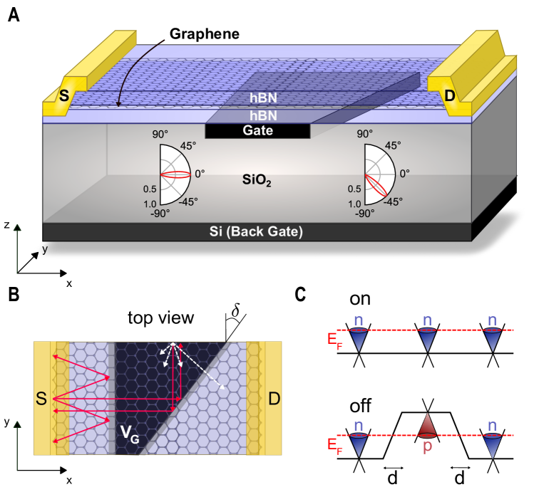
A perfect match of the pseudospin structure at the interface causes a GPNJ to become completely transparent to normally incident electrons (Klein tunneling Katsnelson et al. (2006); Young and Kim (2009)) while it becomes more opaque as the incident angle increases. Ramping up the voltage barrier across the junction collimates the electrons by narrowing the distribution of their transmission angles. This collimation can be further enhanced with a smoothly varying barrier of finite width spanning a split gated junction, which imposes an added Gaussian distribution around normal incidence Cheianov and Fal’ko (2006). Subsequently, putting a second junction at a relative angle () rejects most of the electrons as long as exceeds the maximum critical angle () of the filtered and collimated electrons Sajjad and Ghosh (2013). This two junction device, analogous to a polarizer/analyzer in optics, is broadly referred to as Graphene Klein Tunnel (GKT) transistor (Fig. 1).
Angle dependent transmission is key to getting a tunable resistance in a GKT, achieved by controlling the gate voltage. Sajjad et al. have shown that such a GKT transistor would show a clean transport gap in the off state leading to a nearly ideal transfer characteristic consisting of low off current, high
on-off ratio (==104) and steep subthreshold swing (SS) lower than the Boltzmann limit of 60 mV/decade Sajjad and Ghosh (2011, 2013). Beyond a desirable gate transfer characteristic, the GKT transistor was also shown to have an excellent output characteristic with a high saturating on current retaining a high mobility in the on state Elahi and Ghosh (2016); Tan et al. (2017). In these calculations Sajjad and Ghosh (2011, 2013); Elahi and Ghosh (2016) however, non-idealities such as momentum scattering, in particular at the edges were not considered.
Edge scattering of rejected electrons or holes at the second junction compromises the off state leakage current, as the charge carriers keep bouncing around until some of them find themselves in the narrow transmission lobe of the second junction. Indeed, considering edges and secondary bounces, a more realistic calculation using both quantum and semi-classical models showed that the on-off ratio degrades to 102 for perfect edges at widths of 1 m Jang et al. (2013); Wilmart et al. (2014); Elahi et al. (2017). Based on the initial two junction device idea Jang et al. (2013); Sajjad and Ghosh (2013), Morikawa et al. Morikawa et al. (2017) and Wang et al. Wang et al. (2018) reported experimental on-off ratios of 1.3 and 6-13 respectively, but these on-off ratios are low compared to predictions. Multiple experiments have now confirmed the basic physics of angle dependent transmission at a single tilted junction Sutar et al. (2012); Chen et al. (2016), and impact of Klein tunneling in a graphene quantum dot Gutiérrez et al. (2016), yet no rigorous study has been found explaining the poor on-off ratio in double junction devices in general.
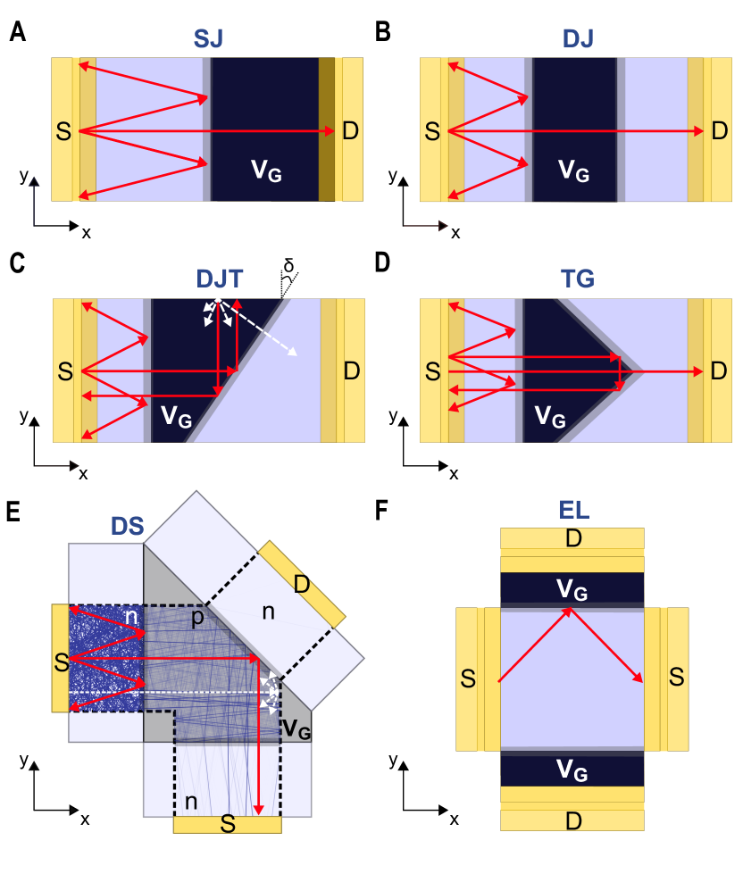
In this paper, we explain the existing discrepancy between simulations (on-off ratio 102) Jang et al. (2013); Wilmart et al. (2014); Elahi et al. (2017) and experiments (on-off ratio 10) Wang et al. (2018) of GKT devices. We find that in addition to the electrons suffering multiple bounces around the wedge shaped region between junctions, non-specular (diffusive) scattering by rough edges, shown by white arrow in Fig. 1B, plays an important role in degrading the on-off ratio by transforming the transport gap to a pseudogap with a non-zero floor (Fig. 2A). We study several variations of graphene p-n junction based devices. Starting from a basic building block, a single p-n junction, we extend to complex structures consisting of multiple junctions. Specifically, we consider a split-gated single junction (SJ), parallel split-gated dual junctions (DJ), two split-gated dual junctions in an angled trapezoidal geometry (DJT) Sajjad and Ghosh (2013), a triangular gated (TG) prism geometry (basic building block of saw-tooth geometry Jang et al. (2013); Wilmart et al. (2014)), a dual-source (DS) device Wang et al. (2018), and finally a structure with two drains rotated at 90∘ relative to two sources, generating an effective EdgeLess device (EL). In Fig. 3, all the structures are shown with their off state electron paths marked in red. Our comparative study shows advantages and disadvantages of one structure over another, providing a guideline for designing electron optics inspired devices in future.
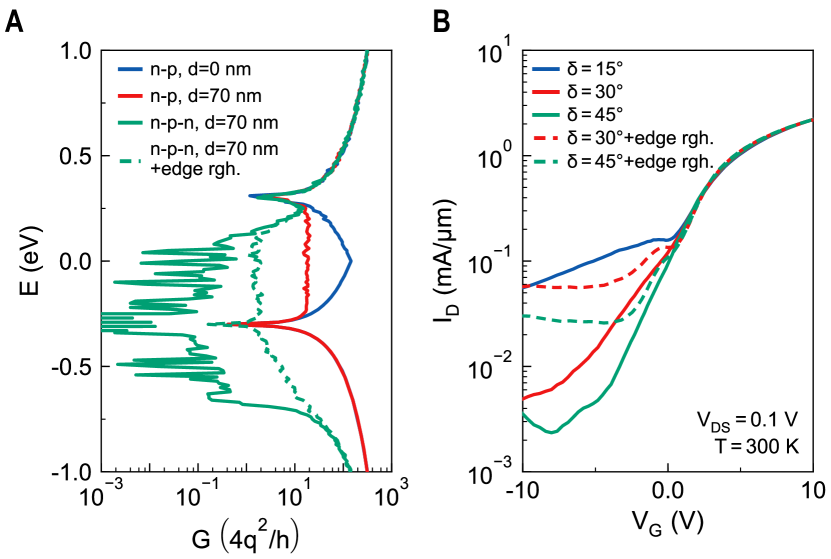
A finite transport gap generated by the angular filtering of electrons differentiates GKT devices from conventional graphene Field Effect Transistors (gFET). In Fig. 2A, we see a transport gap arising from the double junction structure (DJT). We also show the case for abrupt p-n junction ( = 0 nm) where filtering is not that robust. A smooth p-n junction ( = 70 nm) performs better than an abrupt one due to added Gaussian filtering due to angle-dependent tunneling. In presence of edge roughness, the transport gap turns into a gap with a nonzero floor and increases the overall off state conductance (Fig 2A). We see dips at eV due to Dirac points. As shown in Fig 2B, edge roughness degrades the off state performance (10 V) for any given . We also show that = 45∘ gives the lowest off current even in the presence of edge roughness, as suggested earlier Sajjad et al. (2012). Here, local gate dielectric (hexagonal boron nitride, hBN) thickness is 32 nm. To discuss the effect of edge roughness in detail as well as the dependence on device geometry, we analyze a variety of structures in this paper (Fig. 3).
In this study, we adopt semiclassical ray tracing approach Chen et al. (2016); Elahi et al. (2017) based on a billiard model Beenakker and Van Houten (1989); Milovanović et al. (2013, 2014) that has been benchmarked against experiments Chen et al. (2016). A charge carrier hitting a perfect edge reflects back with an angle equal to the incident angle (specular reflection). In presence of edge roughness, a Gaussian distributed random angle of reflection with standard deviation (higher denoting rougher edges) is added. The transmission probability () for each electron across a junction is calculated analytically, using a generalized version Sajjad and Ghosh (2013) (eqn. S1 SI (2)) of the well-known equation Cheianov and Fal’ko (2006) for symmetric junction, . Here, is the magnitude of the Fermi wave vector on each side for a symmetric p-n junction, is the junction width, and is the incident angle at the junction. We calculate channel resistance for low-bias and total resistance using , where is the contact resistance between graphene and source/drain electrodes SI (2). To explain experimental data Wang et al. (2018), contact resistance 100 -m and non-specular edge scattering are included in our semiclassical simulation model. The local gate dielectric (hBN) thickness is 32 nm, junction width is 70 nm, temperature is 50 K, and device width is 1 m unless otherwise mentioned. The main advantage of ray tracing over the Non-equilibrium Green’s function (NEGF) formalism is its computational practicality.
We now discuss the impact of gate geometry on various flavors of ballistic, perfect edge GKT transistors, as quantified by their low-bias resistances and on-off ratios. Figure 4A shows the results of the low-bias on and off state resistances for each geometry. The back gate voltage is kept fixed to =100 V (corresponding to charge density =6.631012 cm-2 for SiO2 thickness of 300 nm in addition to 32 nm hBN) for all these devices while we sweep the local gate to vary the corresponding charge density of middle gate region () from negative (p-type) to positive (n-type), giving us the off and on states respectively. Our first structure, an SJ device (Fig. 3A) filters out carriers at angles other than normal incidence, exhibiting Klein tunneling. Adding another junction aligned to the first one (Fig. 3B, DJ) does not help in increasing on-off ratio significantly, but instead adds another comparable resistance along the path. With a tilted second junction (Fig. 3C, DJT with ), we can achieve orders of magnitude larger off state resistance for ballistic flow. Next the TG device (Fig. 3D) uses the second junction to reflect back strongly collimated carriers towards the source away from the edges. However, it has a poorer performance in the off state than DJT structure because it allows electrons to Klein tunnel through its vertex on the first try. The DS device Wang et al. (2018) (Fig. 3E) has an overall L-shape, so that each segment of the split source recaptures carriers injected from the other segment and rejected by the tilted junction, without letting them bounce again at the edges. As a result, its off state performance is superior to the DJT device. Finally, the EL (Fig. 3F) device capitalizes on a structure that is free from edge effects. In the EL structure shown, electrons enter along one axis from both sources, while the drains are along a perpendicular axis with the gate induced p-n junctions sitting in between. Such EL structures reduce the off current because most electrons incident at the junction are at large angles. Compared to an ideal DJT device, the off state resistance is still low as it uses only one junction. Moreover, the on state current of the EL, determining its device speed, is compromised by the right angle separating source and drain - moving the drain away from the natural ‘line of sight’ of the injected source electrons. The low on current degrades the overall on-off ratio of the EL device.
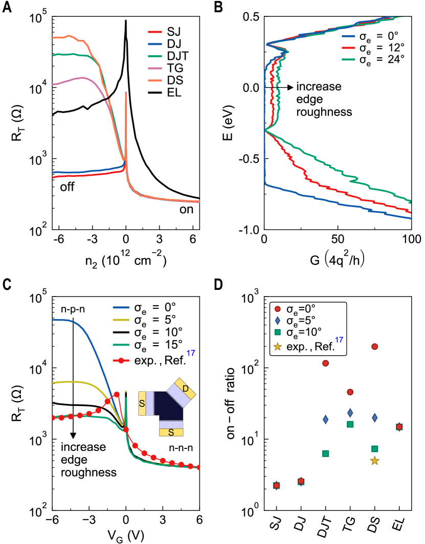
Edge roughness tends to decrease the on-off ratio of these devices by diffusive scattering of the reflected electrons providing a leakage path to the drain as shown in Fig. 3(C, E) by the white dashed lines. Thus the transport gap turns into a pseudo gap with a finite floor (Fig. 4B) with increasing edge roughness. For ideal edges we see a transport gap spanning -0.67 eV to +0.3 eV. With increasing edge roughness, the floor value of the gap also increases (other than at = -0.3 eV due to a clear Dirac point, which in turn could be washed out by impurity scattering and puddles Sajjad et al. (2015)), thus increasing off state conductance and decreasing resistance. In Fig. 4C, we show the evolution of resistance characteristics of the DS device with increasing edge roughness. Here we use device parameters = 60 nm, width=800 nm, and voltages 6 V to 6 V, = 60 V, emulating a local gate voltage of 6 V, as in the experiment Wang et al. (2018). In Ref. Wang et al. (2018), all the regions (n-n-n/n-p-n) are controlled by local gates whereas in our simulation only the middle region is controlled by a local gate () while other regions are controlled by back gate (). We match the on state ( = 6 V) result by fitting a contact resistance ( = 117 -m) and off state (6 V) resistance by fitting edge roughness parameter =15∘. We see a mismatch between our simulation and experiment at V due to charge puddles that average out the Dirac points Sajjad et al. (2015).
Figure 4D shows the evolution of the on-off ratio for all the device geometries in presence of edge roughness. We clearly see orders of magnitude enhancement of on-off ratio in DJT compared to SJ and DJ, but in the presence of edge roughness the on-off ratio degrades significantly. In contrast, although the TG device starts with a lower on-off ratio due to Klein tunneling at the vertex, it shows robustness against edge roughness as it directs the collimated electrons away from the edges (Fig. 3D). The DS device is supposed to perform better even in presence of edge roughness. However, as the device geometry Wang et al. (2018) is not optimized considering edge roughness (Fig. 3E, second junction position, electrons shown in white arrow hits edge), the on-off ratio degrades significantly. Improved device geometry (DS) shows at least 2 times better on-off ratio in presence of edge roughness (Fig. S1 SI (2)). In Fig. 4D, we also show the experimental on-off ratio Wang et al. (2018) from Fig. 4C, notably with different device width and doping than for simulation. Finally, the EL device which starts with an even lower on-off ratio than the TG device, but the on-off ratio remains constant with increasing edge roughness as the electrons do not hit any edge before getting filtered out.
As a transistor, a ballistic GKT greatly outperforms wave-guided structures based on the Veselago effect. However, even a GKT faces challenges arising from the presence of edges - in particular rough ones, together with contact resistance and finite doping of graphene by metal contacts. A 1 m wide structure with perfect edges is predicted to have a gate transfer characteristic with an on-off ratio 102, but current technology limits the edge smoothness and degrades the on-off ratio to 10, demonstrated experimentally Wang et al. (2018). Such a low on-off ratio is not yet suitable for digital logic.
The output characteristic, however, bears more promise. At high drain bias (), a small transport gap (n+-n-n+, on state) at energies far from the equilibrium Fermi level is predicted to produce a strongly saturating - that is robust against edge roughness Tan et al. (2017). Even cases with an on-off ratio 10 can result in an order of magnitude increment in (output resistance) without hurting the mobility. Devices like this with high mobility and output resistance can be quite useful for analog RF applications, delivering a high (unity current gain cutoff frequency) and (unity power gain cutoff frequency) Tan et al. (2017). To improve device performance, a superlattice potential may be incorporated into the device to create an anisotropic band structure and create a much more aggressive collimation of electrons Park et al. (2008); Forsythe et al. (2018). Further improvements may be possible with abrupt junctions if doping can be improved in the first region, so that the reflected electrons at the second junction are no longer stopped by an abrupt first junction on their way to the source (recall that total internal reflection only works one way like a diode, from a denser to a rarer medium). A major factor in determining the overall performance of all these structures is edge roughness, included here as a phenomenological parameter, the standard deviation of a Gaussian angular smear. The relationship between and physical roughness parameters, as well as decay rates extracted from magnetoconductance measurements is out of scope of this study and will be reported elsewhere.
In summary, the performance challenges of a GKT transistor are outlined in this paper. Although junction line-edge roughness Zhou et al. (2018) and other scattering events are expected to play a role, we focused here on edge roughness that is expected to be the most deleterious to the on-off ratio through momentum redirection. We quantified the role of graphene-edge roughness and attempted to design around it, such as the EL device. We analyzed a family of devices and find that TG, DS and EL device are less susceptible to edge roughness. We further showed that an angle of 45∘ between collimator and reflector gives the best performance even in the presence of edge roughness. Our analysis shows that even with geometry optimization the on-off ratio may not be enough for scaled digital switching, but may still offer advantages for high frequency RF analog applications Tan et al. (2017).
This work was supported by Semiconductor Research Corporation’s (SRC) NRI-INDEX center. The authors want to thank Cory R. Dean for important discussions.
References
- Williams et al. (2011) J. Williams, T. Low, M. Lundstrom, and C. Marcus, Nature Nanotechnology 6, 222 (2011).
- Sajjad and Ghosh (2011) R. N. Sajjad and A. W. Ghosh, Applied Physics Letters 99, 123101 (2011).
- Jang et al. (2013) M. S. Jang, H. Kim, Y.-W. Son, H. A. Atwater, and W. A. Goddard, Proceedings of the National Academy of Sciences 110, 8786 (2013).
- Sajjad and Ghosh (2013) R. N. Sajjad and A. W. Ghosh, ACS nano 7, 9808 (2013).
- Wilmart et al. (2014) Q. Wilmart, S. Berrada, D. Torrin, V. H. Nguyen, G. Fève, J.-M. Berroir, P. Dollfus, and B. Plaçais, 2D Materials 1, 011006 (2014).
- Morikawa et al. (2017) S. Morikawa, Q. Wilmart, S. Masubuchi, K. Watanabe, T. Taniguchi, B. Plaçais, and T. Machida, Semiconductor Science and Technology 32, 045010 (2017).
- Tan et al. (2017) Y. Tan, M. M. Elahi, H.-Y. Tsao, K. M. Habib, N. S. Barker, and A. W. Ghosh, Scientific reports 7, 9714 (2017).
- Ghosh (2015) A. W. Ghosh, IEEE Journal of the Electron Devices Society 3, 135 (2015).
- Cheianov et al. (2007) V. V. Cheianov, V. Fal’ko, and B. Altshuler, Science 315, 1252 (2007).
- Lee et al. (2015) G.-H. Lee, G.-H. Park, and H.-J. Lee, Nature Physics 11, 925 (2015).
- Low et al. (2009) T. Low, S. Hong, J. Appenzeller, S. Datta, and M. S. Lundstrom, IEEE Transactions on Electron Devices 56, 1292 (2009).
- Cheianov and Fal’ko (2006) V. V. Cheianov and V. I. Fal’ko, Physical review b 74, 041403 (2006).
- Katsnelson et al. (2006) M. Katsnelson, K. Novoselov, and A. Geim, Nature physics 2, 620 (2006).
- Young and Kim (2009) A. F. Young and P. Kim, Nature Physics 5, 222 (2009).
- Elahi and Ghosh (2016) M. M. Elahi and A. W. Ghosh, in Device Research Conference (DRC), 2016 74th Annual (IEEE, 2016) pp. 1–2.
- Elahi et al. (2017) M. M. Elahi, K. M. M. Habib, and A. W. Ghosh, in Energy Efficient Electronic Systems (E3S), 2017 Fifth Berkeley Symposium on (IEEE, 2017) pp. 1–3.
- Wang et al. (2018) K. Wang, M. M. Elahi, K. Habib, T. Taniguchi, K. Watanabe, A. W. Ghosh, G.-H. Lee, and P. Kim, arXiv preprint arXiv:1809.06757 (2018).
- Sutar et al. (2012) S. Sutar, E. Comfort, J. Liu, T. Taniguchi, K. Watanabe, and J. Lee, Nano letters 12, 4460 (2012).
- Chen et al. (2016) S. Chen, Z. Han, M. M. Elahi, K. M. Habib, L. Wang, B. Wen, Y. Gao, T. Taniguchi, K. Watanabe, J. Hone, et al., Science 353, 1522 (2016).
- Gutiérrez et al. (2016) C. Gutiérrez, L. Brown, C.-J. Kim, J. Park, and A. N. Pasupathy, Nature Physics 12, 1069 (2016).
- Sajjad et al. (2012) R. N. Sajjad, S. Sutar, J. Lee, and A. W. Ghosh, Physical Review B 86, 155412 (2012).
- Beenakker and Van Houten (1989) C. Beenakker and H. Van Houten, Physical review letters 63, 1857 (1989).
- Milovanović et al. (2013) S. Milovanović, M. Ramezani Masir, and F. Peeters, Applied Physics Letters 103, 233502 (2013).
- Milovanović et al. (2014) S. Milovanović, M. Ramezani Masir, and F. Peeters, Journal of Applied Physics 115, 043719 (2014).
- SI (2) Supplementary material for simulation details and double source geometry improvement.
- Sajjad et al. (2015) R. N. Sajjad, F. Tseng, M. Habib, and A. W. Ghosh, Phys. Rev. B 92, 205408 (2015).
- Park et al. (2008) C.-H. Park, L. Yang, Y.-W. Son, M. L. Cohen, and S. G. Louie, Nature Physics 4, 213 (2008).
- Forsythe et al. (2018) C. Forsythe, X. Zhou, K. Watanabe, T. Taniguchi, A. Pasupathy, P. Moon, M. Koshino, P. Kim, and C. R. Dean, Nature nanotechnology , 1 (2018).
- Zhou et al. (2018) X. Zhou, A. Kerelsky, M. M. Elahi, D. Wang, K. Habib, R. N. Sajjad, P. Agnihotri, J. U. Lee, A. W. Ghosh, F. M. Ross, et al., arXiv preprint arXiv:1810.02308 (2018).
Supplementary Material for
Impact of geometry and non-idealities on electron ‘optics’ based graphene p-n junction devices
Mirza M. Elahi,1,a) K. M. Masum Habib,1,b) Ke Wang,2,3 Gil-Ho Lee,2,4 Philip Kim,2 Avik W. Ghosh1,5
1Department of Electrical and Computer Engineering, University of Virginia, Charlottesville, Virginia 22904, USA.
2Department of Physics, Harvard University, Cambridge, MA 02138, USA.
3School of Physics and Astronomy, University of Minnesota, Minneapolis, MN 55455, USA.
4Department of Physics, Pohang University of Science and Technology, Pohang 37673, South Korea.
5Department of Physics, University of Virginia, Charlottesville, VA 22904, USA.
a)Electronic mail: me5vp@virginia.edu
b)Present address: Present address: Intel Corp., Santa Clara, CA 95054, USA.
S1 Simulation method
Semiclassical ray tracing model relies on the assumption that the most relevant quantum effects in GKT devices manifest during tunneling at the junctions, while for large-scale devices with rough edges, interference effects are expected to be washed out under the gated regions. Accordingly, we throw electrons from a source with random injection angles following a cosine distribution function Molenkamp et al. (1990), and evolve each electronic trajectory with constant speed (Fermi velocity) and band effective mass, following classical trajectories. The transmission probability () of electrons at the junction is calculated [4, 21] using
| (S1) |
where, and are the incident and refraction angle, is the critical angle from Snell’s Law, is the junction width, and and are the Fermi wave vectors on the incident and transmitted side respectively.
Assuming non-interacting charge carriers, we consider a fraction of each electron at the junction that passes through, while a fraction is reflected back to the incident region. The trajectories of the reflected and transmitted fractional electrons are allowed to evolve once again through multiple such transmission-reflection events until they end up either at the source or the drain. The average transmission probability () from contact to contact is calculated by counting electrons () that eventually make it to the contact for a given total number of carriers injected from contact . Thereafter the Landauer-Büttiker formalism at low-bias is used to calculate channel conductance () by summing up the terminal transmissions.
| (S2) |
where is the Fermi energy, is the number of modes, is the sum over all transmissions, and is the equilibrium Fermi function.
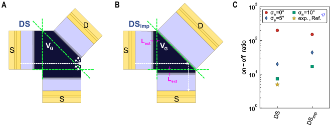
S2 Geometry improvement of Double Source (DS) device
The main motivation behind DS device in Ref. [17] was to use only junction in filtering procedure at the local gated region. In Fig. S1A, we can clearly see that this region is not free from edges and can be further optimized. Fig. S1B shows the structure (DS) to improve the device performance in presence of edge roughness. is kept to have feasible smooth electrostatics for both junction and reduce leakage path at the corners. Figure S1C shows comparison between DS and DS structure in terms of on-off ratio and we clearly see that DS is less sensitive to edge roughness.
References
- Molenkamp et al. (1990) L. Molenkamp, A. Staring, C. Beenakker, R. Eppenga, C. Timmering, J. Williamson, C. Harmans, and C. Foxon, Physical Review B 41, 1274 (1990).