CMOS-Integrated Diamond Nitrogen-Vacancy Quantum Sensor
Abstract
The nitrogen vacancy (NV) center in diamond has emerged as a leading solid-state quantum sensor for applications including magnetometry, electrometry, thermometry, and chemical sensing. However, an outstanding challenge for practical applications is that existing NV-based sensing techniques require bulky and discrete instruments for spin control and detection. Here, we address this challenge by integrating NV based quantum sensing with complementary metal-oxide-semiconductor (CMOS) technology. Through tailored CMOS-integrated microwave generation and photodetection, this work dramatically reduces the instrumentation footprint for quantum magnetometry and thermometry. This hybrid diamond-CMOS integration enables an ultra-compact and scalable platform for quantum sensing and quantum information processing.
Quantum metrology based on solid-state spins has shown outstanding sensing capabilities for various environmental physical quantities. In particular, the NV center in diamond has emerged as a leading room-temperature quantum sensor for temperature1; 2; 3; 4, strain5; 6; 7, electric fields8; 9; 10, and magnetic fields11; 12; 13; 14; 15; 16; 17 especially to determine atomic species 18; 19; 20; 21; 22; 23; 24; 25. The advances of NV-based quantum metrology are based on its long spin coherence time26 and its efficient optical interface for spin polarization and readout. Furthermore, picotesla magnetic field sensitivity at DC under ambient conditions has been achieved27 by interrogating NV center ensembles. This hybrid NV-CMOS platform is a highly advanced, scalable and compact platform for quantum sensing and will serve as a foundation for a new class of quantum systems.
Conventional approaches for NV magnetometry based on optically detected magnetic resonance (ODMR)28 involve discrete off-the-shelf instruments that limit practical applications and scalability. NV ODMR requires (i) a microwave signal generator, amplifier, and delivery interface for NV spin manipulation, (ii) an optical filter to reject the pump laser, (iii) a photodetector for NV spin-dependent fluorescence measurement, and (iv) a pump laser. The use in conventional quantum sensing experiments of bulky instruments makes NV magnetometry hard outside of the lab or within mobile devices.
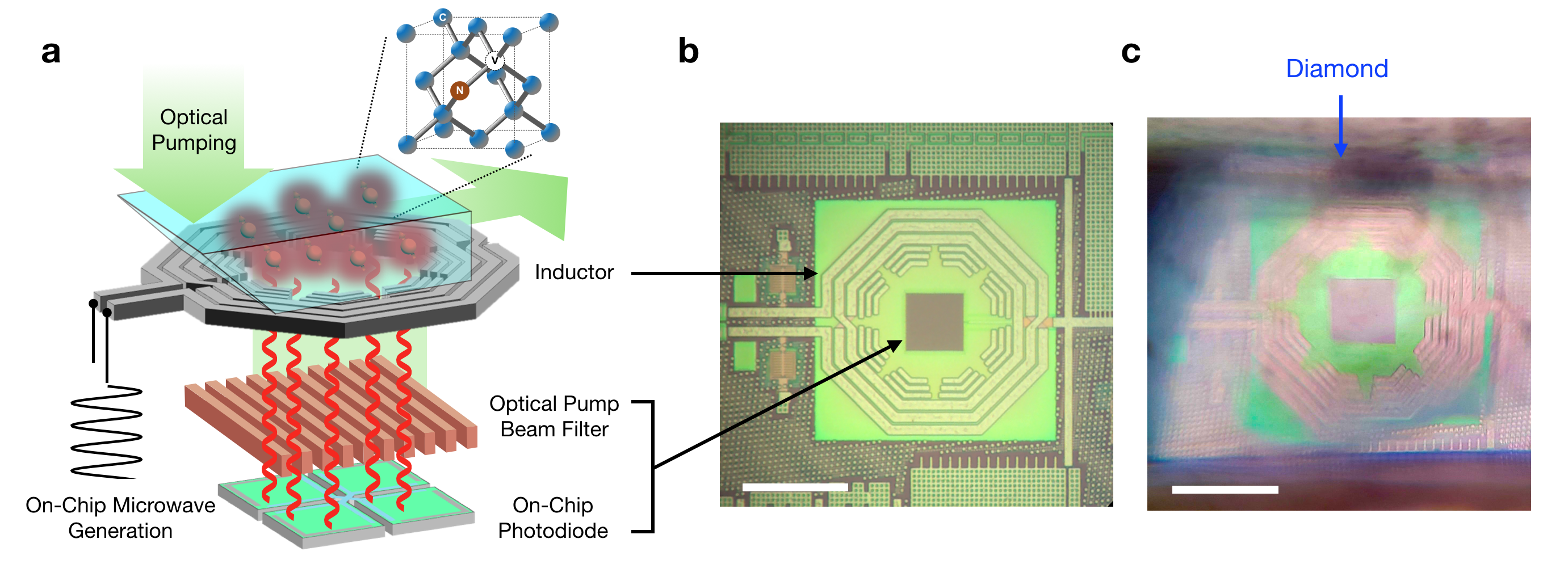
Here, we realize a custom CMOS architecture that integrates requirements (i-iii) directly with a diamond sensor. This architecture29 stacks the microwave inductor, filter, and photodiode into a 200 m 200 m footprint. We use this hybrid diamond-CMOS platform to demonstrate ambient quantum magnetometry and thermometry.
Chip-Scale Quantum Sensing
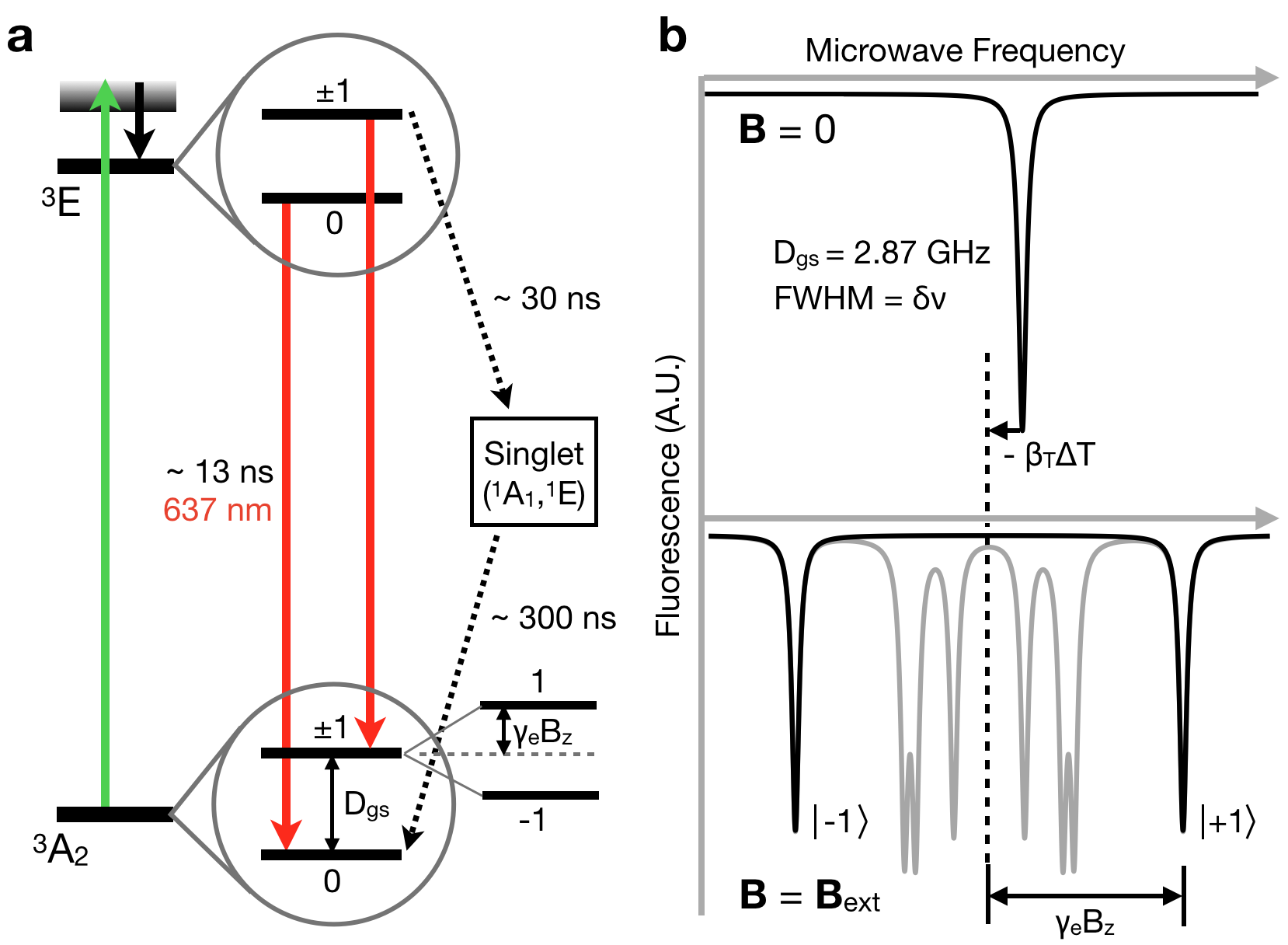
Figure 1a illustrates the device for on-chip ODMR. A diamond slab is irradiated and annealed to produce NV centers at a density of . A 45∘ cut in the corner of the diamond directs the off-chip green pump beam along the length of the diamond slab. This side-excitation reduces pump laser background into the photodetector located below the diamond. An on-chip microwave generator and inductor drives the NV electron spin transitions.
NV magnetometry detects external magnetic fields through the Zeeman shift induced on the NV’s spin ground state sublevels28, shown in Fig. 2a. Specifically, an external magnetic field induces an energy shift on the NV ground state spin triplet (), where is the magnetic field component along the NV symmetry axis. The spin transition frequencies, , between sublevels and , are given by
| (1) |
where is the room-temperature natural ground-state splitting between sublevels and , is the electronic gyromagnetic ratio (), 30, and is the temperature shift from room temperature. Measuring gives and in their difference and sum, respectively. In addition, measuring for at least three of the four possible NV orientations in diamond (Inset in Fig. 1a) quantifies all components of for vector magnetometry31; 32; 33; 34.
The NV ground state transitions are measured by ODMR under green laser excitation, as illustrated in Fig. 2a. The spin magnetic sublevel has a bright cycling transition, where it emits red fluorescence. In contrast, the can undergo an intersystem crossing into a metastable, dark spin-singlet state, from where it decays back into the sublevel. This has two consequences: optical spin polarization into sublevel and lower average fluorescence of the spin populations. The microwave field moves spin population between and . Sweeping the applied microwave frequency leads to the ODMR spectra in Fig. 2b, from which are determined.
On-Chip microwave Generation and Delivery
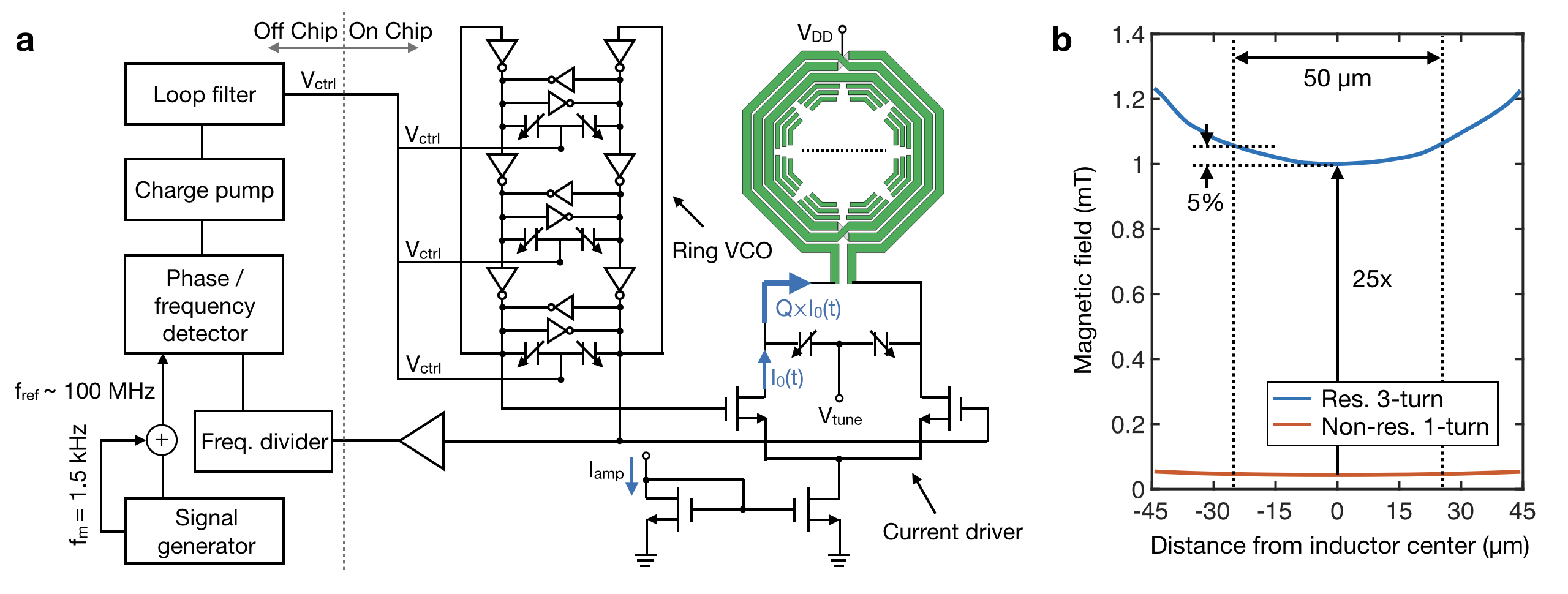
In our chip-scale NV magnetometer, the ground-state spin transitions are driven by the on-chip generated microwave fields. Figure 3a shows the circuitry for on-chip microwave generation and delivery. This circuitry is composed of a frequency synthesis loop, a current driver, and a resonant loop inductor. The frequency synthesis loop generates the microwave sweep signal from 2.6 GHz to 3.1 GHz required for the ODMR experiment. The main component of this loop is the on-chip CMOS ring voltage controlled oscillator (VCO). The ring VCO has a wide tuning range and avoids inductors35, which minimizes the cross-talk between the oscillator and the microwave inductor which drives the NV ensemble. The loop is closed with off-chip components to enhance the stability and decrease the phase noise of the signal.
The microwave fields are delivered to the NV ensemble through the loop inductor (Fig. 3a) implemented on the top most metal layer (Metal 9). To efficiently deliver microwave field, the loop inductor and a pair of shunt capacitors form a resonating load for the current driver. The load resonates near . This current driver is fed by the output of the ring VCO. Therefore, the current flowing in the inductor is at the microwave frequency. To improve the performance of this inductor for advanced NV sensing protocols we wish to increase the emitted MW field amplitude36. The amplitude is enhanced by a factor Q of the driver DC bias current ( ), where Q () is the quality factor of the inductor. In addition, we use a three-turn loop to multiply the microwave field strength. Overall, we have enhanced microwave field strength compared to a non-resonant single turn loop (as plotted in Fig. 3b). These protocols also require highly uniform microwave fields over the excitation volume. To achieve this, three capacitive parasitic loops are inserted29. We tailor the radius of the these loops, so that their opposite induced field homogenize the overall generated field. Another degree of freedom is the capacitive gaps in the parasitic loops. This controls the amount of current flowing in these loops. Therefore, we optimized these two parameters (i.e. the parasitic loop radius and the capacitive gap) for the three parasitic loops to achieve uniformity.
On-chip Spin Readout
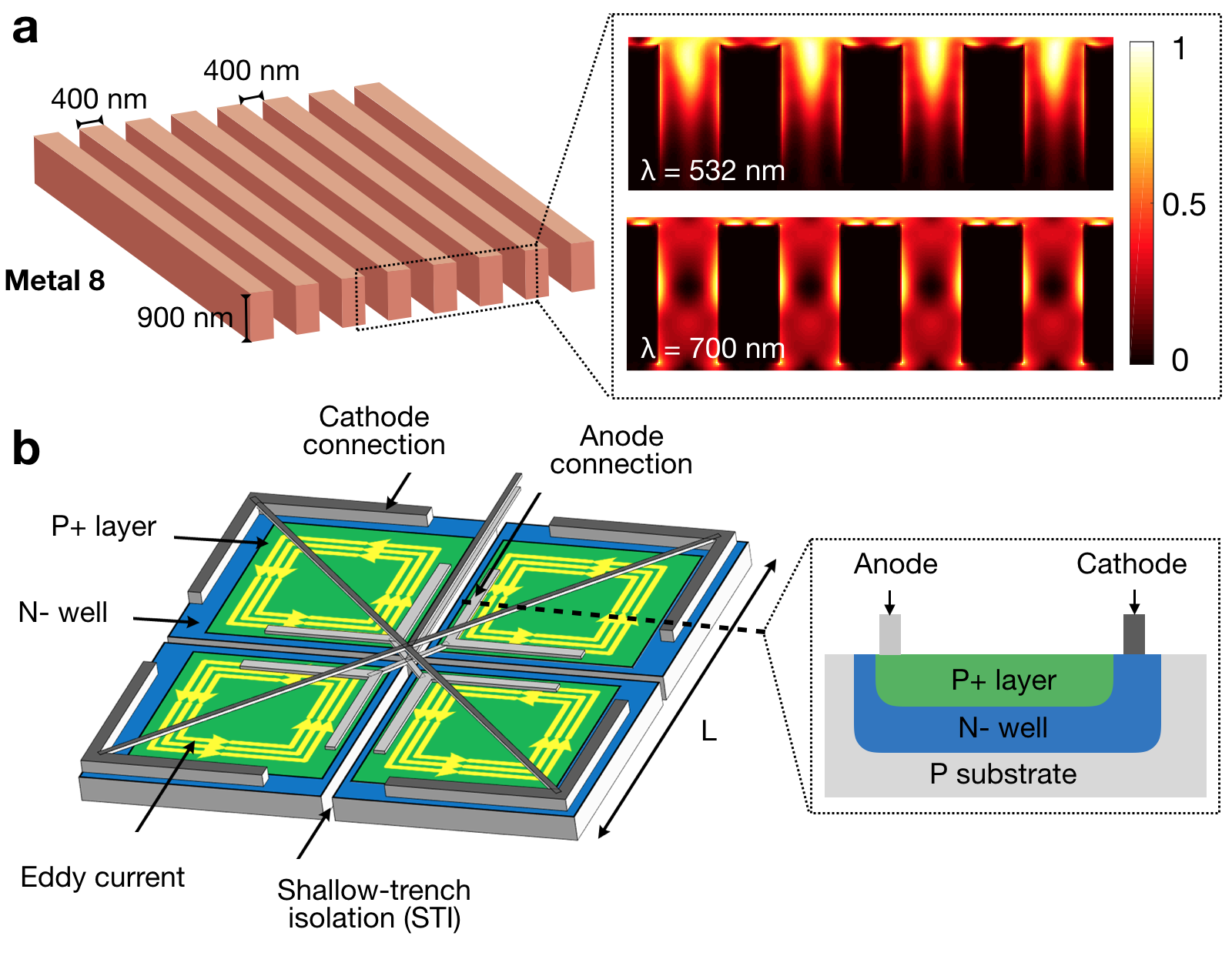
The NV spin transitions are detected using an on-chip photodetector. A CMOS-compatible periodic metal-dielectric structure (Fig. 4a) in the Metal 8 interconnect layer filters green pump light. Specifically, incident light couples to the surfacepplasmon polariton (SPP) at the metal-dielectric interface, where green light rapidly decays due to frequency-dependent Ohmic loss37; 38. The inset in Fig. 4a plots the intensity map for the green (, Top) and red light (, Bottom), showing the and absorption for green and red light through the structure, respectively.
The photodiode consists of a P+/N-well/P-sub junctions (Inset in Fig. 4b), which is preferable for long wavelength detection39. Since we place the photodiode with its conductive layers below the inductor (Fig. 1a), large eddy currents near 2.87 GHz can be induced. This reduces the quality factor of the inductor, resulting in microwave amplitude reduction. We reduce this eddy current by half, by dividing the photodiode area into four subareas as shown in Fig. 4b (See Methods for detailed analysis). Furthermore, the anode/cathode connectors are arranged in a similar way to patterned ground shielding used in CMOS inductors40. This arrangement avoids any closed loops, which helps to cut the eddy current that may flow in the metallic connections. The photodiode has a measured responsivity of 0.23 A/W at the wavelength of 532 nm and a noise-equivalent-power of at 1.5 kHz.
Experimental Results
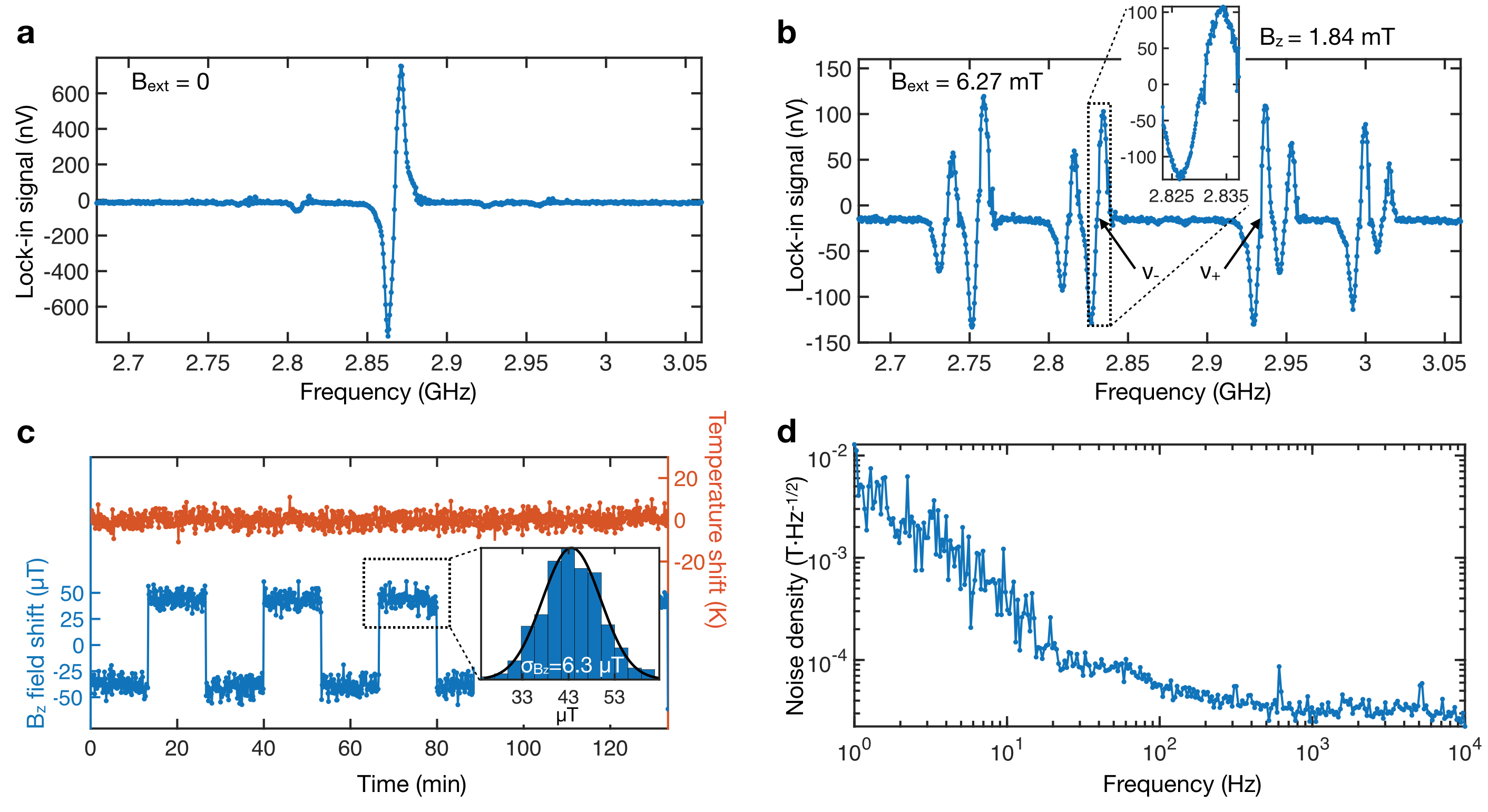
We detect NV-ODMR with a lock-in technique. The green laser beam continuously excites the NV ensemble, and the frequency-modulated (FM) microwave fields ( and modulation depth of 6 MHz) drive the NV electron spin transition. The spin-dependent fluorescence produces photo-current within the on-chip photodiode (Fig. 4b). Then, we read out the modulated photo-current at within an bandwidth of 0.078 Hz (a time constant of 1 second, considering the 24 dB/oct roll-off) with a lock-in amplifier (SR865A, Stanford Research System).
Figure 5a shows the lock-in signal for the ODMR experiment under zero external magnetic field applied. This spectrum corresponds to the derivative of the ODMR spectrum shown in Fig. 2b. Next, we align a permanent magnet (6.27 mT) to split the spin transitions of the four NV orientations. Figure 5b shows the ODMR spectrum, which exhibits the expected eight spin transitions (Fig. 2b). In particular, we note the spin transitions at and of the NV ensemble.
Monitoring the lock-in signal at and allows independent measurements of magnetic field and temperature, as described above. Specifically, the sum of the lock-in signal change at is proportional to , while the difference provides :
| (2) |
and
| (3) |
Figure 5c plots the detected induced by an electromagnet (blue) and measured (red).
The magnetic field sensitivity is given by the following relation:
| (4) |
Here, is the noise in measurement, and ENBW is the equivalent noise bandwidth of the lock-in detector. In our measurement, with a time constant of 1 second, accounting for the of the lock-in amplifier roll-off. By measuring of (Inset in Fig. 5c), we determine our DC magnetic field sensitivity of 32.1 T with a lock-in frequency of 1.5 kHz. Figure 5d plots the magnetic noise density measured at (no temperature compensation) with the noise floor of T.
Discussion
The magnetic field sensitivity of our magnetometer is mainly limited by the green laser. Improving the on-chip optical filter performance by additional 60 dB (including nanophotonic structures41 in diamond or using multiple metal layers in CMOS) can improve the sensitivity by three orders of magnitude. In addition, recycling the green optical pump beam with a diamond wave-guide geometry27, and implementing dynamical decoupling techniques28; 36 would also lead to orders of magnitude sensitivity improvements.
In conclusion, we demonstrate chip-scale quantum magnetometry by integrating diamonds with CMOS technology. Throughout the CMOS multi-layers, essential components to detect NV ODMR - a microwave generator, an inductor, an optical pump beam filter, and a photodetector - are fabricated. NV spin ensembles integrated on the CMOS chip measure external magnetic fields with the sensitivity of 32.1 T/. This compact spin-CMOS platform can be extended toward on-chip sensing of other quantities such as electric fields. We emphasize that the CMOS circuit in this work provides direct physical interactions with the NV quantum states beyond electronic I/O signaling42.
In addition to chip-scale quantum sensing capability, our CMOS-based spin control and readout scheme will uniquely provide a scalable solution for implementing spin quantum-bit controls. This is in particular essential to develop a large-scale quantum information processor43; 44; 42; 45, which enables quantum enhanced sensing46; 47; 36 and quantum information processing 48; 49; 50.
Methods
Diamond and CMOS Preparation
To avoid the direct injection of the green laser pump beam on the CMOS, we cut the CVD-grown diamond single crystal (Element 6) as shown in Fig. 1a, which enables the optical pumping in parallel with the CMOS-diamond interface with total internal reflection. This diamond is irradiated by the electron beam with a dosage of at 1 MeV. Then, the diamond is annealed for 2 hours at 850∘ Celsius. Our CMOS chip is fabricated with 65 nm LP TSMC technology. To reduce the background red fluorescence from the CMOS passivation layer, we etched the layer with plasma reactive-ion.
Measurement Setup
A linearly polarized DPSS green laser beam (500 mW, , Verdi G2, Coherent) is delivered to the diamond through a telescope of and . The beam diameter incident on the diamond is . A half-wave plate rotates the polarization of the laser beam to maximize the laser absorption through the periodic metal/dielectric structure in the Metal 8 layer. A permanent magnetic was used in Fig. 5b to split the NV orientations. The square-wave magnetic field applied in Fig. 5c was generated by an electromagnet. Alternating electrical current was used to avoid magnetization.
Eddy Current Analysis
For a square photodiode with a side length of L, the eddy current power is quadratically proportional to the change of the magnetic flux :
Here, is the time; is the resistance; and is the magnetic field generated by the loop inductor in Metal 9. By dividing the photodiode active area into by subareas, the eddy current is reduced by .
Acknowledgements
This research is supported in part by the Army Research Office Multidisciplinary University Research Initiative (ARO MURI) biological transduction program. D.K. acknowledges financial support from the Kwanjeong Educational Foundation. M.I. acknowledges support from Singaporean-MIT Research Alliance (SMART), and MIT Center of Integrated Circuits and Systems. C.F. acknowledges support from Master Dynamic Limited. M.T. acknowledges support by an appointment to the Intelligence Community Postdoctoral Research Fellowship Program at MIT, administered by Oak Ridge Institute for Science and Education through an interagency agreement between the U.S. Department of Energy and the Office of the Director of National Intelligence.
Author Contributions
D.E. and R.H. initially conceived the diamond-CMOS integration. M.I. conceived the idea of stacking the microwave inductor, plasmonic filter, and photodiode in a 3D architecture. M.I., C.F., and D.K. contributed to chip specifications, design and the experiment. M.I. constructed the CMOS chip prototype. D.K. performed FDTD simulation for the optical filter design and the diamond transfer on the CMOS chip. C.F. prepared the control software for the experiment. C.F. and D.K. constructed the optical setup and etched CMOS passivation layers. All authors contributed to the discussion of the experimental results and writing the manuscript.
Competing Interests
The chip-scale spin control and detection scheme in this work was filed as a United States Provisional Patent Application (62/623151).
Materials and Correspondence
The correspondence should be addressed to Ruonan Han (ruonan@mit.edu) or Dirk R. Englund (englund@mit.edu)
References
- Kucsko et al. (2013) Georg Kucsko, PC Maurer, Norman Ying Yao, Michael Kubo, HJ Noh, PK Lo, Hongkun Park, and Mikhail D Lukin, “Nanometre-scale thermometry in a living cell,” Nature 500, 54 (2013).
- Neumann et al. (2013) Philipp Neumann, Ingmar Jakobi, Florian Dolde, Christian Burk, Rolf Reuter, Gerald Waldherr, Jan Honert, Thomas Wolf, Andreas Brunner, Jeong Hyun Shim, et al., “High-precision nanoscale temperature sensing using single defects in diamond,” Nano letters 13, 2738–2742 (2013).
- Plakhotnik et al. (2014) Taras Plakhotnik, Marcus W Doherty, Jared H Cole, Robert Chapman, and Neil B Manson, “All-optical thermometry and thermal properties of the optically detected spin resonances of the nv–center in nanodiamond,” Nano letters 14, 4989–4996 (2014).
- Laraoui et al. (2015) Abdelghani Laraoui, Halley Aycock-Rizzo, Yang Gao, Xi Lu, Elisa Riedo, and Carlos A Meriles, “Imaging thermal conductivity with nanoscale resolution using a scanning spin probe,” Nature communications 6, 8954 (2015).
- Ovartchaiyapong et al. (2014) Preeti Ovartchaiyapong, Kenneth W Lee, Bryan A Myers, and Ania C Bleszynski Jayich, “Dynamic strain-mediated coupling of a single diamond spin to a mechanical resonator,” Nature communications 5, 4429 (2014).
- Teissier et al. (2014) J Teissier, A Barfuss, P Appel, E Neu, and P Maletinsky, “Strain coupling of a nitrogen-vacancy center spin to a diamond mechanical oscillator,” Physical review letters 113, 020503 (2014).
- Trusheim and Englund (2016) Matthew E Trusheim and Dirk Englund, “Wide-field strain imaging with preferentially aligned nitrogen-vacancy centers in polycrystalline diamond,” New Journal of Physics 18, 123023 (2016).
- Dolde et al. (2011) Florian Dolde, Helmut Fedder, Marcus W Doherty, Tobias Nöbauer, Florian Rempp, Gopalakrishnan Balasubramanian, Thomas Wolf, Friedemann Reinhard, Lloyd CL Hollenberg, Fedor Jelezko, et al., “Electric-field sensing using single diamond spins,” Nature Physics 7, 459 (2011).
- Chen et al. (2017) Edward H Chen, Hannah A Clevenson, Kerry A Johnson, Linh M Pham, Dirk R Englund, Philip R Hemmer, and Danielle A Braje, “High-sensitivity spin-based electrometry with an ensemble of nitrogen-vacancy centers in diamond,” Physical Review A 95, 053417 (2017).
- Broadway et al. (2018) D. A. Broadway, N. Dontschuk, A. Tsai, S. E. Lillie, C. T. K. Lew, J. C. McCallum, B. C. Johnson, M. W. Doherty, A. Stacey, L. C. L. Hollenberg, and J. P. Tetienne, “Spatial mapping of band bending in semiconductor devices using in situ quantum sensors,” Nature Electronics 1, 502–507 (2018).
- Maze et al. (2008) JR Maze, PL Stanwix, JS Hodges, S Hong, JM Taylor, P Cappellaro, L Jiang, MV Gurudev Dutt, E Togan, AS Zibrov, et al., “Nanoscale magnetic sensing with an individual electronic spin in diamond,” Nature 455, 644 (2008).
- Balasubramanian et al. (2008) Gopalakrishnan Balasubramanian, IY Chan, Roman Kolesov, Mohannad Al-Hmoud, Julia Tisler, Chang Shin, Changdong Kim, Aleksander Wojcik, Philip R Hemmer, Anke Krueger, et al., “Nanoscale imaging magnetometry with diamond spins under ambient conditions,” Nature 455, 648 (2008).
- Grinolds et al. (2014) MS Grinolds, M Warner, Kristiaan De Greve, Yuliya Dovzhenko, L Thiel, Ronald Lee Walsworth, S Hong, P Maletinsky, and Amir Yacoby, “Subnanometre resolution in three-dimensional magnetic resonance imaging of individual dark spins,” Nature nanotechnology 9, 279 (2014).
- Jensen et al. (2014) Kasper Jensen, Nathan Leefer, Andrey Jarmola, Yannick Dumeige, Victor M Acosta, Pauli Kehayias, Brian Patton, and Dmitry Budker, “Cavity-enhanced room-temperature magnetometry using absorption by nitrogen-vacancy centers in diamond,” Physical review letters 112, 160802 (2014).
- Wolf et al. (2015) Thomas Wolf, Philipp Neumann, Kazuo Nakamura, Hitoshi Sumiya, Takeshi Ohshima, Junichi Isoya, and Jörg Wrachtrup, “Subpicotesla diamond magnetometry,” Physical Review X 5, 041001 (2015).
- Glenn et al. (2015) David R Glenn, Kyungheon Lee, Hongkun Park, Ralph Weissleder, Amir Yacoby, Mikhail D Lukin, Hakho Lee, Ronald L Walsworth, and Colin B Connolly, “Single-cell magnetic imaging using a quantum diamond microscope,” Nature methods 12, 736 (2015).
- Boss et al. (2017) Jens M Boss, KS Cujia, Jonathan Zopes, and Christian L Degen, “Quantum sensing with arbitrary frequency resolution,” Science 356, 837–840 (2017).
- Mamin et al. (2013) HJ Mamin, M Kim, MH Sherwood, CT Rettner, K Ohno, DD Awschalom, and D Rugar, “Nanoscale nuclear magnetic resonance with a nitrogen-vacancy spin sensor,” Science 339, 557–560 (2013).
- Staudacher et al. (2013) Tobias Staudacher, Fazhan Shi, S Pezzagna, Jan Meijer, Jiangfeng Du, Carlos A Meriles, Friedemann Reinhard, and Joerg Wrachtrup, “Nuclear magnetic resonance spectroscopy on a (5-nanometer) 3 sample volume,” Science 339, 561–563 (2013).
- Häberle et al. (2015) T Häberle, D Schmid-Lorch, F Reinhard, and J Wrachtrup, “Nanoscale nuclear magnetic imaging with chemical contrast,” Nature nanotechnology 10, 125 (2015).
- Rugar et al. (2015) D Rugar, HJ Mamin, MH Sherwood, M Kim, CT Rettner, K Ohno, and DD Awschalom, “Proton magnetic resonance imaging using a nitrogen–vacancy spin sensor,” Nature nanotechnology 10, 120 (2015).
- Aslam et al. (2017) Nabeel Aslam, Matthias Pfender, Philipp Neumann, Rolf Reuter, Andrea Zappe, Felipe Fávaro de Oliveira, Andrej Denisenko, Hitoshi Sumiya, Shinobu Onoda, Junichi Isoya, et al., “Nanoscale nuclear magnetic resonance with chemical resolution,” Science 357, 67–71 (2017).
- Lovchinsky et al. (2016) Igor Lovchinsky, AO Sushkov, E Urbach, NP de Leon, Soonwon Choi, Kristiaan De Greve, R Evans, R Gertner, E Bersin, C Müller, et al., “Nuclear magnetic resonance detection and spectroscopy of single proteins using quantum logic,” Science 351, 836–841 (2016).
- Lovchinsky et al. (2017) Igor Lovchinsky, JD Sanchez-Yamagishi, EK Urbach, S Choi, S Fang, TI Andersen, K Watanabe, T Taniguchi, A Bylinskii, E Kaxiras, et al., “Magnetic resonance spectroscopy of an atomically thin material using a single-spin qubit,” Science , eaal2538 (2017).
- Glenn et al. (2018) David R Glenn, Dominik B Bucher, Junghyun Lee, Mikhail D Lukin, Hongkun Park, and Ronald L Walsworth, “High-resolution magnetic resonance spectroscopy using a solid-state spin sensor,” Nature 555, 351 (2018).
- Balasubramanian et al. (2009) Gopalakrishnan Balasubramanian, Philipp Neumann, Daniel Twitchen, Matthew Markham, Roman Kolesov, Norikazu Mizuochi, Junichi Isoya, Jocelyn Achard, Johannes Beck, Julia Tissler, et al., “Ultralong spin coherence time in isotopically engineered diamond,” Nature materials 8, 383 (2009).
- Clevenson et al. (2015) Hannah Clevenson, Matthew E Trusheim, Carson Teale, Tim Schröder, Danielle Braje, and Dirk Englund, “Broadband magnetometry and temperature sensing with a light-trapping diamond waveguide,” Nature Physics 11, 393 (2015).
- Taylor et al. (2008) JM Taylor, P Cappellaro, L Childress, L Jiang, D Budker, PR Hemmer, A Yacoby, R Walsworth, and MD Lukin, “High-sensitivity diamond magnetometer with nanoscale resolution,” Nature Physics 4, 810 (2008).
- Ibrahim et al. (2018) Mohamed I. Ibrahim, Christopher Foy, Donggyu Kim, Dirk R. Englund, and Ruonan Han, “Room-temperature quantum sensing in cmos: On-chip detection of electronic spin states in diamond color centers for magnetometry,” IEEE VLSI Circuits Symposium (2018).
- Acosta et al. (2010) VM Acosta, E Bauch, MP Ledbetter, A Waxman, L-S Bouchard, and D Budker, “Temperature dependence of the nitrogen-vacancy magnetic resonance in diamond,” Physical review letters 104, 070801 (2010).
- Maertz et al. (2010) BJ Maertz, AP Wijnheijmer, GD Fuchs, ME Nowakowski, and DD Awschalom, “Vector magnetic field microscopy using nitrogen vacancy centers in diamond,” Applied Physics Letters 96, 092504 (2010).
- Wang et al. (2015) Pengfei Wang, Zhenheng Yuan, Pu Huang, Xing Rong, Mengqi Wang, Xiangkun Xu, Changkui Duan, Chenyong Ju, Fazhan Shi, and Jiangfeng Du, “High-resolution vector microwave magnetometry based on solid-state spins in diamond,” Nature communications 6, 6631 (2015).
- Clevenson et al. (2018) Hannah Clevenson, Linh M Pham, Carson Teale, Kerry Johnson, Dirk Englund, and Danielle Braje, “Robust high-dynamic-range vector magnetometry with nitrogen-vacancy centers in diamond,” Applied Physics Letters 112, 252406 (2018).
- Schloss et al. (2018) Jennifer M Schloss, John F Barry, Matthew J Turner, and Ronald L Walsworth, “Simultaneous broadband vector magnetometry using solid-state spins,” arXiv preprint arXiv:1803.03718 (2018).
- Razavi (1998) Behzad Razavi, RF microelectronics, Vol. 2 (Prentice Hall New Jersey, 1998).
- Degen et al. (2017) Christian L Degen, F Reinhard, and P Cappellaro, “Quantum sensing,” Reviews of modern physics 89, 035002 (2017).
- Zayats et al. (2005) Anatoly V Zayats, Igor I Smolyaninov, and Alexei A Maradudin, “Nano-optics of surface plasmon polaritons,” Physics reports 408, 131–314 (2005).
- Hong et al. (2017) Lingyu Hong, Hao Li, Haw Yang, and Kaushik Sengupta, “Fully integrated fluorescence biosensors on-chip employing multi-functional nanoplasmonic optical structures in cmos,” IEEE Journal of Solid-State Circuits 52, 2388–2406 (2017).
- Murari et al. (2009) Kartikeya Murari, Ralph Etienne-Cummings, Nitish Thakor, and Gert Cauwenberghs, “Which photodiode to use: a comparison of cmos-compatible structures,” IEEE sensors journal 9, 752–760 (2009).
- Yue and Wong (1998) C Patrick Yue and S Simon Wong, “On-chip spiral inductors with patterned ground shields for si-based rf ics,” IEEE Journal of solid-state circuits 33, 743–752 (1998).
- Peng and Morris (1996) Song Peng and G Michael Morris, “Resonant scattering from two-dimensional gratings,” JOSA A 13, 993–1005 (1996).
- Charbon et al. (2017) Edoardo Charbon, Fabio Sebastiano, Masoud Babaie, Andrei Vladimirescu, Mina Shahmohammadi, Robert Bogdan Staszewski, Harald AR Homulle, Bishnu Patra, Jeroen PG Van Dijk, Rosario M Incandela, et al., “15.5 cryo-cmos circuits and systems for scalable quantum computing,” in Solid-State Circuits Conference (ISSCC), 2017 IEEE International (Ieee, 2017) pp. 264–265.
- Yao et al. (2012) Norman Y Yao, Liang Jiang, Alexey V Gorshkov, Peter C Maurer, Geza Giedke, J Ignacio Cirac, and Mikhail D Lukin, “Scalable architecture for a room temperature solid-state quantum information processor,” Nature communications 3, 800 (2012).
- Veldhorst et al. (2017) M Veldhorst, HGJ Eenink, CH Yang, and AS Dzurak, “Silicon cmos architecture for a spin-based quantum computer,” Nature communications 8, 1766 (2017).
- Patra et al. (2018) Bishnu Patra, Rosario M Incandela, Jeroen PG Van Dijk, Harald AR Homulle, Lin Song, Mina Shahmohammadi, Robert Bogdan Staszewski, Andrei Vladimirescu, Masoud Babaie, Fabio Sebastiano, et al., “Cryo-cmos circuits and systems for quantum computing applications,” IEEE Journal of Solid-State Circuits (2018).
- Giovannetti et al. (2011) Vittorio Giovannetti, Seth Lloyd, and Lorenzo Maccone, “Advances in quantum metrology,” Nature photonics 5, 222 (2011).
- Unden et al. (2016) Thomas Unden, Priya Balasubramanian, Daniel Louzon, Yuval Vinkler, Martin B Plenio, Matthew Markham, Daniel Twitchen, Alastair Stacey, Igor Lovchinsky, Alexander O Sushkov, et al., “Quantum metrology enhanced by repetitive quantum error correction,” Physical review letters 116, 230502 (2016).
- Bernien et al. (2013) Hannes Bernien, Bas Hensen, Wolfgang Pfaff, Gerwin Koolstra, MS Blok, Lucio Robledo, TH Taminiau, Matthew Markham, DJ Twitchen, Lilian Childress, et al., “Heralded entanglement between solid-state qubits separated by three metres,” Nature 497, 86 (2013).
- Pfaff et al. (2014) Wolfgang Pfaff, BJ Hensen, Hannes Bernien, Suzanne B van Dam, Machiel S Blok, Tim H Taminiau, Marijn J Tiggelman, Raymond N Schouten, Matthew Markham, Daniel J Twitchen, et al., “Unconditional quantum teleportation between distant solid-state quantum bits,” Science 345, 532–535 (2014).
- Humphreys et al. (2018) Peter C Humphreys, Norbert Kalb, Jaco PJ Morits, Raymond N Schouten, Raymond FL Vermeulen, Daniel J Twitchen, Matthew Markham, and Ronald Hanson, “Deterministic delivery of remote entanglement on a quantum network,” Nature 558, 268 (2018).