Supporting information: “Clamp-tapering increases the quality factor of stressed nanobeams”
I Estimation of radiation loss
In high-stress resonators losses may be determined by the radiation of acoustic waves into the support structure, excited by the time-varying force at the clamps. Depending on the acoustic wavelength in the resonator and in the support material, this loss channel can manifest itself as far-field radiation or hybridization with low- mechanical modes of the support Wilson-Rae et al. (2011). Radiation losses often limit the of low-order modes of membrane resonators Wilson-Rae et al. (2011); Villanueva and Schmid (2014), unless radiation is prevented, e.g by using phononic crystals Tsaturyan et al. (2014). For narrow beams, however, radiation losses are usually negligible compared to the intrinsic losses Unterreithmeier et al. (2010); Ghadimi et al. (2017), since the radiation-limited quality factor increases with increasing aspect ratios Schmid et al. (2011).
Although analytic estimates of radiation losses were obtained for a number of geometries Photiadis and Judge (2004); Cross and Lifshitz (2001), our case is complicated by the strain in the resonator, that strongly affects the deformation field around clamps, and by the complex geometry of the support structure (the fabrication process is described in the main text). Therefore we resort to numerical simulations in order to estimate the for our beams. To this aim, we built a three-dimensional finite element model (FEM) of the devices (figure S1(b)). In the model we included not only the nanobeams with their design geometry, but also the support pads (etched in the silicon substrate) and the bulk silicon substrate itself (thickness in our case). Surrounding the domain of the silicon support, we defined a perfectly-matched layer (PML) 111A PML is an artificial, anisotropic material with finite absorption, designed to be perfectly impedance-matched with the impinging waves at each point. Its introduction avoids the generation of spurious reflected waves at the interface with the physical support, which would alter the simulated dissipation., a domain exhibiting perfect absorption of the incoming elastic energy. The inclusion of the PML introduced dissipation in the model and manifests itself as complex eigenfrequencies. The radiation-limited quality factor then can be estimated with the prescription:
| (S1) |
for the range of beams in our study.
The wavelength of transverse phonons in silicon, for the MHz frequencies of our flexural modes, is . Therefore, a complete model of the propagation of acoustic radiation, would include the chip, the vacuum holder on which it was affixed during the characterization, and the nature of the contact at their interface. Since this approach would introduce a significant computational complexity and large uncertainties, we chose to restrict the domain of the model to the length scale of the chip thickness, introducing the PML at larger radial distances from the nanobeam. This approach provides an upper estimate on the dissipation and a lower bound on since it disregards any reflections from the silicon chip lower interface and assumes that all the impinging elastic energy is lost from the system.
The results of the numerical study are presented in figure S1(a). The estimated lower bound shows a much weaker dependence on compared to the scaling for the internal friction model (depicted with the thin full lines, and reproduced from the main text). Moreover, for the values considered in our study, exceeds the measured of at least a factor 3, implying a contribution of radiative escape to the observed dissipation of less than 30%.
The robustness of the numerical results was checked by refining the discretization mesh and by changing the geometrical dimensions of various features (radius of the PML layer, edges of the silicon pillars), and verifying that the estimated did not vary by more than . It should be stressed although that the estimated increases substantially if the PML boundary is moved further from the beam, showing that the is limited by tunneling of the evanescent field to the lossy PML in our simulation. This observation supports the fact that is a conservative lower bound for the actual radiation-induced losses in our system.
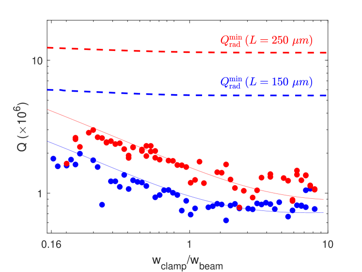
S1(a): Comparison of the measured values and the simulated, radiation-limited . For all data series, the color encodes the device length (blue - , red - ). The dots represent measured data, while the solid lines correspond to the numerical model for a strained beam dominated by intrinsic material losses (reproduced from the main text). The dashed upper lines display : a lower bound on the limit from radiative escape of mechanical energy to the substrate, as calculated with a zero-free-parameters finite element model.
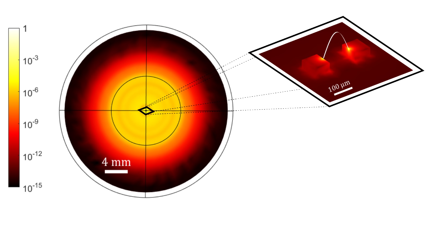
S1(b): Visualization of the far-field (left) and near-field (enlarged view, on the right) radiation pattern for the fundamental OP mode. The color encodes the displacement amplitude in logarithmic scale and normalized units. The strain field leaks from the vibrating beam to the support pillars and to the silicon substrate, displaying a much larger acoustic wavelength. In the left image, the overlaid contours show the profile of the beam (in the center), the boundary between substrate and PML (inner circle) and the outer boundary of the model (outer circle). The displacement amplitude decays exponentially after crossing the PML boundary. The framed image on the right shows the near-field displacement profile in the vicinity of the nanobeam, on a scale much smaller than the acoustic wavelength in the substrate.
II Effect of beam width on the factor
In order to investigate radiation losses experimentally, we fabricated a set of beams with varying but the same clamp-to-beam ratio. Previous studies of nanobeams suggest that reducing the beam width can decrease the coupling of the resonator to the substrate via the anchor points Schmid et al. (2011). Therefore, we would expect to see if radiation losses are the dominant source of loss. We therefore characterize devices with a fixed clamp to beam width ratio (), taper slope () and taper transition length (), but reduced beam width compared to the devices used in Fig. 4 of the main text.
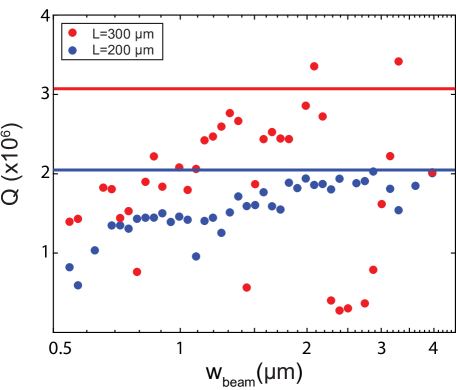
The data presented in S2 shows that narrower , corresponding to lower coupling of the resonator to the substrate, does not enhance the . Rather, we see the opposite trend: the decreases for lower widths. We suspect this is due to fabrication imperfections, as the required feature size becomes smaller for narrower beams. Past studies have shown that the intrinsic quality factor of is limited by surface losses. The sidewalls of the beam have considerably lower surface quality than the top and bottom, due to the nature of the dry etch process used for the beam pattern definition. The observed width dependence could therefore be due to loss contributions from the sidewall surfaces, which for our thickness constitute one fifth of the surface area for the narrowest beams measured. The observed dependence of on provides further evidence that radiation losses are negligible for our samples.
III Breaking stress of
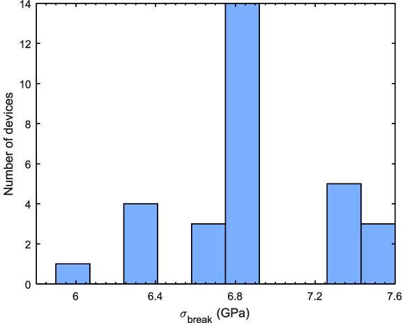
In order to estimate the breaking stress of , we investigate the breaking point of nanobeams of different lengths as we sweep the clamp to beam width ratio. On each chip we sweep the clamp-to-beam width ratio () from 10 to 0.05 with 80 devices. This sweep is repeated for three different beam lengths of , and . By observing the devices under the microscope, we determine the breaking point of our nanobeam devices and infer the yield stress of LPCVD . The deposition stress of our film is known to be 1.14 GPa in previous studiesGhadimi et al. (2018).
We observe that the most likely yield stress of our film is 6.8 GPa, corresponding to . Maximum and minimum yield stress observed were respectively 7.6 GPa and 6 GPa corresponding to and . The spread of the measured yield stress of data is plotted in Fig. S3.
IV Transverse buckling of film
We observe buckling in the film when reaching high stress ( GPa) in high aspect ratio designs. This effect is caused by the bi-axial relaxation of stress in the transverse direction around the corner points. Compressive stress develops in the transverse direction when the longitudinal stress is increased beyond 2 GPa. We observed this effect in 20-nm thick films when the clamp-to-beam width ratio was below 0.4.
References
- Wilson-Rae et al. (2011) I. Wilson-Rae, R. Barton, S. Verbridge, D. Southworth, B. Ilic, H. Craighead, and J. Parpia, Physical Review Letters 106, 047205 (2011).
- Villanueva and Schmid (2014) L. G. Villanueva and S. Schmid, Physical Review Letters 113, 227201 (2014).
- Tsaturyan et al. (2014) Y. Tsaturyan, A. Barg, A. Simonsen, L. G. Villanueva, S. Schmid, A. Schliesser, and E. S. Polzik, Optics Express 22, 6810 (2014).
- Unterreithmeier et al. (2010) Q. P. Unterreithmeier, T. Faust, and J. P. Kotthaus, Physical Review Letters 105, 027205 (2010).
- Ghadimi et al. (2017) A. H. Ghadimi, D. J. Wilson, and T. J. Kippenberg, Nano letters 17, 3501 (2017).
- Schmid et al. (2011) S. Schmid, K. Jensen, K. Nielsen, and A. Boisen, Physical Review B 84, 165307 (2011).
- Photiadis and Judge (2004) D. M. Photiadis and J. A. Judge, Applied Physics Letters 85, 482 (2004).
- Cross and Lifshitz (2001) M. Cross and R. Lifshitz, Physical Review B 64, 085324 (2001).
- Note (1) A PML is an artificial, anisotropic material with finite absorption, designed to be perfectly impedance-matched with the impinging waves at each point. Its introduction avoids the generation of spurious reflected waves at the interface with the physical support, which would alter the simulated dissipation.
- Ghadimi et al. (2018) A. H. Ghadimi, S. A. Fedorov, N. J. Engelsen, M. J. Bereyhi, R. Schilling, D. J. Wilson, and T. J. Kippenberg, Science 360, 764 (2018).