Carbon Nanotube Millikelvin Transport and Nanomechanics
Abstract
Single wall carbon nanotubes cooled to cryogenic temperatures are outstanding electronic as well as nano-electromechanical model systems. To probe a largely unperturbed system, we measure a suspended carbon-nanotube device where the nanotube is grown in the last fabrication step, thus avoiding damage and residues from subsequent processing. In this ultra-clean device, we observe the transport spectrum and its interaction with nano-electromechanics over a wide gate voltage range and thereby over a wide range of coupling parameters between the quantum dot and the contact electrodes.
I Introduction
Both the electronic and the nano-electromechanical low-temperature properties of single-wall carbon nanotubes have attracted significant research over the past decades, resulting in a large spectrum of publications Laird et al. (2015). In particular “ultraclean”, as grown carbon nanotubes are prototypical single-electron devices Cao et al. (2005), where the unperturbed transport spectrum reveals a wide range of phenomena originating from the band structure Kuemmeth et al. (2008); Steele et al. (2009a); Pei et al. (2012); Schmid et al. (2015a) and the interaction between the charge carriers Deshpande and Bockrath (2008); Hamo et al. (2016); Shapir et al. (2018); Island et al. (2018). At the same time, single-wall carbon nanotubes at millikelvin temperatures are excellent mechanical resonators Sazonova et al. (2004); Witkamp et al. (2006); Hüttel et al. (2009), with resonance frequencies up to Laird et al. (2012) and quality factors up to Moser et al. (2014). In suspended carbon nanotube devices, the electrostatic forces acting on single electrons dominate the mechanical behaviour, and electronic transport is subject to strong coupling between single electron tunneling and vibrational motion Steele et al. (2009b); Hüttel et al. (2010); Lassagne et al. (2009).
Typically, reports focus on selected aspects of the behaviour of carbon nanotubes, possibly across several devices. While this is a suitable approach for in-depth analysis of the observed phenomena, it is challenging to obtain a complete picture of the behaviour of one single wall nanotube device across all regimes of coupling to the leads. Here, we present low-temperature measurement data collected on a single device. We follow both electronic and nano-electromechanical phenomena from the highly transparent transport through hole states, across the band gap to strong Coulomb blockade, and finally towards larger electron numbers, where the tunnel barriers become increasingly transparent with higher order transport processes dominating the current.
The schematic device geometry is sketched in
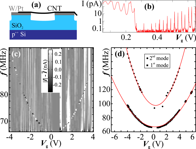
Fig. 1(a). The device fabrication follows the approach of Cao et al. (2005). We start with a highly p++ doped silicon wafer having a 500nm dry-grown thermal surface oxide. The contact electrodes, with a bilayer of 10nm tungsten and 40nm platinum, are fabricated using electron beam lithography, metal evaporation, and lift-off. Subsequently, the silicon oxide surface is anisotropically etched by 100nm to deepen the trenches between the electrodes. Nanotube growth catalyst is locally deposited via an additional lithography step, drop-casting, and lift-off Kong et al. (1998). In the final fabrication step, the carbon nanotubes are grown in situ by chemical vapour deposition Kong et al. (1998). The distance between the contact electrodes is , providing a lower boundary for the length of the active nanotube segment.
A measurement of the low-bias () current through the device at base temperature of the dilution refrigerator is plotted in Fig. 1(b). On the hole conduction side, i.e. for , the device is highly transparent, while the electron conduction side, , initially displays strong Coulomb blockade. This indicates that the actual contacts between nanotube and platinum electrodes are transparent. The opaque tunnel barriers of the quantum dot at low electron number are given by the extended p-n junctions between the electrostatically n-doped central nanotube segment and the nanotube segments close to the leads Park and McEuen (2001); Kuemmeth et al. (2008); Margańska et al. (2017).
Figure 1(c) shows a measurement of the transversal vibrational resonance of the carbon nanotube Sazonova et al. (2004); Witkamp et al. (2006). Here, the detection scheme of Hüttel et al. (2009); Steele et al. (2009b); Schmid et al. (2012) is used: an antenna several millimeters from the device radiatively introduces a MHz signal, and the resulting driven vibration at mechanical resonance leads to a peak or dip in detected dc-current due to the modulated displacement of the nanotube and the resulting modulation in gate capacitance. We observe a strong gate voltage dependence of the resonance frequency due to the changing tension in the nanotube induced by the pull of the gate voltage. The resonance from Fig. 1(c) and an additional second mode at higher frequency are extracted in Fig. 1(d). In both cases, a parabolic fit provides a good (though strongly simplified) approximation of the gate voltage dependence in the measured range (cf. Witkamp et al. (2006); Poot et al. (2007) for a more detailed model).
II Hole transport region
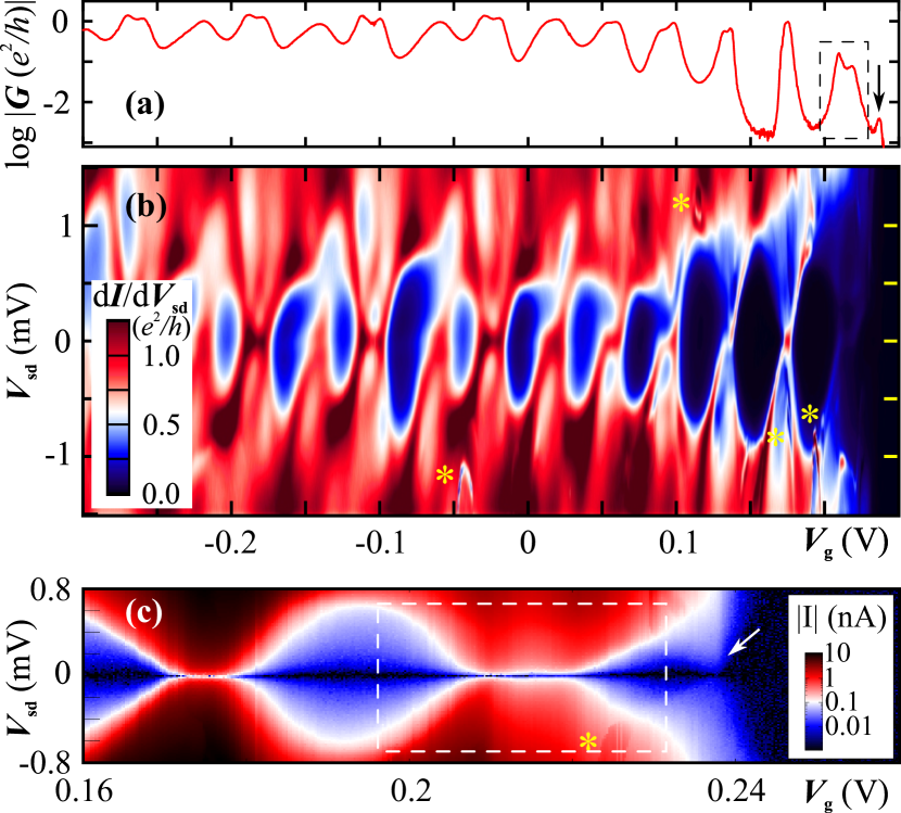
At gate voltages , current is carried by valence band states, and the quantum dot is charged with an increasing number of holes for decreasing gate voltage. Due to the absence of abovementioned p-n barriers, the device displays strong coupling to the metal contacts. This is illustrated in Fig. 2; note that while the line plot of Fig. 2(a) is logarithmic, the color scale of Fig. 2(b) is linear. The pronounced sequence of conductance oscillations at zero bias turns, upon closer observation, out to be a sequence of Kondo conductance ridges Goldhaber-Gordon et al. (1998); Nygård et al. (2000); Jarillo-Herrero et al. (2005); Schmid et al. (2015a) corresponding each to the addition of two holes. This is particluarly obvious around , , , where a clear Kondo zero bias anomaly of conductance emerges. The yellow asterisks in Fig. 2 mark characteristic lobe-shaped features with sharp edges in the data which correspond to mechanical instability and vibrational feedback phenomena in transport Usmani et al. (2007); Steele et al. (2009b); Schmid et al. (2012, 2015b).
Figure 2(c) zooms in on the band gap edge; here we plot the absolute value of the dc current in logarithmic scale since this allows us to resolve smaller signals. The feature at turns out to be a clear double-peak, i.e., two nearly merged Coulomb oscillations, consistent with the curve shape of Fig. 2(a) [see the dashed boxes in both figures]. Since the Kondo ridges are associated with odd electron or hole numbers, this means that at the nanotube is charged with an even number of holes. This leaves us with a conundrum about the nature of the structure at , also visible as a single sharp peak in Fig. 2(a) and marked in both figures with an arrow. Two explanations are possible: either this is a single Coulomb oscillation and an additional oscillation cannot be resolved due to too small tunnel rates, or this peak is already a merger of two oscillations. The former explanation seems unlikely since, even at high bias, no further structures in current or conductance are visible at the hole side of the band gap region. Measurements at larger temperature and at finite magnetic field may provide additional information.
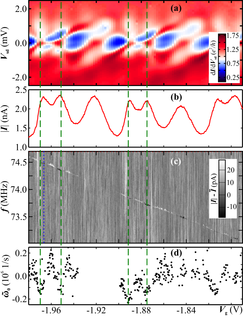
A stability diagram at larger hole number, where the interfaces between the carbon nanotube and its contact electrodes become increasingly transparent towards Fabry-Pérot conduction Liang et al. (2001); Dirnaichner et al. (2016), is plotted in Fig. 3(a). In absence of the (SU(2)) Kondo effect at even electron number, elastic co-tunneling enables large conductance in nominal Coulomb blockade regions De Franceschi et al. (2001). For odd electron numbers, Coulomb blockade is suppressed at low bias, and, as already observed in Fig. 2, several of the conductance peaks merge completely into Kondo ridges. This is also clearly visible in the line plot of Fig. 3(b), displaying the current at .
The subseqent panel, Fig. 3(c), shows the result of mechanical resonance detection in the same gate voltage region, using the same measurement and plotting scheme as Fig. 1(c), though at much lower driving power (nominally ). The fundamental vibration mode becomes clearly visible as a diagonal feature. In the plotted gate voltage region it displays a near-linear dependence on the gate voltage , qualitatively different from the observations of, e.g., Steele et al. (2009b); Meerwaldt et al. (2012); Benyamini et al. (2014); Häkkinen et al. (2015), where each Coulomb oscillation causes a strong dip in frequency due to changing electrostatic forces in response to single charge tunneling at the charge degeneracy points. This indicates that, due to increased tunnel rates and lifetime broadening of the involved quantum levels, Coulomb blockade is gradually lost Götz et al. (2018) and that the nanotube more and more resembles a metallic beam. However, a more detailed analysis (Fig. 3(d)), where the resonance frequency has been extracted and a linear contribution has been removed, still allows to identify some of the characteristic oscillations of , corresponding to the addition of single holes to the system Steele et al. (2009b); Götz et al. (2018); selected features are marked in the figure with vertical dashed lines.
For even larger negative gate voltages, our device unambiguously enters the Fabry-Pérot regime, where weak scattering of the electronic wavefunctions at the contacts causes quantum interference Liang et al. (2001). A detailed discussion of the properties of the device in this parameter region can be found in Dirnaichner et al. (2016).
III Strong Coulomb blockade
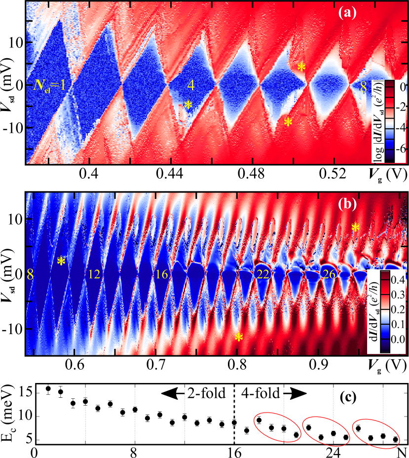
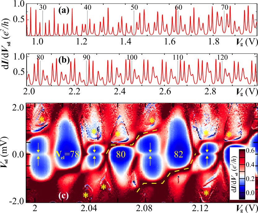
The differential conductance measurements of Fig. 4 cover the parameter region adjacent to the bandgap towards positive gate voltage, where few electrons are trapped in the carbon nanotube. Fig. 4(a) shows the region in logarithmic color scale. The diamond-shaped regions of Coulomb blockade and fixed number of trapped electrons are clearly visible. Additionally, we observe multiple conductance lines in the single electron tunneling regions corresponding to excited quantum states. Already in the Coulomb blockade region with , further lobe-shaped features appear, becoming much stronger at (see the yellow asterisks in the figure). These again correspond to vibrational feedback phenomena typical for clean and suspended carbon nanotube devices at millikelvin temperatures Usmani et al. (2007); Steele et al. (2009b); Schmid et al. (2012, 2015b).
Fig. 4(b) continues the plot of Fig. 4(a) towards larger electron numbers , now in linear color scale. The lobe-shaped instability regions now occur repetitively for every Coulomb oscillation. In addition, near-horizontal features in Coulomb blockade, which can be associated with inelastic cotunneling De Franceschi et al. (2001) and the non-equilibrium Kondo effect Nygård et al. (2000); Gaass et al. (2011); Schmid et al. (2015a), become increasingly prominent.
A plot of the charging energy as function of electron number is provided in Fig. 4(c). It displays the overall decrease of with , typical for this type of device, in addition to ”shell-effects” from subsequent filling of quantum levels analogous to shells in atomic physics. Interestingly, the shell-filling results in a two-fold pattern for , while for a fourfold peak grouping with the largest charging energy at is observed. Electron-electron interaction effects are a likely cause of this phenomenon Deshpande and Bockrath (2008), requiring further analysis and potentially additional measurements in magnetic fields.
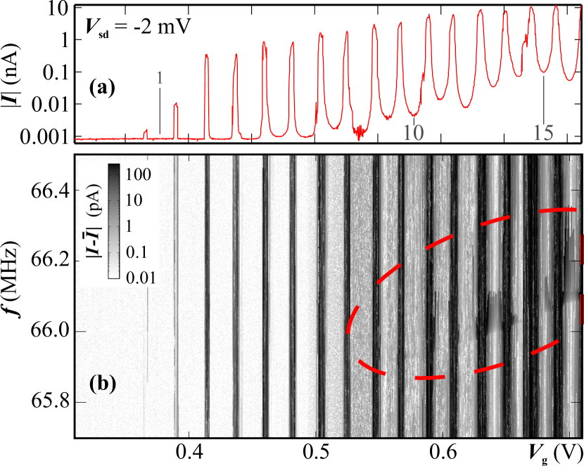
Figure 5 illustrates the attempt to resolve the transversal vibration resonance for decreasing electron numbers all the way to the electronic band gap. Even though a comparatively large bias of (see Fig. 5(a)) is applied, the resonance peaks only remain detectable for , as marked by an ellipsiod in Fig. 5(b). The peaks are far in the nonlinear response regime, displaying an abrupt edge similar to a Duffing oscillator response at increasing driving frequency. For the resonant response becomes too small to be detected. To be able to trace the transversal vibration resonance frequency across the low electron number region, and specifically also the electronic band gap, a different detection scheme is required.
IV Large electron numbers
With increasing positive gate voltage and thereby increasing number of trapped electrons , higher order tunneling processes become dominant in the transport spectrum. This is immediately visible in the differential conductance plots of Figs. 6(a) and (b), where the Kondo effect and (to a lesser degree) elastic cotunneling increase the signal. While the conductance trace retains an overall fourfold repetitive pattern, corresponding to the fourfold occupation of each longitudinal momentum state in the nanotube confinement potential, the precise shape of the conductance oscillations continuously evolves towards Kondo ridges and suppressed Coulomb blockade.
An example stability diagram, plotting the differential conductance as function of gate voltage and bias voltage in the region , is shown in Fig. 6(c). A zero bias conductance anomaly becomes clearly visible at odd electron number, though it is here still comparatively weak. An evaluation of the Kondo ridge width, following Kretinin et al. (2012), leads to typical Kondo temperatures of at the center of the depicted odd- Coulomb blockade regions.
Much more dominant in Fig. 6(c) are, however, different effects. As marked by dashed lines in the figure, strong, discrete conductance resonances at finite bias pass stepwise through the Coulomb blockade regions. Going beyond inelastic cotunneling, which would lead to a conductance threshold alone, these lines again correspond to nonequilibrium Kondo phenomena Nygård et al. (2000); Gaass et al. (2011); Schmid et al. (2015a). Similar “stepwise” resonance structures have been observed before and identified with an imbalance of the two tunnel barriers connecting a quantum dot to its leads Makarovski et al. (2007). Finally, regions of mechanical instability, marked with asterisks in Fig. 6(c), now consistently occur at nearly every electron number for bias values above and strongly distort the transport spectrum.
V Conclusions
While a clean and suspended carbon nanotube may seem like a comparatively simple object, its spectroscopy reveals an immense richness of phenomena in electronics, nanomechanics, and the coupling of both. The tunability of the tunnel couplings via the gate voltage allows access to a wide parameter range, from the electronic band gap and strong Coulomb blockade all the way to higher order tunneling phenomena and eventually Fabry-Pérot interference. In nearly all of these regions nano-electromechanical phenomena can be identified. A driving signal makes it possible to detect the transversal vibration resonance frequency from low electron numbers all the way to the strong Kondo regime; even where charge quantization is nearly lost, a detailed analysis of the resonance frequency evolution still allows to characterize the electronic system via its quantum capacitance. Additionally, nano-electromechanical feedback effects dominate the current at finite bias, leading to strongly distorted transport spectra. The tunability of a single, clean device allows the direct comparison of parameter regimes Niklas et al. (2016), at known electron number and unchanged molecular structure.
Acknowledgments
We would like to thank Ch. Strunk and D. Weiss for the use of experimental facilities. The authors acknowledge funding by the Deutsche Forschungsgemeinschaft via Emmy Noether grant Hu 1808/1, SFB 689, and SFB 1277. The measurement data has been recorded using the Lab::Measurement software package Reinhardt et al. (2019).
References
- Laird et al. (2015) E. A. Laird, F. Kuemmeth, G. A. Steele, K. Grove-Rasmussen, J. Nygård, K. Flensberg, and L. P. Kouwenhoven, “Quantum transport in carbon nanotubes,” Rev. Mod. Phys. 87, 703 (2015).
- Cao et al. (2005) J. Cao, Q. Wang, and H. Dai, “Electron transport in very clean, as-grown suspended carbon nanotubes,” Nature Materials 4, 745 (2005).
- Kuemmeth et al. (2008) F. Kuemmeth, S. Ilani, D. C. Ralph, and P. L. McEuen, “Coupling of spin and orbital motion of electrons in carbon nanotubes,” Nature 452, 448 (2008).
- Steele et al. (2009a) G. A. Steele, G. Gotz, and L. P. Kouwenhoven, “Tunable few-electron double quantum dots and klein tunnelling in ultraclean carbon nanotubes,” Nat. Nanotech. 4, 363 (2009a).
- Pei et al. (2012) F. Pei, E. A. Laird, G. A. Steele, and L. P. Kouwenhoven, “Valley-spin blockade and spin resonance in carbon nanotubes,” Nat. Nanotechn. 7, 630 (2012).
- Schmid et al. (2015a) D. R. Schmid, S. Smirnov, M. Margańska, A. Dirnaichner, P. L. Stiller, M. Grifoni, A. K. Hüttel, and Ch. Strunk, “Broken SU(4) symmetry in a Kondo-correlated carbon nanotube,” Phys. Rev. B 91, 155435 (2015a).
- Deshpande and Bockrath (2008) V. V. Deshpande and M. Bockrath, “The one-dimensional Wigner crystal in carbon nanotubes,” Nature Physics 4, 314 (2008).
- Hamo et al. (2016) A. Hamo, A. Benyamini, I. Shapir, I. Khivrich, J. Waissman, K. Kaasbjerg, Y. Oreg, F. von Oppen, and S. Ilani, “Electron attraction mediated by Coulomb repulsion,” Nature 535, 395 (2016).
- Shapir et al. (2018) I. Shapir, A. Hamo, S. Pecker, C. Pascu Moca, Ö. Legeza, G. Zarand, and S. Ilani, “Imaging the Wigner crystal of electrons in one dimension,” (2018), arXiv:1803.08523.
- Island et al. (2018) J. O. Island, M. Ostermann, L. Aspitarte, E. D. Minot, D. Varsano, E. Molinari, M. Rontani, and G. A. Steele, “Interaction-driven giant orbital magnetic moments in carbon nanotubes,” Phys. Rev. Lett. 121, 127704 (2018).
- Sazonova et al. (2004) V. Sazonova, Y. Yaish, H. Üstünel, D. Roundy, T. A. Arias, and P. L. McEuen, “A tunable carbon nanotube electromechanical oscillator,” Nature 431, 284 (2004).
- Witkamp et al. (2006) B. Witkamp, M. Poot, and H.S.J. van der Zant, “Bending-mode vibration of a suspended nanotube resonator,” Nano Lett. 6, 2904 (2006).
- Hüttel et al. (2009) A. K. Hüttel, G. A. Steele, B. Witkamp, M. Poot, L. P. Kouwenhoven, and H. S. J. van der Zant, “Carbon nanotubes as ultra-high quality factor mechanical resonators,” Nano Letters 9, 2547 (2009).
- Laird et al. (2012) E. A. Laird, F. Pei, W. Tang, G. A. Steele, and L. P. Kouwenhoven, “A high quality factor carbon nanotube mechanical resonator at 39 GHz,” Nano Letters 12, 193 (2012).
- Moser et al. (2014) J. Moser, A. Eichler, J. Güttinger, M. I. Dykman, and A. Bachtold, “Nanotube mechanical resonators with quality factors of up to 5 million,” Nature Nanotechnology 9, 1007 (2014).
- Steele et al. (2009b) G. A. Steele, A. K. Hüttel, B. Witkamp, M. Poot, H. B. Meerwaldt, L. P. Kouwenhoven, and H. S. J. van der Zant, “Strong coupling between single-electron tunneling and nanomechanical motion,” Science 325, 1103 (2009b).
- Hüttel et al. (2010) A. K. Hüttel, H. B. Meerwaldt, G. A. Steele, M. Poot, B. Witkamp, L. P. Kouwenhoven, and H. S. J. van der Zant, “Single electron tunnelling through high-Q single-wall carbon nanotube NEMS resonators,” Phys. Stat. Sol. b 247, 2974 (2010).
- Lassagne et al. (2009) B. Lassagne, Y. Tarakanov, J. Kinaret, D. Garcia-Sanchez, and A. Bachtold, “Coupling mechanics to charge transport in carbon nanotube mechanical resonators,” Science 325, 1107 (2009).
- Kong et al. (1998) J. Kong, H. T. Soh, A. M. Cassell, C. F. Quate, and H. Dai, “Synthesis of individual single-walled carbon nanotubes on patterned silicon wafers,” Nature 395, 878 (1998).
- Park and McEuen (2001) J. Park and P. L. McEuen, “Formation of a p-type quantum dot at the end of an n-type carbon nanotube,” Applied Physics Letters 79, 1363 (2001).
- Margańska et al. (2017) M. Margańska, D. R. Schmid, P. L. Stiller, A. Dirnaichner, Ch. Strunk, M. Grifoni, and A. K. Hüttel, “Shaping electron wave functions in a carbon nanotube with a parallel magnetic field,” (2017), arXiv:1712.08545.
- Schmid et al. (2012) D. R. Schmid, P. L. Stiller, Ch. Strunk, and A. K. Hüttel, “Magnetic damping of a carbon nanotube nano-electromechanical resonator,” New Journal of Physics 14, 083024 (2012).
- Poot et al. (2007) M. Poot, B. Witkamp, M. A. Otte, and H. S. J. van der Zant, “Modelling suspended carbon nanotube resonators,” Phys. Stat. Sol. b 244, 4252 (2007).
- Goldhaber-Gordon et al. (1998) D. Goldhaber-Gordon, Hadas Shtrikman, D. Mahalu, David Abusch-Magder, U. Meirav, and M. A. Kastner, “Kondo effect in a single-electron transistor,” Nature 391, 156 (1998).
- Nygård et al. (2000) J. Nygård, H. C. Cobden, and P. E. Lindelof, “Kondo physics in carbon nanotubes,” Nature 408, 342 (2000).
- Jarillo-Herrero et al. (2005) P. Jarillo-Herrero, J. Kong, H. S. J. van der Zant, C. Dekker, L. P. Kouwenhoven, and S. De Franceschi, “Orbital Kondo effect in carbon nanotubes,” Nature 434, 484 (2005).
- Usmani et al. (2007) O. Usmani, Ya. M. Blanter, and Y. V. Nazarov, “Strong feedback and current noise in nanoelectromechanical systems,” Phys. Rev. B 75, 195312 (2007).
- Schmid et al. (2015b) D. R. Schmid, P. L. Stiller, Ch. Strunk, and A. K. Hüttel, “Liquid-induced damping of mechanical feedback effects in single electron tunneling through a suspended carbon nanotube,” Appl. Phys. Lett. 107, 123110 (2015b).
- Götz et al. (2018) K. J. G. Götz, D. R. Schmid, F. J. Schupp, P. L. Stiller, Ch. Strunk, and A. K. Hüttel, “Nanomechanical characterization of the Kondo charge dynamics in a carbon nanotube,” Phys. Rev. Lett. 120, 246802 (2018).
- Meerwaldt et al. (2012) H. B. Meerwaldt, G. Labadze, B. H. Schneider, A. Taspinar, Y. M. Blanter, H. S. J. van der Zant, and G. A. Steele, “Probing the charge of a quantum dot with a nanomechanical resonator,” Phys. Rev. B 86, 115454 (2012).
- Liang et al. (2001) W. Liang, M. Bockrath, D. Bozovic, J. H. Hafner, M. Tinkham, and H. Park, “Fabry-Pérot interference in a nanotube electron waveguide,” Nature 411, 665 (2001).
- Dirnaichner et al. (2016) A. Dirnaichner, M. del Valle, K. J. G. Götz, F. J. Schupp, N. Paradiso, M. Grifoni, Ch. Strunk, and A. K. Hüttel, “Secondary electron interference from trigonal warping in clean carbon nanotubes,” Phys. Rev. Lett. 117, 166804 (2016).
- De Franceschi et al. (2001) S. De Franceschi, S. Sasaki, J. M. Elzerman, W. G. van der Wiel, S. Tarucha, and L. P. Kouwenhoven, “Electron cotunneling in a semiconductor quantum dot,” Phys. Rev. Lett. 86, 878 (2001).
- Benyamini et al. (2014) A. Benyamini, A. Hamo, S. V. Kusminskiy, F. von Oppen, and S. Ilani, “Real-space tailoring of the electron-phonon coupling in ultraclean nanotube mechanical resonators,” Nat. Phys. 10, 151 (2014).
- Häkkinen et al. (2015) P. Häkkinen, A. Isacsson, A. Savin, J. Sulkko, and P. Hakonen, “Charge sensitivity enhancement via mechanical oscillation in suspended carbon nanotube devices,” Nano Letters 15, 1667 (2015).
- Gaass et al. (2011) M. Gaass, A. K. Hüttel, K. Kang, I. Weymann, J. von Delft, and Ch. Strunk, “Universality of the Kondo effect in quantum dots with ferromagnetic leads,” Phys. Rev. Lett. 107, 176808 (2011).
- Kretinin et al. (2012) A. V. Kretinin, H. Shtrikman, and D. Mahalu, “Universal line shape of the Kondo zero-bias anomaly in a quantum dot,” Phys. Rev. B 85, 201301 (2012).
- Makarovski et al. (2007) A. Makarovski, J. Liu, and G. Finkelstein, “Evolution of transport regimes in carbon nanotube quantum dots,” Phys. Rev. Lett. 99, 066801 (2007).
- Niklas et al. (2016) M. Niklas, S. Smirnov, D. Mantelli, M. Marganska, N.-V. Nguyen, W. Wernsdorfer, J.-P. Cleuziou, and M. Grifoni, “Blocking transport resonances via Kondo many-body entanglement in quantum dots,” Nat. Commun. 7, 12442 (2016).
- Reinhardt et al. (2019) S. Reinhardt, C. Butschkow, S. Geissler, A. Dirnaichner, F. Olbrich, C. Lane, D. Schröer, and A. K. Hüttel, “Lab::Measurement — a portable and extensible framework for controlling lab equipment and conducting measurements,” Computer Physics Communications 234, 216 (2019).