Current address: ]imec, Kapeldreef 75, 3001 Leuven, Belgium
Thermal resistance of GaN/AlN graded interfaces
Abstract
Compositionally graded interfaces in power electronic devices eliminate dislocations, but they can also decrease thermal conduction, leading to overheating. We quantify the thermal resistances of GaN/AlN graded interfaces of varying thickness using ab initio Green’s functions, and compare them with the abrupt interface case. A non-trivial power dependence of the thermal resistance versus interface thickness emerges from the interplay of alloy and mismatch scattering mechanisms. We show that the overall behavior of such graded interfaces is very similar to that of a thin-film of an effective alloy in the length scales relevant to real interfaces.
I Introduction
The common strategy of interfacing two pure semiconductors via a gradual alloyed region poses a design trade-off: on the one hand, a thicker alloyed region is desirable in order to accommodate the lattice mismatch; on the other hand, a thick alloy will also negatively impact the thermal conductance across the interface, possibly degrading a device’s lifetime. For example, common substrate designs for High Electron Mobility Transistors (HEMTs) include a graded transition region between GaN and AlN as thick as 111C. Giesen, private communication. For substrates grown on Si, this region contributes only 3% of the total substrate thermal resistance. But if one replaces Si by diamond, the graded interface thermal resistance amounts to 20% of the total. For common operating conditions in HEMTs this translates into a higher temperature of the active region, shortening the device’s lifetime by one half 222Assuming of Si or diamond, and for the graded region.
Thus, it may pay off to try to make the graded region as thin as possible while still satisfying some minimum structural constraints. To do this one needs to know how the interface thermal resistance depends on its thickness and composition profile. Theoretically quantifying it is, however, a nontrivial problem due to the simultaneous emergence of quasiballistic transport, wave interference effects, and the interplay between large-scale features and atomic-scale disorder. All this leads to a thermal resistance that no longer depends linearly on thickness when the latter gets below the range. Experimentally one can only access the thermal conduction of the structure as a whole, which typically includes many different material interfaces in a single sample. This makes it difficult to quantify the upper limits to interface conductance based on experiments alone. It is therefore very important to theoretically predict the thermal conductance of graded interfaces, to know how much the grading strategy is degrading the performance of devices, and how much improvement could be achieved by other schemes, like reducing thickness or using digital structures. We tackle this question here for the technologically important case of GaN/AlN interfaces, which are ubiquitous in power electronics where thermal dissipation issues are a major concern.
The use of graded interfaces to reduce threading dislocation density was theoretically tackled by Tersoff using an analytical model, and has been deeply explored in subsequent modeling studies for two decades Tersoff (1993); Bertoli et al. (2009). The specific grading length and profile to satisfy structural constraints (e.g. dislocation density or strain) depends on the particular problem in hand. The structural constraint aspect is not the goal of this paper, and we refer the reader to earlier literature.
To model the thermal conductance of interfaces, mainstream techniques include the use of different phonon-gas models such as the diffuse mismatch or acoustic mismatch models, atomistic Green’s functions, or molecular dynamicsSwartz and Pohl (1989); Liang et al. (2014); Gaskins et al. (2018); Ong (2018). A few theoretical studies have focused on trying to improve the interface thermal conductance between two different materials by using mass gradientsZhou et al. (2016). However, in practice, the intermediate layers are often not perfectly ordered in the plane perpendicular to the interface, but rather disordered alloys at a given composition. This is the case that we study here, using Monte Carlo simulations to account for the anharmonic and alloy scattering effects coupled to atomistic Green’s functions to compute the probability of transmission at the interface of two materials. We focus on the case of a very progressive step graded interface and show that the total interface can be modeled as a thin film of an effective alloy, due to the dominant contribution from alloy scattering at realistic length scales. According to recent experimental results Gaskins et al. (2018), the interface thermal resistance can actually be overestimated by atomistic Green’s functions due to additional conductance from non-elastic processes, so this statement should be very robust in the case of those progressive interfaces of two similar crystal structures. We give a general expression for the characteristics of this effective alloy, such that the result can be easily applied to other interfaces profiles.
II Methods
Current approaches to investigate interface thermal conductance atomistically are based on Green’s functions Mingo and Yang (2003); Mingo (2009); Ong and Zhang (2015); Tian et al. (2014); Wang et al. (2008); Zhang et al. (2007, 2010). However, when the interface is structurally complex or disordered in an extended region of space, like in the case of graded interfaces, it is impractical to simulate the whole atomically disordered interface. Doing so would require approximating the disordered interface by multiple realizations of exceedingly large supercells, periodic in the directions parallel to the interface Tian et al. (2014). A method to overcome this limitation was demonstrated in Refs. Chen et al., 2013; Carrete et al., 2018. The basic idea is that the perturbation part of the Hamiltonian can be written as the sum of a contribution from the average perturbation over the layer (the “compositional profile” contribution), plus the local deviation with respect to this average for each atom (the “disorder” contribution). The total phonon scattering intensity is the sum of the scattering intensities of each of the two contributions separately, plus the interference term between them, which is neglected on the grounds of phase cancellation due to disorder. The “compositional profile” scattering term preserves the phonon quasimomentum component parallel to the interface, and can be efficiently calculated using atomistic Green’s functions. The “disorder” term does not preserve quasimomentum, and it is computed within the framework of the virtual crystal approximation. Using realistic compositional profiles and ab initio calculated force constants, a good agreement with experiment was obtained for superlattices with periods comprising up to atomic layers, without using any adjustable parameters Chen et al. (2013); Carrete et al. (2018).
The approach implemented for superlattices is not directly applicable to single interfaces, and requires modification. The difference comes from the periodic character of the superlattices, versus the local and asymmetric character of the single interface. The repeated structure of the superlattices justifies a picture where phonons travel in an effective medium and are incoherently scattered by the homogeneously distributed changes in composition. The T-matrix formalism is best suited to this problem. In contrast, the materials at each side of the single interface are dissimilar, and thus cannot be be treated by the T-matrix formulation of Refs. Chen et al. (2013); Mingo et al. (2014); Protik et al. (2016), which requires having the same material infinitely far from the interface on either side. Instead, the Green’s function formalism for transmission and reflection probabilities is used here Mingo and Yang (2003); Mingo (2009).
In the considered geometry, the interface is bidimensional and infinite in two directions, so that a transmission or a reflection event will conserve the component of momentum parallel to the interface as well as the energy. The dynamical matrix of each bulk material, calculated ab initio, is first Fourier-transformed in the direction perpendicular to the interface to obtain a set of mixed-space force constants:
| (1) |
where is the chosen number of samples over the Brillouin zone in the direction perpendicular to the interface, and the indexes over atoms, and over Cartesian directions, the dynamical matrix and the masses of the atomic species. are lattice vectors perpendicular to the interface and corresponds to the interactions between layers separated by in real space for a given parallel wavevector.
Using this set of force constants, the 2-D Green’s function of each material is computed using the decimation technique Guinea et al. (1983); Sancho et al. (1985). The interactions between layers of different materials 1 and 2 in real space are obtained from the averaged mixed-space force constants and using the masses of the two different materials. For , the acoustic sum rule is enforced by correcting the values of the diagonal elements. Finally, we obtain the transmission between the two materials using the two-region formulaMingo (2009); Mingo and Yang (2003), for each parallel wavevector:
| (2) |
With , , and the spectral density of states of the decoupled system.
This transmission is subsequently used within the Monte Carlo solver implemented in almaBTE Carrete et al. (2017). The ab initio data for GaN and AlN has been computed in a 5x5x5 supercell within the Local Density Approximation of Density Functional Theory, and can be retrieved from the database of the almaBTE website. For each incoming mode, only outgoing modes which conserve the parallel wavevector and the frequency are considered (for transmission or reflection). When several outgoing modes are available for one incoming mode, their probability is weighted by their group velocity projected on the normal to the interface.
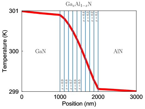
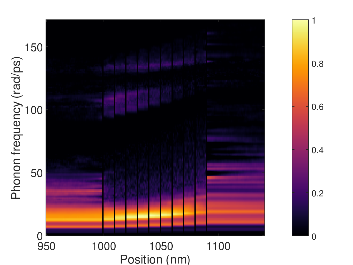
One difficulty in simulating a step graded interface is to combine this mismatch scattering with the intrinsic scattering from the alloy disorder within the layers. To tackle this issue, we choose to slice the interface into steps with gradual increases in composition of 10% (see Fig. 1). In the limit of very short interfaces, mismatch scattering becomes dominant, while if the interface is very thick, alloy scattering takes over.
Finally, the interface thermal resistance is evaluated from the temperature profiles and heat fluxes obtained from the Monte Carlo simulation using buffer layers of at each side of the interface, as:
| (3) |
with representing the total heat flux across the structure and the jump in temperature across the interface.
III Thermal resistances of GaN/AlN step graded interfaces
In the following, we focus on step graded interfaces from GaN to AlN, oriented along the (001) direction. All properties are computed ab initio, using a grid for the phonon wavevectors and samples for the mixed-space force constants.
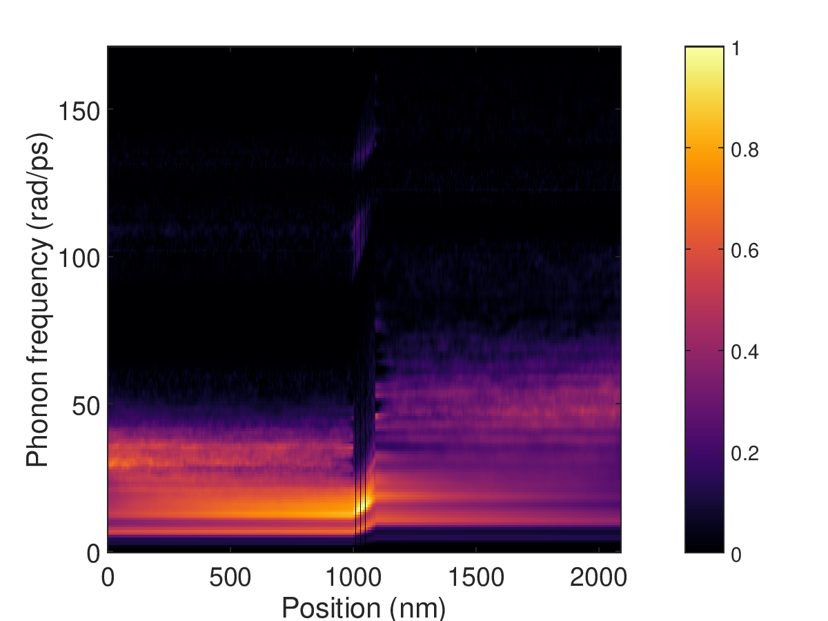
In Figure 1, we display the temperature profile obtained for a step graded interface of about one micron. As can be seen from the absence of temperature jumps, the effect of the successive interfaces on the thermal resistance is negligible compared to the scattering from alloy disorder. In this context, one can model the step graded structure as an effective alloy in which the mass disorder scattering contribution is similar to that of an alloy with concentration GaAlN such that
| (4) |
where the concentration in each layer of the alloy. A similar approach has been shown to give excellent results in the context of superlattices Carrete et al. (2018). Here, and in the continuous limit . At the same time, the phonon spectrum, average masses and three-phonon properties of this effective alloy correspond to those of the average alloy (here with concentration Ga0.5Al0.5N). Finally, the finite length of the interface limits the mean-free path of the phonons, as described in Ref. Vermeersch et al., 2016:
| (5) |
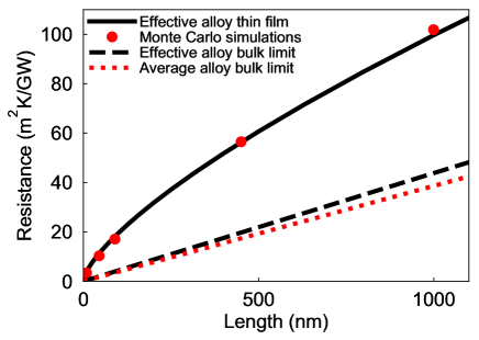
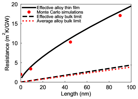
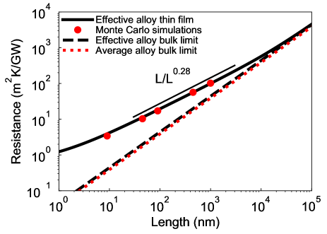
With the thermal resistance of the interface of length , the specific heat of a phonon mode, and its group velocity and mean free path projected on the normal to the interface. As shown in Figure 2, such an approximation gives excellent results in the range of lengths applicable to real interfaces, from nanometer to micrometer scales. We also observe in the lower panel a power law similar to the one found for AlGaN alloys thin films Vermeersch et al. (2016).
In the limit of an infinitely long interface, the resistance should follow an asymptotic trend equal to the total length divided by the average of the bulk conductivities of the different alloys, here compared to the bulk conductivity of the effective alloy of . In the limit of an infinitely thin interface, the conductivity becomes limited by the transmission probability and the resistance of an abrupt interface is computed to be . In contrast, a step graded interface of 9 nm already has a resistance of , showing that the alloy scattering will start to dominate for longer interfaces. Interestingly, this latter value is very much in line with the resistance of the effective alloy (see middle panel of Figure 2). Indeed, at these small length scales the resistance originating from mismatch scattering is partially compensated by a lowering of the resistance caused by alloy scattering, due to the simultaneous filtering of phonon modes at the successive interfaces.
This effect is illustrated by Figure 3, which displays the energy-resolved spectral heat flux of a structure including a GaN/AlN (001) step graded interface of . The successive interfaces are very transparent to the main conduction channels at low energies, while the alloy scattering strongly limits the mean free path of the optical modes around compared to the pure materials. The high-frequency features above are due to the redistribution of phonon population, since their mean-free path is barely impacted by alloy scattering compared to the aforementioned modes around 50 rad/ps. This is due to the different character of those modes: the alloy scattering rates computed within the Tamura formulaTamura (1984) are linked to the density of states of Ga/Al character while the highest modes are mostly of N character, as pointed out in the case of InN by Polanco and Lindsay Polanco and Lindsay (2018). In the framework of the Monte Carlo solver within the Random Time Approximation, the flux is thus redistributed proportionally more in those modes in the alloys than in the pure compounds.
IV Optimizing thermal conductance in real devices
We now discuss the potential optimization of such interfaces. On the one hand, making the graded interface thicker lowers the density of threading dislocations. This improves overall performance in a device-dependent fashion that can be complex to quantify. On the other hand, thicker interfaces can also reduce performance because of device heating resulting from an increased thermal resistance. The balance between these counteracting effects will lead to an optimal grading thickness, which should be optimized on a case-by-case basis for each device. Some current devices are grown on silicon substrate that can be , which adds a thermal resistance of . In such cases the device thermal resistance is dominated by the substrate, making it advantageous to have thick graded regions, since the gain in electrical performance by reducing dislocations is greater than the thermal penalty they contribute.
The picture is very different, however, if a good thermally conducting substrate is employed. For example, diamond’s thermal conductivity is 17 times higher than silicon’s, translating into a thermal resistance for thickness. As Figure 2 shows, in this case the resistance contributed by the graded interfaces in the device would already be a non-negligible part of the total. A difficulty in making good conducting substrates is related to the thermal resistance of the bonding between the substrate and the device. However, very low thermal resistances have recently been achieved for diamond/GaN and SiC/GaN, of and respectively Cho et al. (2012, 2013); Radway (2017). On such new-generation substrates it can pay off to reduce the thickness of the graded regions to some extent, at the expense of an increased dislocation density, to decrease overheating and enhance efficiency and device lifetime.
An increased dislocation density can also lead to increased thermal resistance. However, ab initio calculations and analysis of experimental data indicate that, for dislocation densities under the thermal conductivity reduction in GaN due to dislocations is minimal, and has been overshadowed by thin film effects in previous experiments Wang et al. (2018). The threading dislocation density in GaN directly grown on sapphire, SiC, or Si (111) is typically between Ashby et al. (2000).
The mean-time-to-failure (MTF) of a device is affected by different mechanisms, and its temperature dependence depends on the particular device in hand Burnham et al. (2017); Cheney et al. (2012); Sun et al. (2015); Coffie et al. (2007). Common temperature dependences of GaN device MTFs follow exponential behaviors, and may decrease by one order of magnitude for every 50 °C increase in the temperature of the active region. The operation temperature of High Electron Mobility Transistors can reach well above one hundred degrees Celsius. In the well-bonded diamond substrate case above, the over 20% thermal resistance contributed by a -thick graded interface may thus lead to overheating by and shorten the device’s MTF by half.
V Conclusion
In conclusion, using an ab initio Green’s function approach we have computed the lattice thermal resistances of a series of GaN/AlN (001) step graded interfaces of different lengths. We find that mismatch scattering is very weak in the main conduction channels, such that alloy scattering becomes dominant in the regime relevant for real interfaces ( to ). The computed resistance of the step graded interface is well approximated by that of a model thin-film of an effective alloy, and it strongly deviates from the classical Fourier law predictions. The resistance of and thick interfaces exceeds conventional estimates by twofold and fourfold respectively. In the case of well-sinked devices, graded interfaces add a non-negligible contribution to overheating, and it can be advisable to shorten the thickness of the step graded interfaces at the expense of a larger density of threading dislocations. The thermal resistances calculated in this article represent a valuable information for the optimization of GaN-based power electronic devices.
Acknowledgements.
We acknowledge support from the European Union’s Horizon 2020 Research and Innovation Programme, grant number 645776 (ALMA). We thank C. Giesen for sharing thickness data from real substrates.References
- Note (1) C. Giesen, private communication.
- Note (2) Assuming of Si or diamond, and for the graded region.
- Tersoff (1993) J. Tersoff, Applied Physics Letters 62, 693 (1993).
- Bertoli et al. (2009) B. Bertoli, E. N. Suarez, J. E. Ayers, and F. C. Jain, Journal of Applied Physics 106, 073519 (2009).
- Swartz and Pohl (1989) E. T. Swartz and R. O. Pohl, Rev. Mod. Phys. 61, 605 (1989).
- Liang et al. (2014) Z. Liang, K. Sasikumar, and P. Keblinski, Phys. Rev. Lett. 113, 065901 (2014).
- Gaskins et al. (2018) J. T. Gaskins, G. Kotsonis, A. Giri, S. Ju, A. Rohskopf, Y. Wang, T. Bai, E. Sachet, C. T. Shelton, Z. Liu, Z. Cheng, B. M. Foley, S. Graham, T. Luo, A. Henry, M. S. Goorsky, J. Shiomi, J.-P. Maria, and P. E. Hopkins, Nano Letters 18, 7469 (2018).
- Ong (2018) Z.-Y. Ong, Journal of Applied Physics 124, 151101 (2018).
- Zhou et al. (2016) Y. Zhou, X. Zhang, and M. Hu, Nanoscale 8, 1994 (2016).
- Mingo and Yang (2003) N. Mingo and L. Yang, Physical Review B 68, 245406 (2003).
- Mingo (2009) N. Mingo, Thermal Nanosystems and Nanomaterials , 63 (2009).
- Ong and Zhang (2015) Z.-Y. Ong and G. Zhang, Physical Review B 91, 174302 (2015).
- Tian et al. (2014) Z. Tian, K. Esfarjani, and G. Chen, Physical Review B 89, 235307 (2014).
- Wang et al. (2008) J.-S. Wang, J. Wang, and J. T. Lü, The European Physical Journal B 62, 381 (2008).
- Zhang et al. (2007) W. Zhang, N. Mingo, and T. S. Fisher, Physical Review B 76, 195429 (2007).
- Zhang et al. (2010) W. Zhang, T. S. Fisher, and N. Mingo, Numerical Heat Transfer, Part B: Fundamentals (2010), 10.1080/10407790601144755.
- Chen et al. (2013) P. Chen, N. A. Katcho, J. P. Feser, W. Li, M. Glaser, O. G. Schmidt, D. G. Cahill, N. Mingo, and A. Rastelli, Physical Review Letters 111, 115901 (2013).
- Carrete et al. (2018) J. Carrete, B. Vermeersch, L. Thumfart, R. R. Kakodkar, G. Trevisi, P. Frigeri, L. Seravalli, J. P. Feser, A. Rastelli, and N. Mingo, The Journal of Physical Chemistry C 122, 4054 (2018).
- Mingo et al. (2014) N. Mingo, D. A. Stewart, D. A. Broido, L. Lindsay, and W. Li, in Length-Scale Dependent Phonon Interactions, Topics in Applied Physics No. 128, edited by S. L. Shindé and G. P. Srivastava (Springer New York, 2014) pp. 137–173.
- Protik et al. (2016) N. H. Protik, J. Carrete, N. A. Katcho, N. Mingo, and D. Broido, Physical Review B 94, 045207 (2016).
- Guinea et al. (1983) F. Guinea, C. Tejedor, F. Flores, and E. Louis, Physical Review B 28, 4397 (1983).
- Sancho et al. (1985) M. P. L. Sancho, J. M. L. Sancho, J. M. L. Sancho, and J. Rubio, Journal of Physics F: Metal Physics 15, 851 (1985).
- Carrete et al. (2017) J. Carrete, B. Vermeersch, A. Katre, A. van Roekeghem, T. Wang, G. K. H. Madsen, and N. Mingo, Computer Physics Communications 220, 351 (2017).
- Vermeersch et al. (2016) B. Vermeersch, J. Carrete, and N. Mingo, Applied Physics Letters 108, 193104 (2016).
- Tamura (1984) S.-i. Tamura, Phys. Rev. B 30, 849 (1984).
- Polanco and Lindsay (2018) C. A. Polanco and L. Lindsay, Phys. Rev. B 98, 014306 (2018).
- Cho et al. (2012) J. Cho, E. Bozorg-Grayeli, D. Altman, M. Asheghi, and K. E. Goodson, IEEE Electron Device Letters 33, 378 (2012).
- Cho et al. (2013) J. Cho, Z. Li, E. Bozorg-Grayeli, T. Kodama, D. Francis, F. Ejeckam, F. Faili, M. Asheghi, and K. Goodson, IEEE Transactions on Components, Packaging and Manufacturing Technology 3, 79 (2013).
- Radway (2017) R. M. Radway, PhD thesis, Massachusetts Institute of Technology (2017).
- Wang et al. (2018) T. Wang, J. Carrete, N. Mingo, , and G. K. H. Madsen, unpublished (2018).
- Ashby et al. (2000) C. I. H. Ashby, C. C. Mitchell, J. Han, N. A. Missert, P. P. Provencio, D. M. Follstaedt, G. M. Peake, and L. Griego, Applied Physics Letters 77, 3233 (2000).
- Burnham et al. (2017) S. D. Burnham, R. Bowen, J. Tai, D. Brown, R. Grabar, D. Santos, J. Magadia, I. Khalaf, and M. Micovic, IEEE Transactions on Semiconductor Manufacturing 30, 480 (2017).
- Cheney et al. (2012) D. Cheney, E. Douglas, L. Liu, C.-F. Lo, B. Gila, F. Ren, S. Pearton, D. J. Cheney, E. A. Douglas, L. Liu, C.-F. Lo, B. P. Gila, F. Ren, and S. J. Pearton, Materials 5, 2498 (2012).
- Sun et al. (2015) H. Sun, M. M. Bajo, M. J. Uren, and M. Kuball, Applied Physics Letters 106, 043505 (2015).
- Coffie et al. (2007) R. Coffie, Y. Chen, I. P. Smorchkova, B. Heying, V. Gambin, W. Sutton, Y. Chou, W. Luo, M. Wojtowicz, and A. Oki, in 2007 IEEE International Reliability Physics Symposium Proceedings. 45th Annual (2007) pp. 568–569.