‡ Present Address: Dipartimento di Fisica, Università di Genova, Via Dodecaneso 33, 16146 Genova, Italy
Bimodal Phase Diagram of the Superfluid Density in \ceLaAlO3 / SrTiO3
Revealed by an Interfacial Waveguide Resonator
Abstract
We explore the superconducting phase diagram of the two-dimensional electron system at the \ceLaAlO3 / SrTiO3 interface by monitoring the frequencies of the cavity modes of a coplanar waveguide resonator fabricated in the interface itself. We determine the phase diagram of the superconducting transition as a function of the temperature and electrostatic gating, finding that both the superfluid density and the transition temperature follow a dome shape but that the two are not monotonically related. The ground state of this two-dimensional electron system is interpreted as a Josephson junction array, where a transition from long- to short-range order occurs as a function of the electronic doping. The synergy between correlated oxides and superconducting circuits is revealed to be a promising route to investigate these exotic compounds, complementary to standard magnetotransport measurements.
The interface between the two wide band-gap insulators \ceLaAlO3 (LAO) and \ceSrTiO3 (STO) hosts a two-dimensional electron system (2DES) Ohtomo and Hwang (2004); Cen et al. (2009) that shows superconductivity Reyren et al. (2007) together with strong spin-orbit coupling Ben Shalom et al. (2010); Diez et al. (2015), localized magnetic moments Bert et al. (2011); Li et al. (2011), and long-range spin coherence Ohshima et al. (2017). Its low carrier concentration makes this 2DES particularly sensitive to elecrostatic gating, and a superconductor-insulator transition, tunable Rashba splitting, and tunable superconductivity have already been demonstrated Caviglia et al. (2008); Bell et al. (2009); Caviglia et al. (2010). Despite being considered the prototypical correlated 2DES and a platform to realize tunable superconducting devices Monteiro et al. (2017); Goswami et al. (2016); Thierschmann et al. (2018), the nature of its superconducting ground state and dome-shaped phase diagram, observed upon electrostatic doping, is still not understood. This partly stems from the fact that standard magnetotransport measurements do not allow us to directly probe the superfluid density, and so far few approaches have been proposed to overcome such limitation. Bert et al. employed a scanning-SQUID technique to measure the penetration depth of the screening supercurrents and extract the superfluid density of the 2DES Bert et al. (2012), while, more recently, Singh et al. calculated the variations of the superfluid density from the resonance frequency of a RLC circuit containing a lumped LAO/STO element by means of an equivalent-circuit model Singh et al. (2018). A powerful tool to probe the superfluid density are the superconducting coplanar waveguide resonators (SCWRs). SCWRs are cavities for the electromagnetic field where the frequencies of the standing waves are determined by the interplay between the geometry and electromagnetic environment Lancaster et al. (1998); Tiggelman et al. (2009); Ahmed et al. (2015). The formation of quasiparticles in a SCWR causes a downshift of their resonance frequencies because the lower superfluid density increases the kinetic inductance Baselmans et al. (2007); Vercruyssen et al. (2011). The high sensitivity of such devices warranted their integration in highly demanding applications, such as quantum technologies Nataf and Ciuti (2011); Xiang et al. (2013); Chow et al. (2014) and astronomy Baselmans et al. (2008); Bueno et al. (2017).
Here, we realize a SCWR by direct patterning of the 2DES at the LAO/STO interface. This approach gives a stronger modulation of the resonance frequency in comparison to lumped-element designs used in previous implementations. The resonance frequencies of the SCWR cavity modes are monitored as a function of the temperature and electrostatic doping and translated into variations of the Pearl length and superfluid density. We find that both the critical temperature and superfluid density display a domelike shape as a function of the back-gate voltage, which are not monotonically related. This nonmonotonic behavior arises from the ground state of the system, which is identified as a Josephson junction array shifting from short- to long-range order while driving the system from the under- to overdoped condition.
The pristine heterostructure is obtained by the pulsed laser deposition of 12 unit cells of crystalline LAO on top of a \ceTiO2-terminated \ceSrTiO3(100) substrate. As sketched in Fig. 1(a), by means of electron beam lithography and ion milling, we separate the central line from the ground plane (GND). The line has a width of 40 µm, a nominal length of 2.5 mm, and a spacing of 10 µm from the GND. Details of the fabrication are reported in the Supplemental Material, Sec. 1. One end of the SCWR is isolated from the GND while the other is wire bonded to the feed line. The large impedance mismatch at the two ends of the line realizes a nearly half-wavelength () resonator. The cavity modes of the SCWR are measured with a vector network analyzer (VNA), as indicated in Fig. 1(b). The power of the signal injected into the SCWR is about dBm. The sample is glued to an isolated holder with conductive silver paint, which enables field effect measurements in the back-gate geometry. The GND and the line share the same electrical ground, so the back-gate voltage () affects both. Figure 1(c) shows the response spectrum of the SCWR at mK and V. More than ten modes can be identified on top of an oscillating background, which stems from interference in the connecting circuitry. We based our analysis on the modes from to , because is at the edge of the cutoff frequency of the amplifier (30 MHz) (cf. Fig. 1(b)), and the higher modes show lower visibility in the explored space of parameters. The mode visibility as a function of the temperature and is determined by the proximity to the critical coupling condition and by the damping coming from different sources of losses, with coupling, quasiparticles and dielectric losses being the major ones. Here, the broadening and weakening of the peaks at higher frequencies are in agreement with what is expected from the \ceSrTiO3 substrate Davidovikj et al. (2017).
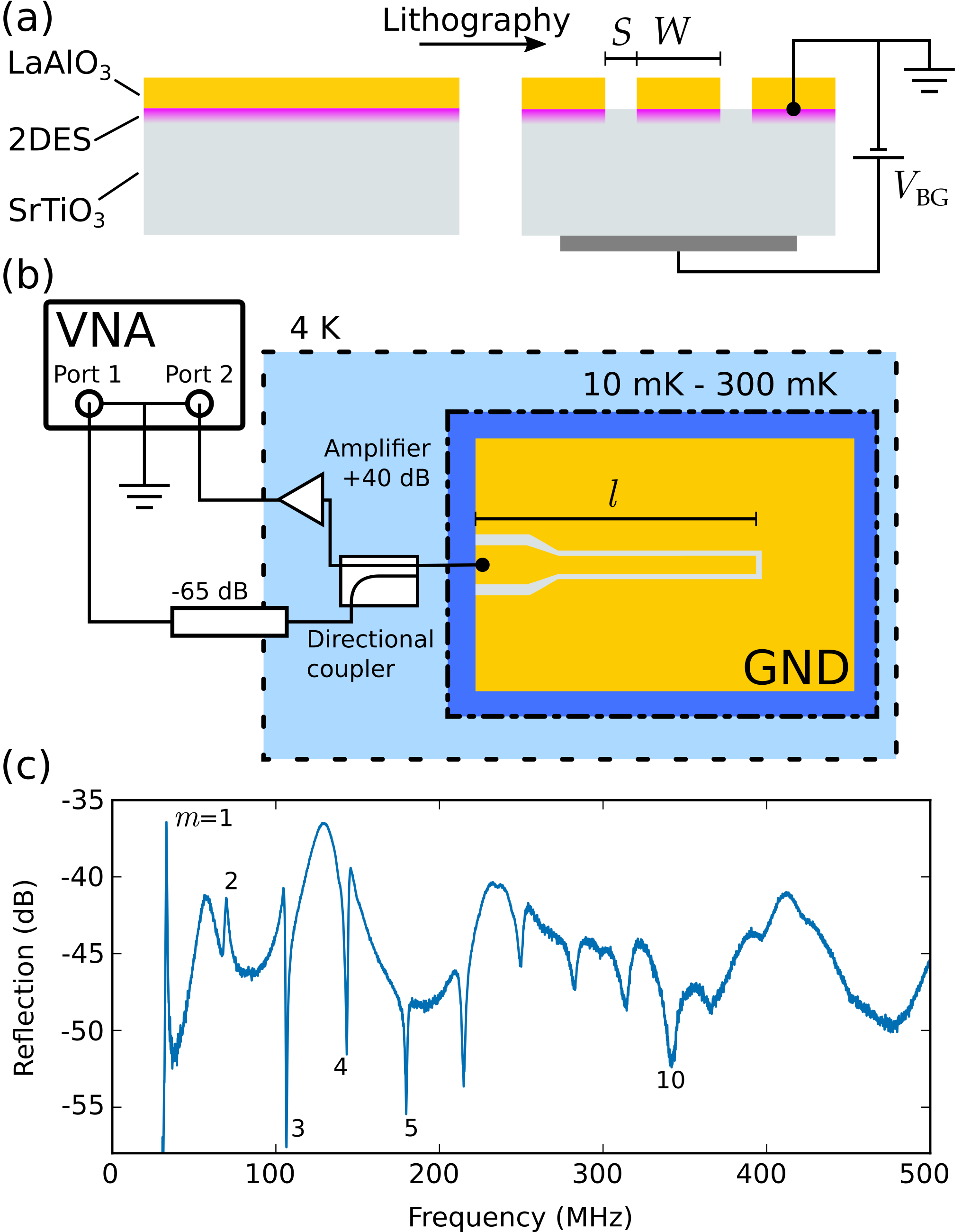
An open-end half-wavelength resonator excited at the eigenfrequency can be modeled as a parallel RLC circuit with the resonance frequency , where the inductance is mode dependent Göppl et al. (2008). In general, the inductance of a superconducting resonator is given by both a geometric and a kinetic contribution Watanabe et al. (1994). In our SCWR, already the first mode has a total geometric inductance of about 0.16 nH, while the kinetic inductance at mK (the lowest value) is about 4 nH. is thus dominated by the kinetic contribution, similarly to what has been observed in other LAO/STO superconducting devices Copie et al. (2009); Goswami et al. (2016). This allows us to write the two simple following expressions for the Pearl length and the 2D superfluid density :
| (1) | ||||
| (2) |
where and are determined by the line geometry, the dielectric environment and the effective mass of the charge carriers, as discussed in Supplemental Material, Sec. 2. By monitoring the magnitude of as a function of and , it is thus possible to investigate their effect on the superconducting state of the 2DES. The high sensitivity of this probing technique is due to the low density of Cooper pairs and the consequent high kinetic inductance of the 2DES. However, we note that the calculated values of the suffer from two main sources of error. First, the two ends of the line are not perfect mirrors and the values of are thus influenced by both the geometry of the launcher and the capacitance of the bonding pad. Second, the size of the bonding wires connecting the line leads to an estimation of its effective length of 2.380.12 mm (see Supplemental Material, Sec. 1). We thus consider a confidence interval of for the calculated absolute values of and .
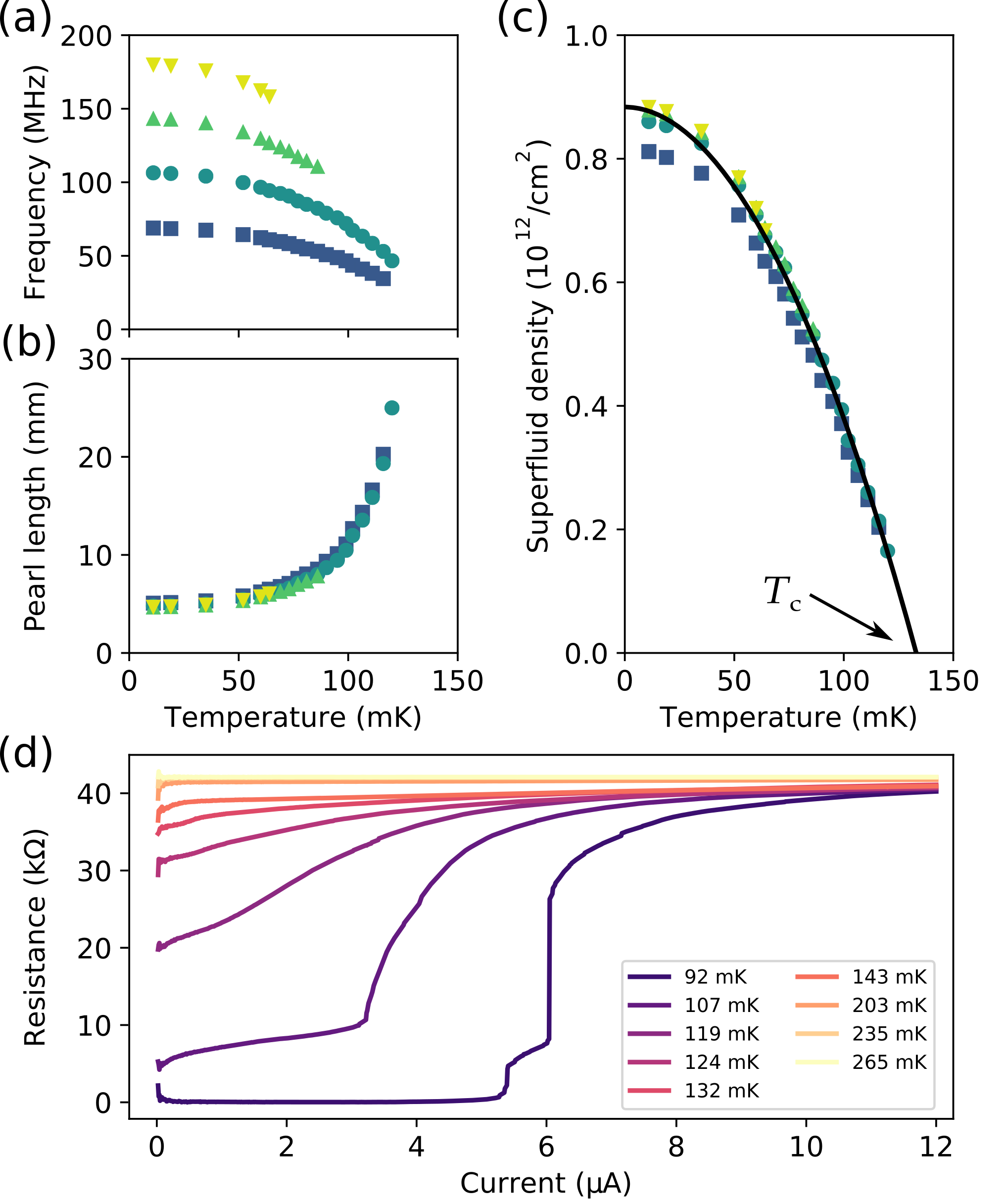
Figure 2(a) shows the temperature dependence of the cavity modes of the SCWR from to at V. All the modes are evenly spaced and their relative variations are in good agreement. The disappearance of the cavity modes above 120 mK comes from the increased power dissipation associated with the formation of quasi-particles while approaching the superconducting transition. In the normal state this device shows no resonance peaks, owing to the high resistivity of the metallic LAO/STO. From Eqs. (1) and (2) it is possible to extract the temperature dependence of and from the frequencies of each cavity mode. The calculated values are plotted in Figs. 2(b) and 2(c), respectively. At base temperature we have mm, in good agreement to what was estimated in Ref. Goswami et al., 2016, that increases to above 23 mm at 120 mK. An opposite trend is observed for , which starts from 0.871012 cm-2 at 11 mK with a negative slope that becomes progressively more pronounced. We fit the temperature dependence of with a phenomenological BCS model
| (3) |
where is the the zero-temperature superfluid density, is the superconducting critical temperature and is an exponent which describes the opening of the gap below Prozorov and Giannetta (2006); Bert et al. (2012). The black solid line in Fig. 2(c) is the best fit of Eq. (3) calculated for the third mode (circles in Fig. 2). If we consider both the second and third mode, which show the best visibility in temperature, we obtain and , respectively. These results are in fairly good agreement with a clean s-wave BCS scenario, where a value of is predicted Prozorov and Giannetta (2006). This is in contrast with previous works reporting Bert et al. (2012) and a possible indication of lower disorder in our sample Carbotte (1990). The calculated critical temperature is mK, that we can compare with the transport measurements of Fig 2(d) performed by wire-bonding the ground plane (see also the Supplementary Material, Sec. 2). The electrical resistance is current-dependent below 132 mK and a sharp transition is observed below 119 mK. Although a quantitative analysis is not possible because of the inhomogeneous current flow, we can consider the as the temperature at which the electrical resistance at zero bias reaches half of its normal state, obtaining 120 mK, in good agreement with the temperature dependence of the SCWR cavity modes.
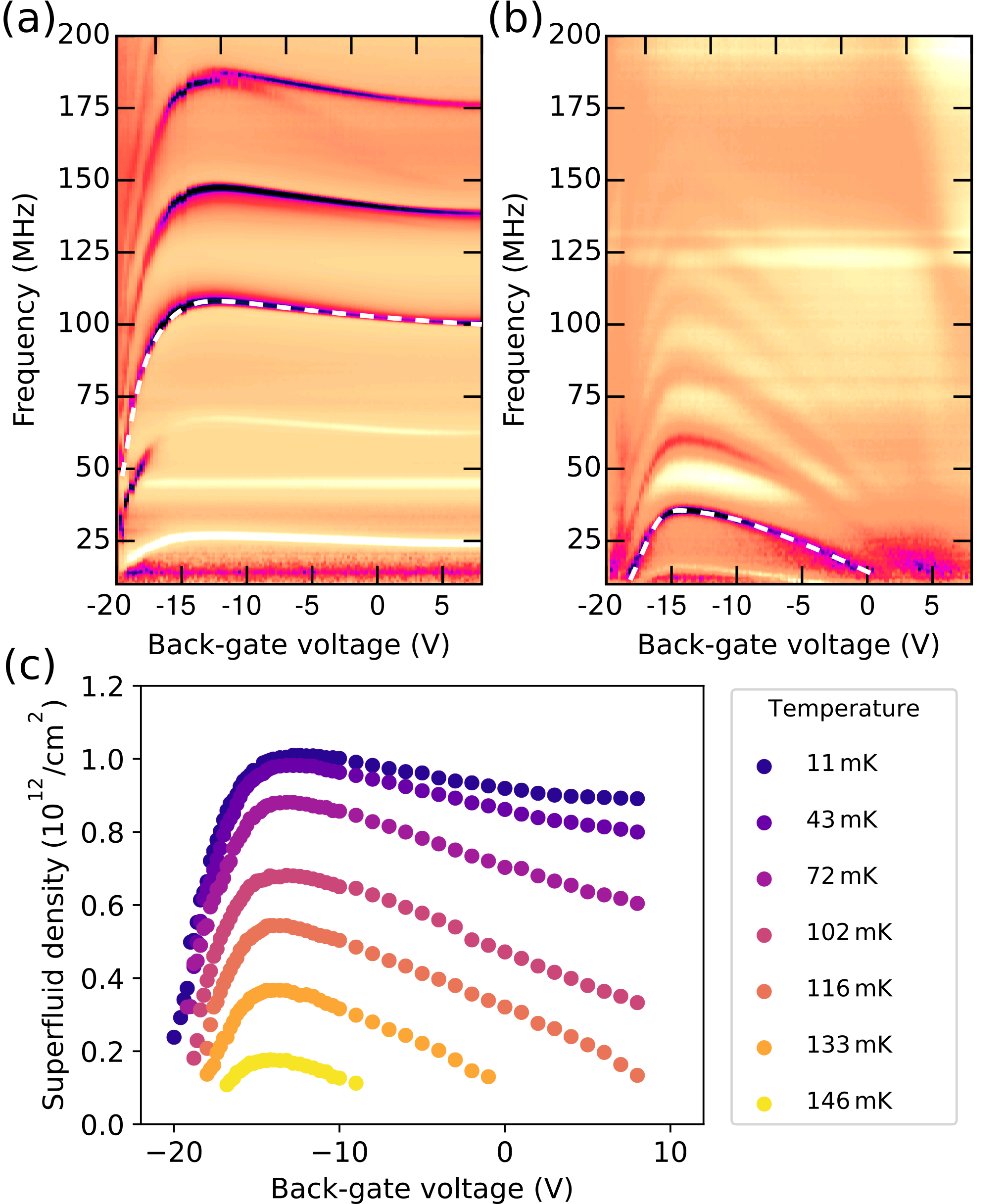
Our experimental configuration enables tuning the superfluid density of the 2DES by electric field effect. In Figure 3(a) and (b) we show two colour maps of the spectral response of the SCWR measured at 11 mK and 133 mK as a function of . At the base temperature, when the gate voltage goes below V the cavity modes rapidly shift to low frequencies and then disappear, while at positive voltages the response is rather flat with a slightly decreasing trend. At 133 mK, instead, the superconductivity can be quenched on both ends of the phase diagram with all the modes showing a pronounced dome-like response. This response originates from the modulation of , and a possible contribution to the observed signal from the the electric-field dependence of the STO dielectric constant Neville et al. (1972); Hemberger et al. (1995); Davidovikj et al. (2017) is discussed and ruled out in the Supplementary Material, Sec. 4. Similarly to the analysis reported in Fig. 2, we calculate the voltage dependence of at different temperatures using Eq. (2). Here, we base our analysis on the third mode (), which shows the best visibility over the whole space of parameters, while a complete dataset of the first five modes is reported in the Supplementary Material, Sec. 5. The phase diagram of the superfluid density reported Fig. 3(c) is characterized by a dome-like shape that becomes progressively lower and narrower for increasing temperatures. It peaks at about 12.5 V, where superconductivity is still detected at 146 mK, well above mK calculated from Fig. 2(c) and indicating that the pristine 2DES is in the over-doped regime. The maximum value of the Cooper pairs density is , corresponding to an electron density of . This is in agreement with previous experiments Bert et al. (2012); Joshua et al. (2012); Maniv et al. (2015); Singh et al. (2018), supporting the conclusion that only a small fraction of charge carriers participate to the superconductivity.
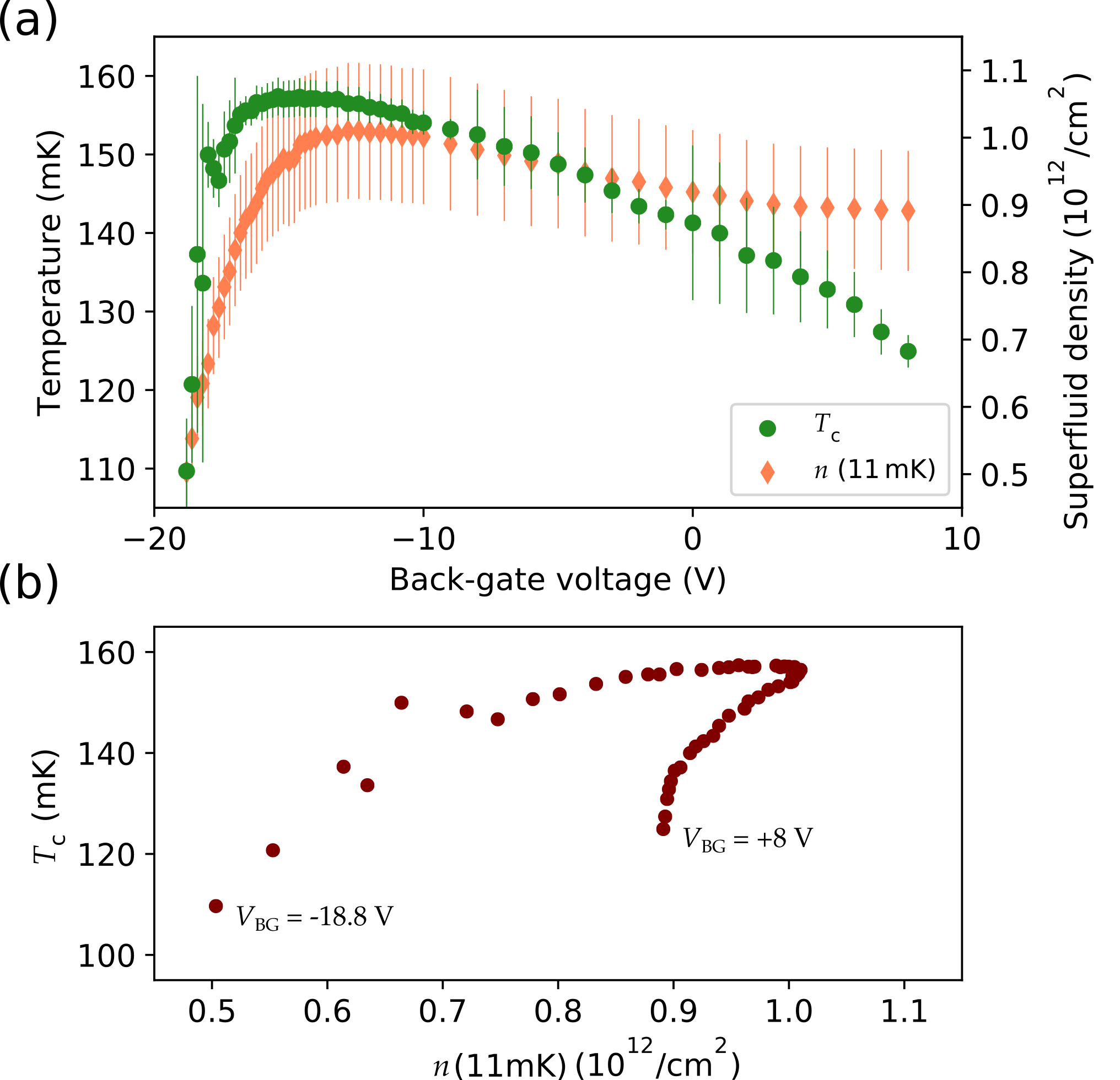
In Figure 4(a) we compare the effect of on at the base temperature and , where the latter was calculated by fitting the data reported in Fig. 3 with Eq. (3). Both of them display a well-defined dome-shape dependence, with a maximum at 12.5 V. The different position of their maximal value comes from a progressive shift of the maximum of with temperature and is discussed in the Supplementary Material, Sec. 6. Different explanations have been proposed to this peculiar phase diagram. The peak of the has been ascribed to the Lifshitz transition, where the over-doped regime is a consequence of the onset of population of , bands Joshua et al. (2012), to low-density carriers located in a high-mobility band showing non-monotonic population under field-effect due to the interplay of orbital effects and correlations Maniv et al. (2015), or a combination between the multi-band nature of this 2DES, electronic correlations, and disorder Singh et al. (2018); Trevisan et al. (2018). The interplay between and can be further investigated considering the – plot in Fig. 4(b). An upper and lower branch appear, corresponding to the over- and under-doped condition and connected at 12 V (optimal doping). A similar bimodal distribution was also reported by Bert et al. (grey dataset of Fig. 3 in Ref. Bert et al. (2012)) and ascribed to inhomogeneities that locally suppress in the over-doped regime. In our case this interpretation is at variance with the results from Fig. 2(c), where the the critical exponent 2 indicates low disorder.
The data presented in this work allows one to view the superconducting phase as the ground state of a Josephson junction array. For zero gate voltage, Fig. 2(d) shows that increasing the current in the device produces dissipation above a temperature-dependent threshold. Upon further increase of , one observes a steep rise in the resistance beyond a second threshold, and ultimately levels off to its normal state value. In the Josephson junction language a BKT-like transition takes place at the lower threshold value , where represents the typical maximum supercurrent of a junction, is the Josephson coupling and is the flux quantum Lobb et al. (1983). The dielectric constant, , jumps from a finite value to infinity at the transition (strictly speaking this only holds at K) and dissipation sets in above . For still larger values of the current, individual junctions in the array can sustain phase coherence (short-range order) as long as <. For , the array eventually crosses over to the normal state. In the intermediate regime, one may then define a bare (unrenormalized) density of Cooper pairs Lobb et al. (1983) such that
| (4) |
From Fig. 2(d) we determine . This number is in line with the ratio that one can extract from the temperature dependence of the cavity modes in Fig. 2(c), which is . From Fig. 2(d) we see that for increasing temperatures and are no more distinguishable and goes to zero together with . The temperature dependence of reported in Fig. 2(c) (overdoped condition) can be thus interpreted as a regime where the superconducting islands are large enough to sustain long-range coherence and follows the simple BCS model of Eq. (3), that in this case was found compatible with a clean s-wave superconductor. In the under-doped condition the lowered electron density makes the superconducting puddles to lose connection, resulting in a transition dominated by short-range order. This picture explains the two branches of Fig. 4(b), originating form the different nature of the ground state in the two regimes, in agreement with recent experimental results Biscaras et al. (2013); Chen et al. (2018). We may now justify the fact that transport properties of the 2DEG in this device can be related to their counterpart in Josephson junction networks. In Fig. 2(d) the steep rise in the resistance at mK is observed at µA. The equations leading to Eq. (4) also predict that the value of the critical current per junction is 37 nA and 20 nA, suggesting that about 150 parallel channels are contributing to the electrical current.
Below K, STO undergoes a structural transition from a cubic to a tetragonal phase Unoki and Sakudo (1967); Roy et al. (2017). Current maps of charge flow in \ceLAO / STO reveals a filamentary structure of the pattern which is related to the striped electrostatic potential modulation arising from the tetragonal domains in \ceSTO at low temperature Frenkel et al. (2016, 2017); Honig et al. (2013); Noad et al. (2018); Pai et al. (2018). However, the spatial resolution is not sufficient to simultaneously image the current paths and the domain boundaries; the size of the latter does not exceed 500–600 nm. Estimations of the wall (twins, dislocations) widths in the bundles reported by several authors are between few tens of nanometers Frenkel et al. (2017); Honig et al. (2013) and 1–10 nm Szot et al. (2006); Schiaffino and Stengel (2017). If the conducting channel consists of a bundle of filaments of micrometer size, one could consider each filament as forming a junction neighbouring filaments being separated by 10 nm walls. By considering about 150 parallel junctions, one recovers an approximate size of a few microns for the bundle.
In conclusion, we studied the superfluid density at the LAO/STO interface by means of a coplanar waveguide resonator patterned into the heterostructure itself. With no gate applied, the temperature dependence of the superfluid density is in good agreement with a clean s-wave BCS superconductor, while under field effect both the critical temperature and the superfluid density show a dome-shaped phase diagram, leading to a multi-valued relationship between them. The comparison between transport data and cavity resonances suggests that the ground state of this 2DES is a Josephson junction array undergoing a transition between long- and short-range order under electrostatic doping. We foresee future experiments taking advantage of the high sensitivity of this technique, as an example by combining superconducting resonators and magnetotransport measurements to explore different oxide-based 2DES.
Acknowledgements
The research leading to these results has received funding from the European Research Council under the European Union’s H2020 programme/ERC Grant Agreement No. 677458, the project Quantox of QuantERA ERA-NET Cofund in Quantum Technologies, the Netherlands Organisation for Scientific Research (NWO/OCW) as part of the Frontiers of Nanoscience program (NanoFront), and by the Dutch Foundation for Fundamental Research on Matter (FOM)
Open Data
The numerical data shown in figures of the manuscript and the supplemental material can be donwloaded from the Zenodo online repository: http://dx.doi.org/10.5281/zenodo.2530003
References
- Ohtomo and Hwang (2004) A. Ohtomo and H. Y. Hwang, Nature 427, 423 (2004).
- Cen et al. (2009) C. Cen, S. Thiel, J. Mannhart, and J. Levy, Science (80-. ). 323, 1026 (2009).
- Reyren et al. (2007) N. Reyren, S. Thiel, A. D. Caviglia, L. Fitting Kourkoutis, G. Hammerl, C. Richter, C. W. Schneider, T. Kopp, A.-S. Rüetschi, D. Jaccard, M. Gabay, D. A. Muller, J.-M. Triscone, and J. Mannhart, Science (80-. ). 317, 1196 (2007), arXiv:arXiv:1011.1669v3 .
- Ben Shalom et al. (2010) M. Ben Shalom, M. Sachs, D. Rakhmilevitch, A. Palevski, and Y. Dagan, Phys. Rev. Lett. 104, 126802 (2010), arXiv:1001.0781 .
- Diez et al. (2015) M. Diez, A. M. R. V. L. Monteiro, G. Mattoni, E. Cobanera, T. Hyart, E. Mulazimoglu, N. Bovenzi, C. W. J. Beenakker, and A. D. Caviglia, Phys. Rev. Lett. 115, 016803 (2015), arXiv:1412.5614 .
- Bert et al. (2011) J. A. Bert, B. Kalisky, C. Bell, M. Kim, Y. Hikita, H. Y. Hwang, and K. a. Moler, Nat. Phys. 7, 767 (2011), arXiv:1108.3150 .
- Li et al. (2011) L. Li, C. Richter, J. Mannhart, and R. C. Ashoori, Nat. Phys. 7, 762 (2011), arXiv:1105.0235 .
- Ohshima et al. (2017) R. Ohshima, Y. Ando, K. Matsuzaki, T. Susaki, M. Weiler, S. Klingler, H. Huebl, E. Shikoh, T. Shinjo, S. T. B. Goennenwein, and M. Shiraishi, Nat. Mater. 16, 609 (2017), arXiv:1601.07568 .
- Caviglia et al. (2008) A. D. Caviglia, S. Gariglio, N. Reyren, D. Jaccard, T. Schneider, M. Gabay, S. Thiel, G. Hammerl, J. Mannhart, and J.-M. Triscone, Nature 456, 624 (2008), arXiv:0807.0585 .
- Bell et al. (2009) C. Bell, S. Harashima, Y. Kozuka, M. Kim, B. G. Kim, Y. Hikita, and H. Y. Hwang, Phys. Rev. Lett. 103, 226802 (2009), arXiv:0906.5310 .
- Caviglia et al. (2010) A. D. Caviglia, M. Gabay, S. Gariglio, N. Reyren, C. Cancellieri, and J.-M. Triscone, Phys. Rev. Lett. 104, 126803 (2010), arXiv:0912.3731v1 .
- Monteiro et al. (2017) A. M. R. V. L. Monteiro, D. J. Groenendijk, N. Manca, E. Mulazimoglu, S. Goswami, Y. Blanter, L. M. K. Vandersypen, and A. D. Caviglia, Nano Lett. 17, 715 (2017), arXiv:1609.03304 .
- Goswami et al. (2016) S. Goswami, E. Mulazimoglu, A. M. R. V. L. Monteiro, R. Wölbing, D. Koelle, R. Kleiner, Y. M. Blanter, L. M. K. Vandersypen, and A. D. Caviglia, Nat. Nanotechnol. 11, 861 (2016), arXiv:1512.04290 .
- Thierschmann et al. (2018) H. Thierschmann, E. Mulazimoglu, N. Manca, S. Goswami, T. M. Klapwijk, and A. D. Caviglia, Nat. Commun. 9, 2276 (2018).
- Bert et al. (2012) J. A. Bert, K. C. Nowack, B. Kalisky, H. Noad, J. R. Kirtley, C. Bell, H. K. Sato, M. Hosoda, Y. Hikita, H. Y. Hwang, and K. A. Moler, Phys. Rev. B 86, 060503 (2012).
- Singh et al. (2018) G. Singh, A. Jouan, L. Benfatto, F. Couëdo, P. Kumar, A. Dogra, R. C. Budhani, S. Caprara, M. Grilli, E. Lesne, A. Barthélémy, M. Bibes, C. Feuillet-Palma, J. Lesueur, and N. Bergeal, Nat. Commun. 9, 407 (2018), arXiv:1704.03365 .
- Lancaster et al. (1998) M. J. Lancaster, J. Powell, and A. Porch, Supercond. Sci. Technol. 11, 1323 (1998).
- Tiggelman et al. (2009) M. P. J. Tiggelman, K. Reimann, F. Van Rijs, J. Schmitz, and R. J. E. Hueting, IEEE Trans. Electron Devices 56, 2128 (2009).
- Ahmed et al. (2015) A. Ahmed, I. A. Goldthorpe, and A. K. Khandani, Appl. Phys. Rev. 2, 0 (2015).
- Baselmans et al. (2007) J. Baselmans, S. Yates, P. de Korte, H. Hoevers, R. Barends, J. Hovenier, J. Gao, and T. Klapwijk, Adv. Sp. Res. 40, 708 (2007).
- Vercruyssen et al. (2011) N. Vercruyssen, R. Barends, T. M. Klapwijk, J. T. Muhonen, M. Meschke, and J. P. Pekola, Appl. Phys. Lett. 99, 062509 (2011).
- Nataf and Ciuti (2011) P. Nataf and C. Ciuti, Phys. Rev. Lett. 107, 190402 (2011).
- Xiang et al. (2013) Z.-L. Xiang, S. Ashhab, J. Q. You, and F. Nori, Rev. Mod. Phys. 85, 623 (2013), arXiv:1204.2137 .
- Chow et al. (2014) J. M. Chow, J. M. Gambetta, E. Magesan, D. W. Abraham, A. W. Cross, B. R. Johnson, N. A. Masluk, C. A. Ryan, J. A. Smolin, S. J. Srinivasan, and M. Steffen, Nat. Commun. 5, 1 (2014), arXiv:1311.6330 .
- Baselmans et al. (2008) J. Baselmans, S. J. C. Yates, R. Barends, Y. J. Y. Lankwarden, J. R. Gao, H. Hoevers, and T. M. Klapwijk, J. Low Temp. Phys. 151, 524 (2008).
- Bueno et al. (2017) J. Bueno, O. Yurduseven, S. J. C. Yates, N. Llombart, V. Murugesan, D. J. Thoen, A. M. Baryshev, A. Neto, and J. J. A. Baselmans, Appl. Phys. Lett. 110, 233503 (2017).
- Davidovikj et al. (2017) D. Davidovikj, N. Manca, H. S. J. van der Zant, A. D. Caviglia, and G. A. Steele, Phys. Rev. B 95, 214513 (2017), arXiv:1607.08146 .
- Göppl et al. (2008) M. Göppl, A. Fragner, M. Baur, R. Bianchetti, S. Filipp, J. M. Fink, P. J. Leek, G. Puebla, L. Steffen, and A. Wallraff, J. Appl. Phys. 104, 113904 (2008).
- Watanabe et al. (1994) K. Watanabe, K. Yoshida, T. Aoki, and S. Kohjiro, Jpn. J. Appl. Phys. 33, 5708 (1994).
- Copie et al. (2009) O. Copie, V. Garcia, C. Bodefeld, C. Carrétéro, M. Bibes, G. Herranz, E. Jacquet, J.-L. Maurice, B. Vinter, S. Fusil, K. Bouzehouane, H. Jaffrès, and A. Barthélémy, Phys. Rev. Lett. 102, 216804 (2009), arXiv:0905.2049 .
- Prozorov and Giannetta (2006) R. Prozorov and R. W. Giannetta, Supercond. Sci. Technol. 19, R41 (2006), arXiv:0605612 [cond-mat] .
- Carbotte (1990) J. P. Carbotte, Rev. Mod. Phys. 62, 1027 (1990).
- Neville et al. (1972) R. C. Neville, B. Hoeneisen, and C. A. Mead, J. Appl. Phys. 43, 2124 (1972), arXiv:arXiv:1011.1669v3 .
- Hemberger et al. (1995) J. Hemberger, P. Lunkenheimer, R. Viana, R. Böhmer, and A. Loidl, Phys. Rev. B 52, 13159 (1995).
- Joshua et al. (2012) A. Joshua, S. Pecker, J. Ruhman, E. Altman, and S. Ilani, Nat. Commun. 3, 1129 (2012), arXiv:1110.2184 .
- Maniv et al. (2015) E. Maniv, M. Ben Shalom, A. Ron, M. Mograbi, A. Palevski, M. Goldstein, and Y. Dagan, Nat. Commun. 6, 8239 (2015), arXiv:1509.03449 .
- Trevisan et al. (2018) T. V. Trevisan, M. Schütt, and R. M. Fernandes, ArXiv , 1 (2018), arXiv:1803.02389 .
- Lobb et al. (1983) C. J. Lobb, D. W. Abraham, and M. Tinkham, Phys. Rev. B 27, 150 (1983).
- Biscaras et al. (2013) J. Biscaras, N. Bergeal, S. Hurand, C. Feuillet-Palma, A. Rastogi, R. C. Budhani, M. Grilli, S. Caprara, and J. Lesueur, Nat. Mater. 12, 542 (2013).
- Chen et al. (2018) Z. Chen, A. G. Swartz, H. Yoon, H. Inoue, T. Merz, D. Lu, Y. Xie, H. Yuan, Y. Hikita, S. Raghu, and H. Y. Hwang, , 1 (2018), arXiv:1807.08347 .
- Unoki and Sakudo (1967) H. Unoki and T. Sakudo, J. Phys. Soc. Japan 23, 546 (1967).
- Roy et al. (2017) D. Roy, Y. Frenkel, S. Davidovitch, E. Persky, N. Haham, M. Gabay, B. Kalisky, and L. Klein, Phys. Rev. B 95, 245303 (2017).
- Frenkel et al. (2016) Y. Frenkel, N. Haham, Y. Shperber, C. Bell, Y. Xie, Z. Chen, Y. Hikita, H. Y. Hwang, and B. Kalisky, ACS Appl. Mater. Interfaces 8, 12514 (2016).
- Frenkel et al. (2017) Y. Frenkel, N. Haham, Y. Shperber, C. Bell, Y. Xie, Z. Chen, Y. Hikita, H. Y. Hwang, E. K. Salje, and B. Kalisky, Nat. Mater. 16, 1203 (2017).
- Honig et al. (2013) M. Honig, J. A. Sulpizio, J. Drori, A. Joshua, E. Zeldov, and S. Ilani, Nat. Mater. 12, 1112 (2013), arXiv:1312.3343 .
- Noad et al. (2018) H. Noad, P. Wittlich, J. Mannhart, and K. A. Moler, (2018), arXiv:1805.08549 .
- Pai et al. (2018) Y.-Y. Pai, H. Lee, J.-W. Lee, A. Annadi, G. Cheng, S. Lu, M. Tomczyk, M. Huang, C.-B. Eom, P. Irvin, and J. Levy, Phys. Rev. Lett. 120, 147001 (2018).
- Szot et al. (2006) K. Szot, W. Speier, G. Bihlmayer, and R. Waser, Nat. Mater. 5, 312 (2006).
- Schiaffino and Stengel (2017) A. Schiaffino and M. Stengel, Phys. Rev. Lett. 119, 137601 (2017).
See pages 1 of LAO_STO_CPW-reviewed-supplementary.pdf See pages 2 of LAO_STO_CPW-reviewed-supplementary.pdf See pages 3 of LAO_STO_CPW-reviewed-supplementary.pdf See pages 4 of LAO_STO_CPW-reviewed-supplementary.pdf See pages 5 of LAO_STO_CPW-reviewed-supplementary.pdf See pages 6 of LAO_STO_CPW-reviewed-supplementary.pdf See pages 7 of LAO_STO_CPW-reviewed-supplementary.pdf See pages 8 of LAO_STO_CPW-reviewed-supplementary.pdf See pages 9 of LAO_STO_CPW-reviewed-supplementary.pdf See pages 10 of LAO_STO_CPW-reviewed-supplementary.pdf