Current address: ]Institute of Electronics, Atomic Energy Research Establishment, Savar, Dhaka 1349, Bangladesh
Current address: ]Korea Research Institute of Standards and Science, Dajeon 34113, Korea
Silicon photonic crystal cavities at near band-edge wavelengths
Abstract
We demonstrate photonic crystal L3 cavities with resonant wavelength around 1.078 µm on undoped silicon-on-insulator, designed to enhance spontaneous emission from phosphorus donor-bound excitons. We have optimised a fabrication recipe using readily available process materials such as polymethyl methacrylate (PMMA) as a soft electron-beam mask and a Chemical Vapour Deposition (CVD) grown oxide layer as a hard mask. Our bilayer resist technique efficiently produces photonic crystal cavities with a quality factor () of at a wavelength of µm, measured using cavity reflection measurements at room temperature. We observe a decrease of as the cavity resonance shifts to shorter wavelengths ( at wavelengths µm), which is mostly due to the intrinsic absorption of silicon.
Defect spins in solid state materials are attractive candidates for scalable implementation and integration of quantum information processing (QIP)Ladd et al. (2010); Gordon et al. (2013), metrology Bonato et al. (2016); Wolfowicz, Whiteley, and Awschalom (2018); Tarasenko et al. (2018) and communication systems Blok et al. (2015); Johnson, Dolan, and Smith (2017). For example, coherent spins in diamond and their interactions with photons have been exploited for optically-mediated entanglement of matter-based systems Bernien et al. (2013); Pfaff et al. (2014). While nitrogen-vacancy (NV) centres in diamond possess many attractive features that have underpinned key quantum information/communication demonstrations, some of the optical properties are sub-optimal (broad phonon sideband and spectral broadening) while thin-film growth and fabrication processes still need to be perfected. For such reasons, other materials systems combining excellent optical and spin memory properties with mature fabrication techniques are being explored to develop effective spin-photon interfacesGordon et al. (2013); Atatüre et al. (2018); Christle et al. (2017); Zhong et al. (2015). Amongst these have been vacancies in silicon carbide (SiC) and defects in silicon (Si). Silicon and SiC host defects and impurities with long spin coherence time Steger et al. (2012); Christle et al. (2017) and narrow linewidth emission of photons Yang et al. (2006); Thewalt et al. (2007); Steger et al. (2011); Christle et al. (2017) and permit coherent optical control of spins Zwier et al. (2015). These features, combined with the mature industrial techniques in manufacturing and on-chip integration, make such spins attractive for efficient multi-qubit coupling and realising large scale QIP systems. However, strong non-radiative processes in silicon-based host materials restrict fluorescence efficiency Schmid (1977); Thewalt et al. (2007); Sumikura et al. (2011) and indistinguishable single photon generation Pelton et al. (2002); Christle et al. (2017), thus limiting the potential of optical interfaces with most defects in silicon. This issue can, in principle, be addressed by engineering the local photonic environment in the host material: for example, incorporating photonic structures such as circular Bragg resonators (CBRs) Davanço et al. (2011) or photonic crystal cavities (PCCs) Joannopoulos, Villeneuve, and Fan (1997); Faraon et al. (2012) can enhance photon emission and collection efficiency by several orders of magnitude, potentially allowing it to compete with non-radiative processes such as Auger recombination.
Enhanced light-matter interaction in PCCsJoannopoulos, Villeneuve, and Fan (1997) has been demonstrated for various quantum emitters including NV centers in diamond Faraon et al. (2012), rare-earth-doped crystals Zhong et al. (2015) and quantum dots in GaAsReinhard et al. (2011), with observed improvements in the radiative emissionZhong et al. (2015); Lee et al. (2015). Similar schemes with PCCs can be utilised to enhance defect related emission in Si Fu et al. (2004) and SiC Calusine, Politi, and Awschalom (2014, 2016) systems. Several defects such as shallow donors in silicon Dean, Haynes, and Flood (1967); Yang et al. (2006); Thewalt et al. (2007) and divacancyChristle et al. (2017); Lohrmann et al. (2017), transition metal Baur, Kunzer, and Schneider (1997); Son et al. (1999), and Ky5 color centre Son et al. (1996); Calusine, Politi, and Awschalom (2016) defects in SiC Lohrmann et al. (2017) manifest spin-coupled optical emission with wavelength near µm (i.e. near the silicon band-edge). PCCs with a high ratio of Q-factor to mode volume () could be used to develop efficient spin-photon interfaces to such defects, however, experimental studies in this wavelength range on such materials are limited. In SiC, planar PCCs with wavelengths in the range 1100–1300 nm have been fabricatedCalusine, Politi, and Awschalom (2014, 2016) with , but the band-gap of Si is substantially smaller and there are significant challenges related to absorption when the PCC resonance approaches the band-gap energy. Photon absorption from the host material leads to uncertainties in the photonic modes and photonic band-gap as compared to non-dispersive materialsSakoda (2005), and detection of weak optical signals near the silicon band-edge is made more challenging due to the low quantum efficiency of Si detectors or the high dark count in InGaAs detectorsDussault and Hoess (2004).
Here, we design, fabricate and study suspended Si PCCs, made from silicon-on-insulator (SOI) substrates, with wavelengths in the range 1065–1085 nm at room temperature. We incorporate fine-tuning and band-folding in our L3 cavities in order to achieve high quality factors and better extraction of light, which could be utilised to enhance shallow impurity spontaneous emissions such as donor bound exciton (31P D0X D0) transitions in silicon. We have optimised a fabrication recipe using relatively inexpensive process materials in order to realise Si PCCs using a conventional etching/pattern transfer processes. Finally, we used cross-polarisation confocal microscopyFaraon et al. (2008); Galli et al. (2009) with a broadband source and a spectrograph with low-noise Si detector array to measure PCC reflection spectra, observing PCC Q-factors in the range 2,600 to 6,200, increasing with cavity wavelength.
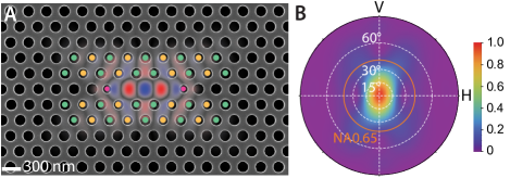
L3 cavities are implemented by removing a row of three air holes from the hexagonal photonic crystal (PhC) lattice with lattice constant . We systematically study near Si band-edge resonant modes by fabricating L3 PCCs with lattice constants ranging from = 240 to 300 nm. The L3 fundamental mode ()[Chalcraft et al. (2007)] can be further engineered to improve and light outcoupling, while keeping the mode volume below . can be increased by changing position and/or size of one or more side-holes adjacent to the cavityAkahane et al. (2005). The position displacement of any side hole from its original location in the lattice is indicated by a shift, and any absolute change in the corresponding hole radius by, . Figure 1(a) shows the SEM image of an L3 cavity where the position and size of a pair of holes (marked in red) on either side of the cavity has been adjusted ( and ). Such a change in the design can produce as high as [Akahane et al. (2005)].
The vertical collection efficiency () is improved by implementing a band folding schemeTran, Combrié, and De Rossi (2009); Portalupi et al. (2010) in which gratings of periodicity are superimposed on the PhC lattice by modulating the radii of certain holes in the vicinity of the cavity. In Figure 1(a), the radius of the green set of holes above and below the cavity is increased () from the regular air hole radius of while the radius of the yellow marked holes is reduced (). The incorporation of such a hole-size modulation in the design limits , but increases up to 0.8 for an NA = 0.65 (see Figure 1(b)), where NA is the numerical aperture of the collection objective. These mode properties were simulated based on data extracted from SEM images of fabricated structures, and are similar to those based on the idealised design. This indicates fabrication errors are unlikely to be a significant contribution to collection losses. We have also implemented designs with three side hole shifts (, and ) and a slightly modified modulation scheme in which the radii of the green holes remain at , while the yellow have a larger radius (). This modified hole modulation scheme, in principle, can further improve while maintaining collection efficiencies of for an NA = 0.65.
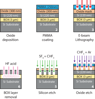
We optimised fabrication process steps to transfer e-beam lithography (EBL, at 30 kV) profiles into the thin (220 nm) Si device layer of the SOI chip with minimum distortions. Effective realisation of Si PhCs with small lattice constants ( nm) depends on the availability of a lithographic mask that can withstand plasma etching long enough to transfer the patterns efficiently to the 220 nm Si layer Bailey III et al. (1998). We adopted a bilayer resist of polymethyl methacrylate (250 nm) and PECVD grown oxide layer (300 nm), which is less affected by proximity effects and can provide sufficient etch selectivity and anisotropy for the plasma etch steps under consideration. The process recipe includes two steps of reactive ion etching (RIE): CHF3/Ar plasma to transfer the pattern on the oxide layer and CHF3/SF6 plasma to etch the silicon layer. Conditions for anisotropic etching have been obtained by further adjusting RIE parameters including flow rates (CHF3 - 25 sccm & Ar - 25 sccm), RF power (150W), and pressure (30 mT) for oxide etch and flow rates (CHF3 - 58 sccm & SF6 - 25 sccm), RF power (150W), and pressure (10 mT) for silicon etch. We run a cooling step (50 sccm Ar flow without plasma) for two minutes after each 30 s long plasma etching step to avoid PMMA deformations by heat, and repeat this cycle 24 times until the pattern penetrates through the 300 nm oxide hard mask layer. Finally, the pattern is transferred to the 220 nm Si device layer using plasma etch along with the oxide hard mask. To release the suspended membrane containing the PhC, we undercut the buried oxide (BOX) layer of the SOI chip and remove remaining oxide masks together with hydrofluoric acid (HF). The major process steps in the optimised fabrication recipe are shown in Figure 2. When the fabricated devices are inspected under SEM, it is found that fabrication errors are small. The hole radii in the silicon membrane were larger than the intended values by less than 10 nm, producing good PhCs with lattice constants between 240 and 300 nm.
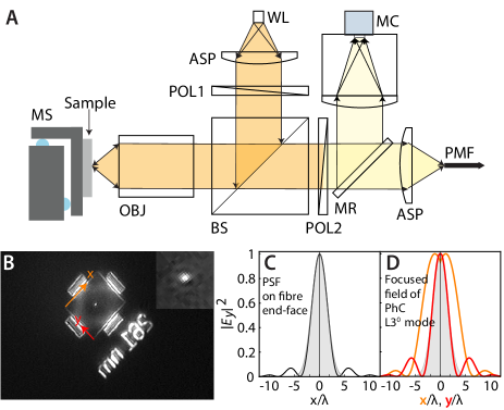
Fabricated Si PCCs were characterised by cavity reflection measurements using a cross-polarisation confocal setup shown in Figure 3(a). An optical image of a PCC (a bright dot in centre of the rectangle) captured by the CMOS camera (CM) is shown in Figure 3(b). The cavity reflection signal was collected into a single mode polarisation maintaining fibre (PMF) in a confocal configuration where the point spread function is matched to the fibre mode, as shown in Figure 3(c), with a spatial resolution Novotny and Hecht (2006), µm determined for a high numerical aperture (NA = 0.65) and an excitation wavelength () of µm. The maximum coupling efficiency was measured to be 70% using the Gaussian beam collimated from a single mode fibreKowalevicz Jr and Bucholtz (2006). The cross-polarisation setup was implemented by setting the two polarisers, POL1 and POL2 in orthogonal directions Faraon et al. (2008); Galli et al. (2009) (Figure 3(a)). A suppression ratio around has been measured with this system, which in turn allows to select reflections associated with the cavity mode. The bright spot shown in the camera image (Figure 3(b)) also contains signals from higher order modes and tails of the cavity resonance, resolved with a signal-to-noise ratio (SNR) of . In Figure 3(c), the black trace is the point spread function/illumination profile from the source observed at the polarisation-maintaining fibre (PMF) end, the grey area denotes the collection by the PMF. The orange and red traces in Figure 3(d) are the focussed field intensities of mode along and -axes, respectively. The field profile at the PMF end is calculated from field amplitudes and phases of the simulated far-field profile Novotny and Hecht (2006) of the cavity (Figure 1(b)). Now, cavity scattering makes the focused spot spread wider along -axis (orange trace) than along -axis (red trace) at the end of the collection PMF. This gives a broader shape for the field profile along -axis (orange trace in Figure 3(d)) than the collection by the PMF (grey shaded curves in Figure 3(c) & (d)) and causes a mode mismatch with the PMF. From the traces in Figure 3(d), we extract a mode mismatch of . Finally, by taking account of the collection efficiency of PCCs (), path losses in the optical setup, PMF coupling efficiency etc., a total coupling efficiency of has been estimated for our confocal setup.
An Acton SP-2750 Princeton Instruments spectrometer with a focal length of m was used to capture the spectrum of the collected signal. We used a 300 g/mm blaze grating optimised for wavelengths around 1 µm which can provide a resolution of approximately pm around the 31P D0X D0 transition wavelengths. The dispersed light from the grating was detected by a Si-based CCD array (PyLoN System Silicon CCD Camera) enabling the measurement of quality factors up to . The output power of the LED source used (M1050D1, Thorlabs) peaks at 50 mW, but varies considerably across the measurement window of interest (1060–1090 nm), falling to about 10 mW at the 31P D0X D0 transition wavelength.
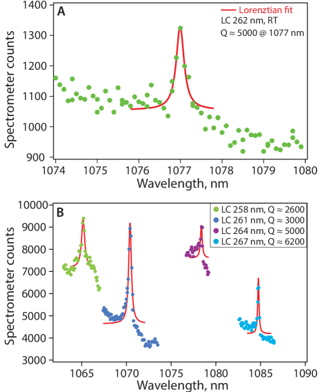
Results of cavity reflection measurements at room temperature are summarised in Figure 4. For a single side-hole shifted L3 cavity with nm, we observe the fundamental resonant mode () appearing at a wavelength of nm, which closely matches the D0X transitions in silicon. The designed for this mode is , while the Lorentzian fit to the measured data gives an experimental . Such a mismatch is often attributed to fabrication or structural imperfections in the PCCMaeno et al. (2017), however, for near band-edge Si PCCs, the intrinsic material absorption can also be a dominant loss mechanism and this was not accounted for in the simulations of the idealised structures. Silicon has an absorption coefficient cm-1) near the band-edge, at room temperatureKomma (2016); Ross (2017), giving an upper bound of only few thousand for achievable PCC values. To investigate this in greater depth, we studied three side-hole shifted L3 cavities, designed for , across a lithographic tuning range with a step size of 3 nm.
Near Si band-edge resonant modes for the three side-hole shifted L3 cavities are shown in Figure 4(b), with selected fundamental resonances () at nm, nm, nm and nm for L3 cavities with lattice constants of nm, nm, nm and nm, respectively. The quality factors () extracted from measurement data are , , and , growing with increasing wavelength. At room temperature, optical absorption in Si drops gradually with decreasing photon energies below the bandgap Komma (2016); Ross (2017), consistent with our measurements. We also note that both Si PCC designs (single- and three- side-hold shifts) show for near 31P D0X transition wavelengths ( nm), suggesting that losses in our near band-edge cavities at room temperature are dominated by intrinsic material absorption in Si. Absorption at these wavelengths in Si drops significantly at cryogenic temperatures Komma (2016); Ross (2017), and so significantly higher Q values can be expected. Low temperature PL measurements on 31P doped float zone (Fz) type Si sample, using a similar measurement setup, have shown the detection of approximately 1000 effective 31P D0X emitters in Si (ensemble linewidth of nm). Even the Q-factors of around 5000 that we measure at room temperature should be sufficient for detecting optical emission from spins down to the single or few donor/defect level in SiDean, Haynes, and Flood (1967); Yang et al. (2006) or SiC Lohrmann et al. (2017).
In summary, we have optimised a low cost fabrication process recipe for realising Si PCCs and efficiently fabricated L3 cavities with resonances near silicon band-edge wavelengths. Room temperature optical characterisation of fabricated cavities unveils an absorption-limited of 5000 with a collection efficiency close to around 1078 nm. Such near band-edge Si PCCs may play an important role in realising efficient spin-photon interfaces in Si and SiC systems.
Acknowledgements.
We thank the London Centre for Nanotechnology cleanroom staff for their technical support. We thank G. Matmon, UCL, for use of experimental equipment and insightful comments, and T. F. Krauss and C. Reardon, University of York for providing the SOI wafer and for useful discussions. The research leading to these results has received funding from the European Research Council under the European Union’s Seventh Framework Programme (FP7/2007-2013)/ ERC grant agreement No. 279781 (ASCENT) and Horizon 2020 research and innovation programme (grant agreement No. 771493 (LOQO-MOTIONS). We also acknowledge financial support from EPSRC and UCL Engineering.References
- Ladd et al. (2010) T. D. Ladd, F. Jelezko, R. Laflamme, Y. Nakamura, C. Monroe, and J. L. O’Brien, Nature 464, 45 (2010).
- Gordon et al. (2013) L. Gordon, J. R. Weber, J. B. Varley, A. Janotti, D. D. Awschalom, and C. G. Van de Walle, MRS Bulletin 38, 802 (2013).
- Bonato et al. (2016) C. Bonato, M. S. Blok, H. T. Dinani, D. W. Berry, M. L. Markham, D. J. Twitchen, and R. Hanson, Nature Nanotechnology 11, 247 (2016).
- Wolfowicz, Whiteley, and Awschalom (2018) G. Wolfowicz, S. J. Whiteley, and D. D. Awschalom, (2018), 1803.05956 .
- Tarasenko et al. (2018) S. A. Tarasenko, A. V. Poshakinskiy, D. Simin, V. A. Soltamov, E. N. Mokhov, P. G. Baranov, V. Dyakonov, and G. V. Astakhov, Physica Status Solidi (b) 255, 1700258 (2018).
- Blok et al. (2015) M. S. Blok, N. Kalb, A. Reiserer, T. H. Taminiau, and R. Hanson, Faraday Discuss. (2015), 10.1039/C5FD00113G.
- Johnson, Dolan, and Smith (2017) S. Johnson, P. R. Dolan, and J. M. Smith, Progress in Quantum Electronics 55, 129 (2017).
- Bernien et al. (2013) H. Bernien, B. Hensen, W. Pfaff, G. Koolstra, M. S. Blok, L. Robledo, T. H. Taminiau, M. Markham, D. J. Twitchen, L. Childress, and R. Hanson, Nature 497, 86 (2013).
- Pfaff et al. (2014) W. Pfaff, B. J. Hensen, H. Bernien, S. B. van Dam, M. S. Blok, T. H. Taminiau, M. J. Tiggelman, R. N. Schouten, M. Markham, D. J. Twitchen, and R. Hanson, Science 345, 532 (2014).
- Atatüre et al. (2018) M. Atatüre, D. Englund, N. Vamivakas, S.-Y. Lee, and J. Wrachtrup, Nature Reviews Materials 491, 421 (2018).
- Christle et al. (2017) D. J. Christle, P. V. Klimov, C. F. de las Casas, K. Szász, V. Ivády, V. Jokubavicius, J. U. Hassan, M. Syväjärvi, W. F. Koehl, T. Ohshima, N. T. Son, E. Janzén, Á. Gali, and D. D. Awschalom, Physical Review X 7, 021046 (2017).
- Zhong et al. (2015) T. Zhong, J. M. Kindem, E. Miyazono, and A. Faraon, Nature Communications 6, 8206 (2015).
- Steger et al. (2012) M. Steger, K. Saeedi, M. L. W. Thewalt, S. Simmons, H. Riemann, N. V. Abrosimov, P. Becker, and H. J. Pohl, Science 336, 1280 (2012).
- Yang et al. (2006) A. Yang, M. Steger, D. Karaiskaj, M. L. W. Thewalt, M. Cardona, K. M. Itoh, H. Riemann, N. V. Abrosimov, M. F. Churbanov, A. V. Gusev, A. D. Bulanov, A. K. Kaliteevskii, O. N. Godisov, P. Becker, H. J. Pohl, J. W. Ager, and E. E. Haller, Physical Review Letters 97, 227401 (2006).
- Thewalt et al. (2007) M. L. W. Thewalt, A. Yang, M. Steger, D. Karaiskaj, M. Cardona, H. Riemann, N. V. Abrosimov, A. V. Gusev, A. D. Bulanov, I. D. Kovalev, A. K. Kaliteevskii, O. N. Godisov, P. Becker, H. J. Pohl, E. E. Haller, J. W. Ager Iii, and K. M. Itoh, Journal of Applied Physics 101, 081724 (2007).
- Steger et al. (2011) M. Steger, T. Sekiguchi, A. Yang, K. Saeedi, M. E. Hayden, M. L. W. Thewalt, K. M. Itoh, H. Riemann, N. V. Abrosimov, P. Becker, and H. J. Pohl, Journal of Applied Physics 109, 102411 (2011).
- Zwier et al. (2015) O. V. Zwier, D. O’Shea, A. R. Onur, and C. H. van der Wal, Scientific Reports 5, 10931 (2015).
- Schmid (1977) W. Schmid, Physica Status Solidi (b) 84, 529 (1977).
- Sumikura et al. (2011) H. Sumikura, K. Nishiguchi, Y. Ono, A. Fujiwara, and M. Notomi, Optics Express 19, 25255 (2011).
- Pelton et al. (2002) M. Pelton, C. Santori, J. Vuckovic, B. Zhang, G. S. Solomon, J. Plant, and Y. Yamamoto, Physical Review Letters 89, 233602 (2002).
- Davanço et al. (2011) M. Davanço, M. T. Rakher, D. Schuh, A. Badolato, and K. Srinivasan, Applied Physics Letters 99, 041102 (2011).
- Joannopoulos, Villeneuve, and Fan (1997) J. D. Joannopoulos, P. R. Villeneuve, and S. Fan, Nature 386, 143 (1997).
- Faraon et al. (2012) A. Faraon, C. Santori, Z. Huang, V. M. Acosta, and R. G. Beausoleil, Physical Review Letters 109, 033604 (2012).
- Reinhard et al. (2011) A. Reinhard, T. Volz, M. Winger, A. Badolato, K. J. Hennessy, E. L. Hu, and A. Imamoglu, Nature Photonics 6, 93 (2011).
- Lee et al. (2015) C.-M. Lee, H.-J. Lim, C. Schneider, S. Maier, S. Höfling, M. Kamp, and Y.-H. Lee, Sci. Rep. 5, 14309 (2015).
- Fu et al. (2004) K.-M. C. Fu, T. D. Ladd, C. Santori, and Y. Yamamoto, Physical Review B 69, 125306 (2004).
- Calusine, Politi, and Awschalom (2014) G. Calusine, A. Politi, and D. D. Awschalom, Applied Physics Letters 105, 011123 (2014).
- Calusine, Politi, and Awschalom (2016) G. Calusine, A. Politi, and D. D. Awschalom, Physical Review Applied 6, 014019 (2016).
- Dean, Haynes, and Flood (1967) P. J. Dean, J. R. Haynes, and W. F. Flood, Physical Review 161, 711 (1967).
- Lohrmann et al. (2017) A. Lohrmann, B. C. Johnson, J. C. McCallum, and S. Castelletto, Reports on Progress in Physics 80, 034502 (2017).
- Baur, Kunzer, and Schneider (1997) J. Baur, M. Kunzer, and J. Schneider, Physica Status Solidi (a) 162, 153 (1997).
- Son et al. (1999) N. T. Son, A. Ellison, B. Magnusson, M. F. MacMillan, W. M. Chen, B. Monemar, and E. Janzén, Journal of Applied Physics 86, 4348 (1999).
- Son et al. (1996) N. T. Son, E. Sörman, W. M. Chen, M. Singh, C. Hallin, O. Kordina, B. Monemar, E. Janzén, and J. L. Lindström, Journal of Applied Physics 79, 3784 (1996).
- Sakoda (2005) K. Sakoda, Optical Properties of Photonic Crystals, Springer Series in Optical Sciences, Vol. 80 (Springer-Verlag, Berlin/Heidelberg, 2005).
- Dussault and Hoess (2004) D. Dussault and P. Hoess, in Optical Science and Technology, the SPIE 49th Annual Meeting, edited by E. L. Dereniak, R. E. Sampson, and C. B. Johnson (SPIE, 2004) p. 195.
- Faraon et al. (2008) A. Faraon, I. Fushman, D. Englund, N. Stoltz, P. Petroff, and J. Vuckovic, Nature Physics 4, 859 (2008).
- Galli et al. (2009) M. Galli, S. L. Portalupi, M. Belotti, L. C. Andreani, L. O’Faolain, and T. F. Krauss, Applied Physics Letters 94, 071101 (2009).
- Demarest, Huang, and Plumb (1996) K. Demarest, Z. Huang, and R. Plumb, IEEE Transactions on Antennas and Propagation 44, 1150 (1996).
- Taflove and Hagness (2004) A. Taflove and S. C. Hagness, Computational Electrodynamics: The Finite-Difference Time-Domain Method, 3rd ed. (Artech House, 2004).
- Chalcraft et al. (2007) A. R. A. Chalcraft, S. Lam, D. O’Brien, T. F. Krauss, M. Sahin, D. Szymanski, D. Sanvitto, R. Oulton, M. S. Skolnick, A. M. Fox, D. M. Whittaker, H. Y. Liu, and M. Hopkinson, Applied Physics Letters 90, 241117 (2007).
- Akahane et al. (2005) Y. Akahane, T. Asano, B.-S. Song, and S. Noda, Optics Express 13, 1202 (2005).
- Tran, Combrié, and De Rossi (2009) N.-V.-Q. Tran, S. Combrié, and A. De Rossi, Physical Review B 79, 041101 (2009).
- Portalupi et al. (2010) S. L. Portalupi, M. Galli, C. Reardon, and T. Krauss, Optics Express 18, 16064 (2010).
- Bailey III et al. (1998) A. D. Bailey III, M. C. M. van de Sanden, J. A. Gregus, and R. A. Gottscho, Journal of Vacuum Science & Technology B: Microelectronics and Nanometer Structures 13, 92 (1998).
- Novotny and Hecht (2006) L. Novotny and B. Hecht, Principles of Nano-Optics (Cambridge University Press, Cambridge, 2006).
- Kowalevicz Jr and Bucholtz (2006) A. M. Kowalevicz Jr and F. Bucholtz, “Beam Divergence from an SMF-28 Optical Fiber,” Tech. Rep. (2006).
- Maeno et al. (2017) K. Maeno, Y. Takahashi, T. Nakamura, T. Asano, and S. Noda, Optics Express 25, 367 (2017).
- Komma (2016) J. K. Komma, Optische Eigenschaften von Substratmaterialien für zukünftige kryogene Gravitationswellendetektoren, Ph.D. thesis, Friedrich-Schiller-Universität Jena (2016).
- Ross (2017) M. P. Ross, Bound exciton-assisted spin-to-charge conversion of donors in silicon, Ph.D. thesis, University College London (2017).