[Now at: ]IRnova AB, Electrum 236, Kista SE-164 40, Sweden \alsoaffiliation[Now at: ]Microsoft Station Q, Delft University of Technology, 2600 GA Delft, The Netherlands
-GaAs nanowire MESFETs with near-thermal limit gating
Abstract
Difficulties in obtaining high-performance -type transistors and gate insulator charge-trapping effects present two major challenges for III-V complementary metal-oxide semiconductor (CMOS) electronics. We report a -GaAs nanowire metal-semiconductor field-effect transistor (MESFET) that eliminates the need for a gate insulator by exploiting the Schottky barrier at the metal-GaAs interface. Our device beats the best-performing -GaSb nanowire metal-oxide-semiconductor field effect transistor (MOSFET), giving a typical sub-threshold swing of mV/dec, within of the thermal limit, on-off ratio , on-resistance k, contact resistance k, peak transconductance Sm and high-fidelity ac operation at frequencies up to kHz. The device consists of a GaAs nanowire with an undoped core and heavily Be-doped shell. We carefully etch back the nanowire at the gate locations to obtain Schottky-barrier insulated gates whilst leaving the doped shell intact at the contacts to obtain low contact resistance. Our device opens a path to all-GaAs nanowire MESFET complementary circuits with simplified fabrication and improved performance.
Keywords: nanowire, transistor, MESFET, Schottky gate, p-GaAs
Modern integrated circuits are heavily reliant on complementary circuit architectures featuring both -type and -type transistors to minimise power consumption 2. Continued miniaturisation spurred the development of nanowire CMOS, 3 at first using carbon nanotubes and Si nanowires 4, 5, 6, and more recently focussing on III-V nanowires 7, 8, 9, 10 integrated on Si towards achieving high performance at low cost. Progress for -type III-V nanowire transistors has fared better than for -type. Near-thermal limit gating has been obtained for -InP 16, -InGaAs 11 and -AlGaAs/GaAs 12 nanowires, with integration on Si substrates 11, 13 and GHz operation 14 also demonstrated. Several significant challenges have impeded progress on the -type counterparts including lower intrinsic carrier mobility and difficulties in the growth, doping and fabrication of high quality gates and ohmic contacts 7, 10.
Candidate materials for -type III-V nanowire transistors include GaSb, GaAs, InAs, InGaAs, InP and InSb. The In-based materials are hard to deploy and often ambipolar because the -type doping needs to compete against sub-surface electron accumulation arising from surface-state pinning of the surface Fermi energy at the conduction band edge and/or a relatively small band-gap 15, 16, 17. GaSb is more favourable for -type nanowire transistors because it is intrinsically -type due to native antisite defects 18, 19. Dey et al. 20 reported a single InAs/GaSb nanowire CMOS inverter circuit featuring a horizontally-oriented GaSb -MOSFET with sub-threshold swing mV/dec, peak transconductance Sm, on-off ratio , on-resistance M and operation frequency up to kHz without significant fidelity loss. Babadi et al. 21 obtained improved k from a GaSb nanowire with moderate Zn doping albeit with some loss in sub-threshold swing ( mV/dec). Vertical -GaSb MOSFET arrays have since been developed towards scale-up and applications; 22, 23 we will return to these later. A complexity with using GaSb nanowires is the need to grow on GaAs or InAs stems to achieve high quality and yield. 24
Here we report on the development of a -GaAs nanowire metal-semiconductor field-effect transistor (MESFET) with sub-threshold swing mV/dec, normalised peak transconductance Sm, on-off ratio , on-resistance as low as k, contact resistance k, a field-effect hole mobility cm2/Vs and high-fidelity operation at frequencies up to kHz. Two notable aspects of GaAs nanowires are the capacity for direct self-catalysed growth, 26 including on Si substrates, 27, 38 and surface-states that pin the surface Fermi energy to mid-gap giving metal-semiconductor interfaces with a substantial Schottky barrier, typically eV. 28 The latter can be both an advantage and a disadvantage. On the positive side, it enables us to make Schottky gates. This simplifies the device processing as the gates become self-insulating, removing the need for an added insulator layer, e.g., Al2O3 or HfO2. The disadvantage is the difficulty involved in achieving low-resistance ohmic contacts to -GaAs nanowires. Low resistance contacts ( k) can be achieved using GaAs nanowires with a heavily Be-doped shell, 29 however, such heavy doping means conventional metal-oxide gating fails. 30 Here we demonstrate that this problem can be overcome by carefully etching the nanowire to reduce the local Be-doping density at the locations where gates are patterned prior to depositing gate metal directly on the nanowire surface. Our approach provides both strong, low-leakage gating and low contact resistance simultaneously. It opens a path to high performance -GaAs nanowire transistors without oxide gate-insulators, which entail substantial issues with charge trapping and gate hysteresis. 32, 33, 34 Our -GaAs nanowire MESFETs could potentially be paired with -InGaAs 36, -GaAs 35 or -AlGaAs/GaAs MESFETs 12 to produce high-performance oxide-free complementary circuit architectures.
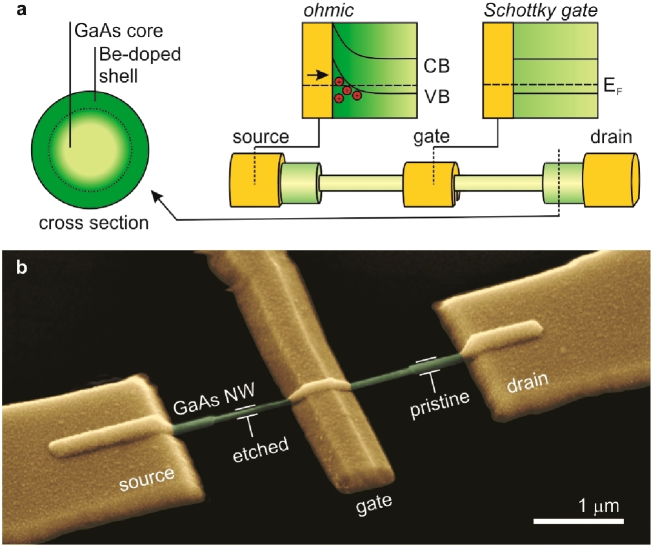
A controlled near-monolayer accuracy etch for GaAs nanowires Figure 1 shows a schematic of the -GaAs nanowire MESFET structure and a scanning electron micrograph of a completed device. The nanowire is grown as an undoped core with a heavily Be-doped shell (see Methods for full details), however, this does not mean the Be-dopants remain confined to the shell alone. Be has a high diffusion constant in GaAs, 37 which means significant amounts of the Be diffuse into the otherwise-undoped core. 38 The result is a roughly constant doping density in the shell and a monotonically decreasing doping density moving into the core; 38 for a much higher doping density than we use, this can result in a fully doped core. 39 This aspect of the doping profile is crucial to properly understanding our device. It also underpins our ability to make devices with high repeatability and yield given a well-engineered nanowire etch process. We leave the shell intact at the source and drain contacts as shown in Fig. 1 to minimise the contact resistance. The key is then to thin the nanowire and thereby reduce the doping level at the gate location just enough for the channel to become electrostatically gateable in the region where the gates are placed. This requires a careful balance – etch insufficiently and the gate either fails to function 30 and/or leaks current to the nanowire; etch too much and the on-resistance become undesirably high and the on-off ratio falls. 29 Note that it is vital that some doping remains in the etched region to counteract the GaAs surface-states, which pin the Fermi energy at mid-gap, and then provide the free holes required to achieve conduction through the etched channel segment. The gate-etch is thus administered completely ignoring the location of the core-shell boundary. Indeed, for our optimum devices below, we completely etch the shell and somewhat into the core.
We used a phosphoric acid etch H3PO4:H2O2:H2O, inspired by Mori and Watanabe’s work 40 on slow etching of GaAs wafers for microwave devices to obtain a highly-controllable nanowire gate-etch without deleterious effects. We made attempts with other etchants, e.g., sulfur-oleylamine, which has previously shown near-monolayer etch control for III-Vs 41, but only the phosphoric acid etchant proved compatible with other aspects of nanowire device fabrication (see Supplementary Information for further discussion). We note that a two-step digital etch process could also be applied; 42 it may provide more precision than our \ceH3PO4 etch but our nm etch depth may also make it a high time-cost option. With this in mind, one could suggest using a thinner shell and increasing the doping density to avoid loss in contact performance. The issue here is that this drives dopant diffusion into the core, 39 as discussed above, requiring a deeper gate-etch to achieve a functional doping level at the gated segment. This defeats the purpose of thinning the shell in the first place.
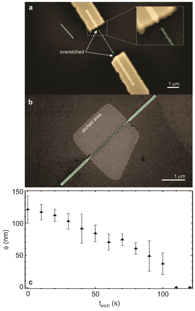
An important consideration when performing the gate-etch for a GaAs nanowire MESFET is the stage where the etch is performed. The simplest option is to pattern the source and drain contacts first and use these as a mask for a ‘self-aligned’ gate-etch 43. The outcome is shown in Fig. 2a, where the nanowire etches much faster local to the contact edges than near the middle, presumably due to metal-assisted etching 44. This is supported by the fact that the nanowire segment off to the left in Fig. 2a, which was also exposed to the etchant, is not as heavily etched. We avoided this problem by performing the etch prior to contact deposition, using EBL-patterned polymethylmethacrylate (PMMA) resist as the etch mask. This gives the more even gate-etch shown in Fig. 2b, and was the etch process used to obtain the device shown in Fig. 1b. The fact that the nanowire is sitting on a substrate may slightly reduce the etch rate at the bottom of the nanowire, which could produce a slight inhomogeneity in doping density on this side. We do not expect this effect to be substantial given the same issue did not adversely affect our earlier horizontal wrap-gate nanowire devices, 45, 46 where a similar wet-etch was administered, or appear to be detrimental to the performance of the devices made here. This issue would be eliminated entirely in the vertical orientation preferred for applications.
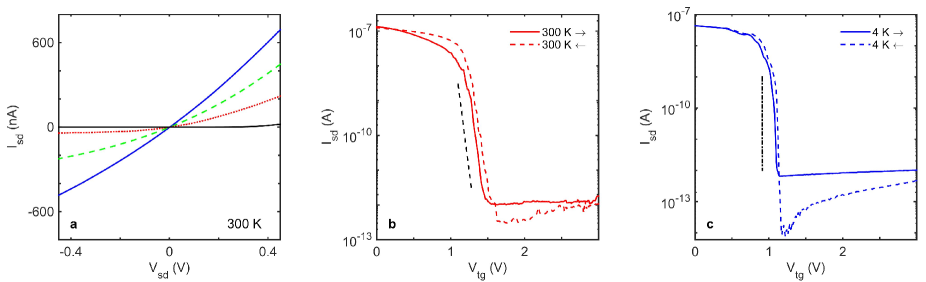
Figure 2c shows a plot of the etched segment diameter versus etch time for the phosphoric acid etch. The diameter was measured by post-etch scanning electron microscopy, with results averaged over separate nanowires for each . The etch is well controlled for s. At longer the nanowire becomes sufficiently thin that the etch acts anisotropically, producing breaks and substantial thickness variations. The long behaviour is not problematic since we only aim to slightly thin the nanowire and this requires significantly less than s. Some readers may note a slight gradient change to the linear trend in Fig. 2c at approximately s. Given a nominal shell thickness of nm and a typical etch rate of nm/s, this likely arises from the etch crossing the core-shell boundary.
Obtaining high-performance -GaAs nanowire MESFETs with controlled gate-segment etching The challenge in the fabrication is to identify the appropriate needed to optimise electrical performance. Optimum performance was obtained for s, yielding the electrical characteristics in Fig. 3. Figure 3a shows versus at four different top-gate voltages . The versus characteristic is relatively linear for V, with slope corresponding to an unbiased channel resistance k. The typical contact resistance at K for these nanowires is k 29. An increasingly positive results in reduced at a given , as expected for a -MESFET, without severe degradation in source-drain characteristics. Figure 3b shows versus at mV at K. We obtain remarkably strong gating with a sub-threshold swing of mV/dec at K. This is within of the room-temperature thermal limit of mV/dec, which is indicated by the black dashed line in Fig. 3b for comparison. The K data has on-off ratio , threshold voltage V and relatively low hysteresis; the up and down traces in Fig. 3b are separated by only mV in at A. We will comment further on normalised on-current, peak transconductance and field-effect mobility in our benchmarking comparison to other devices below.
Potential for studying hole-based quantum devices Our device architecture may also be useful for quantum device applications. A concern is that gate-etch might cause conduction to freeze-out before sufficiently low temperature for observing quantum effects is attained. To test this we repeated the versus characterisation after cooling to K, as shown in Fig. 3c. The on-resistance increases slightly to M consistent with the etched channel segment being non-metallic. Strong gating is retained but the sub-threshold swing of mV/dec is not as close to the respective thermal limit ( mV/dec at K – black dot-dashed line in Fig. 3c for comparison). This is a positive outcome for quantum device applications, as very steep gate response makes it harder to control/study quantum effects, e.g., 1D conductance quantization 47, 48, 49 and can increase noise as smaller gate voltage fluctuations give a stronger effect. The on-off ratio at K remains high () and the threshold voltage V shifts slightly closer to zero, consistent with reduced ionized dopant density due to freeze-out. The hysteresis is also improved significantly upon cooling. Optimisation of the gate-etch for quantum device applications will be subject of a separate study.
Comparison of performance with -GaSb nanowire MOSFETs The most notable competitor for our devices is the -GaSb nanowire MOSFET, which is the current device of choice for complementary architectures featuring III-V nanowires. We will make this comparison in two stages. First we will compare to horizontally-oriented single nanowire devices to make a direct ‘like-for-like’ performance comparison. We will then benchmark against more recently developed vertical nanowire array devices to consider prospects for scale-up and applications.
Dey et al. 20 previously reported single InAs/GaSb nanowire CMOS inverter oriented horizontally on a \ceSiO2-on-Si substrate. Their -GaSb MOSFET featured a nanowire with diameter nm and a gate length of nm, giving sub-threshold swing mV/dec, peak transconductance Sm, on-off ratio and a normalised on-resistance .mm at room temperature. Babadi et al. 21 improved to .mm by moderate doping with Zn coupled with a reduced gate length of nm. This improved the peak transconductance to Sm but also led to a significantly reduced sub-threshold swing of mV/dec. 21 A measurement of hole mobility was not provided in Dey et al. 20 but Babadi et al. 21 obtained a peak hole mobility of cm2/Vs.
Our sub-threshold swing of mV/dec significantly surpasses that obtained by Dey et al. and Babadi et al. above. Our peak transconductance Sm (normalised to channel circumference) is comparable with that obtained by Dey et al. 20 Our normalised on-resistance is .mm, which is lower than the device reported by Dey et al. but times higher than Babadi et al. 21 Improvement in our normalised on-resistance should be possible by reducing the channel length and/or increasing the shell doping density to improve the contact resistance and then compensating with increased gate-etch depth to maintain gate-performance. The hole mobility is challenging to calculate for our device due to the absence of an oxide, but we can provide a reasonable estimate. The gate insulator in our device is the depletion region at the GaAs surface arising from surface states. Casadei et al. 38 calculate the surface depletion width as a function of doping density for nanowire radii of nm and nm. They obtain a depletion width of nm for our acceptor density cm-3 with negligible radii dependence, i.e., the depletion width values as a function of radii converge at high . 38 To obtain the top-gate capacitance we use a coaxial-capacitor model and reduce the resulting capacitance by to account for the gate not covering the bottom of the nanowire where it sits on the substrate. Assuming the standard value for GaAs dielectric constant of and the measured gate-length of nm for the device with s, we obtain a gate capacitance of fF. This in turn gives a hole mobility of cm2/Vs. This is lower than the mobility obtained by Babadi et al. 21 from devices with less than a third of the gate-length and much lower on-resistance. More competitive mobilities are probably attainable for -GaAs MESFETs with some optimisation of our design.
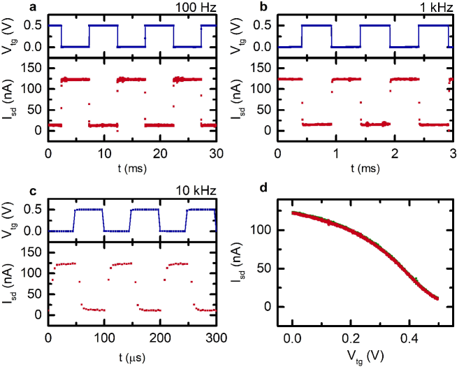
Figure 4 shows the frequency response of our s -GaAs MESFET. A square-wave top-gate voltage (blue trace/top panels) is applied at frequency Hz, kHz and kHz producing a square-wave source-drain current response (red trace/bottom panels) in each case. The fidelity for our device remains excellent up to kHz, where the leading edge begins to evolve a slight rounding. The high-frequency fidelity loss does not arise from the device acting as a low-pass filter – the fF gate capacitance estimated above combined with the k channel resistance gives a roll-off frequency of MHz. That said, radio-frequency operation is well-known to require careful capacitance management of the device and external circuit, and is commonly achieved for nanowire transistors by moving to vertical nanowire array structures. 7, 14 The fidelity loss we see likely arises from a mixture of instrument/circuit limitations and some gate-semiconductor interface effects; there will inevitably be some GaAs native oxide at the gate interface because the processing is not carried out in a fully oxygen-free environment. Charge trapping by oxide at gate interfaces is a well-known contributor to gate hysteresis in nanowire transistors. 32, 33, 34 The data in Fig. 3b indicates low hysteresis under dc operation; this performance is retained under ac conditions also. Figure 4d shows the device response to a triangle-wave signal between and V at Hz with the up-sweep to V data in green and the down-sweep data in red. Up and down sweeps are separated by a constant offset at higher frequencies (see Supplementary Fig. S3). We attribute this to a displacement current induced by the high gate-sweep rate. Regarding benchmarking of the frequency performance against -GaSb, Dey et al. 20 only present characteristics for their inverter and not their -GaSb MOSFET alone unfortunately. However, their inverter frequency response will be limited by the slowest component, which is inevitably the -GaSb MOSFET, giving some indication of its performance. The frequency performance of our -GaAs MESFET appears at least as good by this comparison – a more conclusive benchmarking would require a careful comparative study beyond the scope of the current work.
A notable aspect of our devices is the low gate leakage current despite the lack of an oxide gate insulator. We obtain gate leakage current pA over the entire operating range for devices with s. The gate-etch is essential to obtaining low gate leakage; for s we get nA at V (see Supplementary Fig. S4), as expected, since in this instance the heavy shell doping makes the metal gate electrode into an ohmic contact 50. For s we get yield of leakage-free gates albeit with reduced gate performance – Data obtained for s and s corresponding to Figs. 3 and 4 is presented in Supplementary Figs. to demonstrate this. At s we get excellent performance but the yield of leakage-free gates is only and drops sharply for shorter etch times. This makes s optimum on both performance and yield-to-performance measures, however, this would naturally vary for different growth conditions and require optimisation on a growth-batch basis. This performance compares very well to other single nanowire MESFETs, for example, Noborisaka et al. 36 report leakage currents between and pA for a -InGaAs device, Fortuna & Li 35 report pA to nA for a -GaAs device, and Liu et al. 51 report pA for a -\ceZn3P2 device.
Prospects for scale-up Development for practical applications tends to focus on vertical nanowire arrays over horizontal single nanowire devices for reasons of higher current carrying capacity, improved gate coupling and scalability, and capacitance management for high-frequency operation. 7, 9 A key aspect in vertical array devices is that the gate-length is no longer constrained by lithography and instead controlled by layer thicknesses during processing, facilitating scaling to sub- nm gate length. This pathway has already been taken for -GaSb, with the single horizontal nanowire devices of Dey et al. 20 and Babadi et al. 21 translated into vertical nanowire array structures by, e.g., Svensson et al. 22 and Jönsson et al. 23. The nanowire III-V CMOS on Si inverter structures by Jönsson et al. 23 represent the state-of-the-art in the field and feature a -GaSb device containing an array of nanowires with nm pitch, nm diameter and nm gate length. These transistors give sub-threshold swing mV/dec, normalised on-resistance .mm and peak transconductance Sm. The on-resistance and peak transconductance are superior, as one would expect for an array. Our sub-threshold swing is better, but we have to acknowledge that this metric is often compromised slightly in array structures by wire-to-wire variations. Benchmarking on ac operation is difficult because such data is limited for -GaSb array transistors. Svensson et al. 22 demonstrate ac operation of an inverter featuring -InAs and -GaSb vertical nanowire array transistors at kHz with good fidelity but report significant distortion at higher frequencies due to parasitic capacitance issues. These issues are more related to the vertical nanowire array layout than the nanowire channel itself; at this point the only comment we can make is that our -GaAs nanowire performance does not indicate that scale-up to arrays for high frequency operation would be obviously problematic.
Potential for complementary GaAs nanowire MESFET circuits Looking forwards, an interesting consideration is the scope for complementary circuits featuring only (In,Al)GaAs nanowire MESFETs, which would require an -channel device to complement the -GaAs design we present here. We see several alternatives. The first is a pure GaAs implementation. Fortuna and Li 35 reported a -GaAs nanowire MESFET featuring a nanowire grown epitaxially along the surface of a GaAs substrate. Their device gave strong electronic performance with sub-threshold swing mV/dec, on-off ratio and low contact resistance k. Noborisaka et al. 36 reported an -InGaAs nanowire MESFET with sub-threshold swing mV/dec, on-off ratio and low channel resistance k. More recently, Morkötter et al. 12 demonstrated a delta-doped GaAs-AlGaAs core-shell nanowire -MESFET with mV/dec, on-off ratio exceeding and k. With the latter, complementary circuits could be made on Si substrates using ‘pick and place’ micro-manipulation techniques. An exciting alternative would be to grow the GaAs nanowires directly on Si by template-assisted selective epitaxy 52, although a challenge here would be doping of separate GaAs nanowires to be deterministically or -type.
We demonstrated a -GaAs nanowire MESFET with strong electronic performance by taking a GaAs nanowire with an undoped core and heavily Be-doped shell and carefully etching the nanowire at the gate location to enable a Schottky-gate without compromising on contact resistance. We obtain a sub-threshold swing of mV/dec, within of the room-temperature thermal limit, on-off ratio , on-resistance k and typical contact resistance k. Accounting for nanowire diameter, we obtain a normalised on-resistance of .mm and peak transconductance of Sm. We estimate a field-effect hole mobility of cm2/Vs for our device. Our overall single MESFET performance is competitive with that obtained for single horizontal -GaSb nanowire MOSFETs, 20, 21 and suggests that scale-up to vertical nanowire transistor arrays may lead to devices that could potentially compete well with -GaSb vertical nanowire array transistors. 22, 23 Our -GaAs MESFETs show good square-wave fidelity for frequencies up to kHz, comparable to single horizontal -GaSb nanowire MOSFETs 20. The ability to eliminate the gate oxide in our device results in strong gating and reduced issues with charge-trapping effects, e.g., gate hysteresis. Our -GaAs MESFETs show strong potential for combination with high-performance -type (In,Al)GaAs MESFETs 36, 35, 12 towards nanowire complementary circuit applications, perhaps even ultimately integrated monolithically on Si using templated epitaxy techniques 52.
Methods
The GaAs nanowires were self-catalysed 53 and grown by molecular beam epitaxy on Si 38. The undoped core was grown at C using As4 and a V/III flux ratio of for min. The Be-doped shell was grown at C using As2 and a V/III ratio of for min. giving nanowires with shell acceptor density cm-3, diameter nm and length m. These nanowires are the highest doping density from earlier work on contacts to -GaAs nanowires 29. The nanowires are pure zincblende crystal phase but may have short wurtzite segments at the ends 27; these wurtzite segments will be buried under the source/drain contacts. Nanowires were dry-transferred to a pre-patterned HfO2/SiO2-coated -Si substrate for device fabrication. The heavily-doped substrate was used as a global back-gate for control studies. The source and drain contacts were defined by electron-beam lithography (EBL) and thermal evaporation of nm of Be:Au alloy (ACI alloys) and were not thermally annealed 29. The thin GaAs native oxide was removed at the contact interfaces by a s etch in HCl solution immediately prior to contact deposition. The / nm Ti/Au gate electrode was formed in a separate round of EBL and metal deposition. Electrical measurements were performed at temperature K in ambient atmosphere and at K by immersion in liquid helium. The source-drain current was measured using a Keithley 6517A electrometer for the dc measurements in Fig. 3 and using a Femto DLPCA-200 pre-amplifier connected to a National Instruments USB-6216 data acquisition system for the ac measurements in Fig. 4. Keithley K2410 voltage sources supplied the source-drain voltage , top-gate voltage and back-gate voltage (back-gate used in control studies only) for the dc measurements. In the ac measurements was instead supplied from a Stanford Research Systems DS345 signal generator.
Supporting Information. Additional fabrication details and electrical data, as well as a discussion of attempts with sulfur-oleylamine etchant. This material is available free of charge via the Internet at http://pubs.acs.org.
We thank D.J. Carrad for helpful discussions. This work was funded by the Australian Research Council (ARC) grants DP170102552 and DP170104024, the University of New South Wales, Danish National Research Foundation and the Innovation Fund Denmark. This work was performed in part using the NSW node of the Australian National Fabrication Facility (ANFF).
References
- 1 :
- 2 Chandrakasan, A.P., Sheng, S. and Brodersen, R.W., Low-power CMOS digital design. IEEE Journal of Solid-state Circuits 27, 473-484 (1992).
- 3 ITRS International Technology Working Groups. International Technology Roadmap for Semiconductors 2015 edition. Available at http://www.itrs.net (2015).
- 4 Lu, W. and Lieber, C.M., Nanoelectronics from the bottom up. Nature Materials 6, 841-850 (2007).
- 5 Barraud, S., Lapras, V., Previtali, B., Samson, M.P., Lacord, J., Martinie, S., Jaud, M.-A., Athanasiou, S., Triozon, F., Rozeau, O., Hartmann, J.M., Vizioz, C., Comboroure, C., Andrieu, F., Barbé, J.C., Vinet, M. and Ernst, T., Performance and design considerations for gate-all-around stacked-NanoWires FETs, Proceedings of the 2017 IEEE International Electron Devices Meeting (IEDM), San Francisco, CA, pp. 29.2.1-29.2.4, (2017).
- 6 Mertens, H., Ritzenthaler, R., Pena, V., Santoro, G., Kenis, K., Schulze, A., Litta, E.D., Chew, S.A., Devriendt, K., Chiarella, T., Demuynck, S., Yakimets, D., Jang, D., Spessot, A., Eneman, G., Dangol, A., Lagrain, P., Bender, H., Sun, S., Korolik, M., Kioussis, D., Kim, M., Bu, K.-H., Chen, S.C., Cogorno, M., Devrajan, J., Machillot, J., Yoshida, N., Kim, N., Barla, K., Mocuta, D. and Horiguchi, N., Vertically stacked gate-all-around Si nanowire transistors: Key Process Optimizations and Ring Oscillator Demonstration, Proceedings of the 2017 IEEE International Electron Devices Meeting (IEDM), San Francisco, CA, pp. 37.4.1-37.4.4, (2017).
- 7 Wernersson, L.-E., Thelander, C., Lind, E. and Samuelson, L., III-V nanowires – Extending a narrowing road. Proceedings of the IEEE 98, 2047-2060 (2010).
- 8 del Alamo, J.A., Nanometre-scale electronics with III-V compound semiconductors. Nature 479, 317-323 (2011).
- 9 Riel, H., Wernersson, L.-E., Hong, M. and del Alamo, J.A., III-V compound semiconductor transistors – from planar to nanowire structures. MRS Bulletin 39, 668-677 (2014).
- 10 del Alamo, J.A., Antoniadis, D.A., Lin, J., Lu, W., Vardi, A, and Zhao, X., Nanometer-scale III-V MOSFETs. J. Electron. Dev. Soc. 4, 205-214 (2016).
- 11 Tomioka, K., Yoshimura, M. and Fukui, T., A III-V nanowire channel on silicon for high-performance vertical transistors. Nature 488, 189-192 (2012).
- 12 Morkötter, S., Jeon, N., Rudolph, D., Loitsch, B., Spirkoska, D., Hoffmann, E., Döblinger, M., Matich, S., Finley, J.J., Lauhon, L.J., Abstreiter, G. and Koblmüller, G., Demonstration of confined electron gas and steep-slope behavior in delta-doped GaAs-AlGaAs core-shell nanowire transistors. Nano Letters 15, 3295-3302 (2015).
- 13 Schmid, H., Borg, M., Moselund, K., Cignac, L., Breslin, C.M., Bruley, J., Cutaia, D. and Riel, H., Template-assisted selective epitaxy of III-V nanoscale devices for co-planar heterogeneous integration with Si. Applied Physics Letters 106, 233101 (2015).
- 14 Johansson, S., Memisevic, E., Wernersson, L.-E. and Lind, E., High-frequency gate-all-around vertical InAs nanowire MOSFETs on Si substrates. IEEE Electron Device Letters 35, 518-520 (2014).
- 15 Sørensen, B.S., Aagesen, M., Sørensen, C.B., Lindelof, P.E., Martinez, K.L. and Nygård, J., Ambipolar transistor behavior in -doped InAs nanowires grown by molecular beam epitaxy. Applied Physics Letters 92, 012119 (2008).
- 16 Storm, K., Nylund, G., Börgstrom, M.T., Wallentin, J., Fasth, C., Thelander, C. and Samuelson, L., Gate-induced Fermi level tuing in InP nanowires at efficiency close to the thermal limit. Nano Letters 11, 1127-1130 (2011).
- 17 Nilsson, H.A., Caroff, P., Thelander, C., Lind, E., Karlström, O. and Wernersson, L.-E., Temperature dependent properties of InSb and InAs nanowire field-effect transistors. Applied Physics Letters 96, 153505 (2010).
- 18 Ling, C.C., Lui, M.K., Ma, S.K., Chen, X.D., Fung, S. and Beling, C.D., Nature of the acceptor responsible for -type conduction in liquid encapsulated Czochralski-grown undoped gallium antimonide. Applied Physics Letters 85, 384-386 (2004).
- 19 Virkkala, V., Havu, V., Tuomisto, F. and Puska, M.J., Native point defect energetics in GaSb: Enabling -type conductivity in undoped GaSb. Physical Review B 86, 144101 (2012).
- 20 Dey, A.W., Svensson, J., Borg, B.M., Ek, M. and Wernersson, L.-E., Single InAs/GaSb nanowire low-power CMOS inverter. Nano Letters 12, 5593-5597 (2012).
- 21 Babadi, A.S., Svensson, J., Lind, E. and Wernersson, L.-E., Impact of doping and diameter on the electrical properties of GaSb nanowires. Applied Physics Letters 110, 053502 (2017).
- 22 Svensson, J., Dey, A.W., Jacobsson, D. and Wernersson, L.-E., III-V nanowire complementary metal-oxide semiconductor transistors monolithically integrated on Si. Nano Letters 15, 7898-7904 (2015).
- 23 Jönsson, A., Svensson, J. and Wernersson, L.-E., A self-aligned gate-last process applied to All-III-V CMOS on Si. IEEE Electron Dev. Lett. 39, 935-938 (2018).
- 24 Borg, B.M. and Wernersson, L.-E., Synthesis and properties of antimonide nanowires. Nanotechnology 24, 202001 (2013).
- 25 Yang, Z.-X., Yip, S., Li, D., Han, N., Dong, G., Liang, X., Shu, L., Hung, T.F., Mo, X. and Ho, J.C., Approaching the hole mobility limit of GaSb nanowires. ACS Nano 9, 9268-9275 (2015).
- 26 Fontcuberta i Morral, A., Colombo, C., Abstreiter, G., Arbiol, J. and Morante, J.R., Nucleation mechanism of gallium-assisted molecular beam epitaxy growth of gallium arsenide nanowires. Appl. Phys. Lett. 92 063112 (2008).
- 27 Krogstrup, P., Popovitz-Biro, R., Johnson, E., Madsen, M., Nygård, J. and Shtrikman, H., Structural phase control in self-catalyzed growth of GaAs nanowires on silicon(111). Nano Letters 10, 4475-4482 (2010).
- 28 Waldrop, J.R., Schottky-barrier height of ideal metal contacts to GaAs. Appl. Phys. Lett. 44, 1002-1004 (1984).
- 29 Ullah, A.R., Gluschke, J.G., Krogstrup, P., Sørensen, C.B., Nygård, J. and Micolich, A.P., Towards low-dimensional hole systems in Be-doped GaAs nanowires. Nanotechnology 28, 134005 (2017).
- 30 Ullah, A.R., Carrad, D.J., Krogstrup, P., Nygård, J. and Micolich, A.P., Near-thermal limit gating in heavily doped III-V semiconductor nanowires using polymer electrolytes. Phys. Rev. Materials 2, 025601 (2018).
- 31 Carrad, D.J., Mostert, A.B., Ullah, A.R., Burke, A.M., Joyce, H.J., Tan, H.H., Jagadish, C., Krogstrup, P., Nygård, J., Meredith, P. and Micolich, A.P., Hybrid nanowire ion-to-electron transducers for integrated bioelectronic circuitry. Nano Lett. 17, 827-833 (2017).
- 32 Dayeh, S.A., Soci, C., Yu, P.K.L., Yu, E.T. and Wang, D., Influence of surface states on the extraction of transport parameters from InAs nanowire field effect transistors. Appl. Phys. Lett. 90, 162112 (2007).
- 33 Roddaro, S., Nilsson, K., Astromskas, G., Samuelson, L., Wernersson, L.-E., Karlström, O. and Wacker, A., InAs nanowire metal-oxide-semiconductor capacitors. Appl. Phys. Lett. 92, 253509 (2008).
- 34 Holloway, G.W., Song, Y., Haapamaki, C.M., LaPierre, R.R. and Baugh, J., Trapped charge dynamics in InAs nanowires. J. Appl. Phys. 113, 024511 (2013).
- 35 Fortuna, S.A. and Li, X., GaAs MESFET with a high-mobility self-assembled planar nanowire channel. IEEE Electron Device Letters 30, 593-595 (2009).
- 36 Noborisaka, J., Sato, T., Motohisa, J., Hara, S., Tomioka, K. and Fukui, T., Electrical characteristics of InGaAs nanowire-top-gate field-effect transistors by selective-area metal organic vapor phase epitaxy. Jpn. J. Appl. Phys. 46, 7562-7568 (2007).
- 37 Ilegems, M., Beryllium doping and diffusion in molecular-beam epitaxy of GaAs and AlxGa1-xAs. J. Appl. Phys. 48, 1278-1287 (1977).
- 38 Casadei, A., Krogstrup, P., Heiss, M., Röhr, J.A., Colombo, C., Ruelle, T., Upadhyay, S., Sørensen, C.B., Nygård, J. and Fontcuberta i Morral, A., Doping incorporation paths in catalyst-free Be-doped GaAs nanowires. Applied Physics Letters 102, 013117 (2013).
- 39 Koren, E., Hyun, J.K. Givan, U., Hemesath, E.R., Lauhon, L.J. and Rosenwaks, Y., Obtaining uniform dopant distributions in VLS-grown Si nanowires. Nano Lett. 11, 183-187 (2011).
- 40 Mori, Y. and Watanabe, N., A new etching solution system, H3PO4-H2O2-H2O, for GaAs and its kinetics. J. Electrochem. Soc. 125, 1510-1514 (1978).
- 41 Naureen, S., Shahid, N., Sanatinia, R. and Anand, S., Top-down fabrication of high quality III-V nanostructures by monolayer controlled sculpting and simultaneous passivation. Adv. Funct. Mater. 23, 1620-1627 (2013).
- 42 Lu, W., Zhao, X., Choi, D., El Kazzi, S. and del Alamo, J., Alcohol-based digital etch for III-V vertical nanowires with sub- nm diameter. IEEE Electron Device Letters 38, 548-551 (2017).
- 43 Kane, B.E., Pfeiffer, L.N., West, K.W. and Harnett, C.K., Variable density high mobility two-dimensional electron and hole gases in a gated GaAs/AlxGa1-xAs heterostructure. Appl. Phys. Lett. 63, 2132-2134 (1993).
- 44 DeJarld, M., Shin, J.C., Chern, W., Chanda, D., Balasundaram, K., Rogers, J.A. and Li, X., Formation of high aspect ratio GaAs nanostructures with metal-assisted chemical etching. Nano Letters 11, 5259-5263 (2011).
- 45 Storm, K., Nylund, G., Samuelson, L. and Micolich, A.P., Realizing lateral wrap-gate nanowire FETs: Controlling gate length with chemistry rather than lithography. Nano Lett. 12, 1-6 (2012).
- 46 Burke, A.M., Carrad, D.J., Gluschke, J.G., Storm, K., Fahlvik Svensson, S., Linke, H., Samuelson, L. and Micolich, A.P., InAs nanowire transistors with multiple, independent wrap-gate segments. Nano Lett. 15, 2836-2843 (2015).
- 47 van Weperen, I., Plissard, S.R., Bakkers, E.P.A.M., Frolov, S.M. and Kouwenhoven, L.P., Quantized conductance in an InSb nanowire. Nano Lett. 13, 387-391 (2013).
- 48 Heedt, S., Prost, W., Schubert, J., Grützmacher, D. and Schäpers, Th., Ballistic transport and exchange interaction in InAs nanowire quantum point contacts. Nano Lett. 16, 3116-3123 (2016).
- 49 Irber, D.M., Seidl, J., Carrad, D.J., Becker, J., Jeon, N., Loitsch, B., Winnerl, J., Matich, S., Döblinger, M., Tang, Y., Morkötter, S., Abstreiter, G., Finley, J.J., Grayson, M, Lauhon, L.J. and Köblmuller, G., Quantum transport and sub-band structure of modulation-doped GaAs/AlAs core-superlattice nanowires. Nano Lett. 17, 4886-4893 (2017).
- 50 Baca, A.G., Ren, F., Zolper, J.C., Briggs, R.D. and Pearton, S.J., A survey of ohmic contacts to III-V compound semiconductors. Thin Solid Films 308-309, 599-606 (1997).
- 51 Liu, C., Dai, L., Ma, R.M., Yang, W.Q. and Qin, G.G., -\ceZn3P2 single nanowire metal-semiconductor field-effect transistors. J. Appl. Phys. 104, 034302 (2008).
- 52 Knoedler, M., Bologna, N., Schmid, H., Borg, M., Moselund, K.E., Wirths, S., Rossell, M.D. and Riel, H., Observation of twin-free GaAs nanowire growth using template-assisted selective epitaxy. Cryst. Growth Des. 17, 6297-6302 (2017).
- 53 Colombo, C., Spirkoska, D., Frimmer, M., Abstreiter, G. and Fontcuberta i Morral, A., Ga-assisted catalyst-free growth mechanism of GaAs nanowires by molecular beam epitaxy. Physical Review B 77, 155326 (2008).