Absence of a giant spin Hall effect in plasma-hydrogenated graphene
Abstract
The weak spin-orbit interaction in graphene was predicted to be increased, e.g., by hydrogenation. This should result in a sizable spin Hall effect (SHE). We employ two different methods to examine the spin Hall effect in weakly hydrogenated graphene. For hydrogenation we expose graphene to a hydrogen plasma and use Raman spectroscopy to characterize this method. We then investigate the SHE of hydrogenated graphene in the H-bar method and by direct measurements of the inverse SHE. Although a large nonlocal resistance can be observed in the H-bar structure, comparison with the results of the other method indicate that this nonlocal resistance is caused by a non-spin-related origin.
I Introduction
Covalently bonded hydrogen was predicted to significantly increase the spin-orbit coupling (SOC) of graphene by Castro Neto and GuineaCastro Neto and Guinea (2009). However, experimental results on this were conflicting. Balakrishnan et al. reported a high nonlocal resistance in weakly hydrogenated graphene in the so called H-bar structureBalakrishnan et al. (2013). They further observed an oscillatory behavior of this nonlocal resistance with an in-plane magnetic field and therefore attributed this effect to the SHE with a spin Hall angle of around . A high nonlocal resistance in similar samples was also observed by Kaverzin and van WeesKaverzin and van Wees (2015). However they obtained an unrealistically high value for the spin Hall angle of and could not observe any effect of an in-plane magnetic field on this nonlocal resistance. They therefore argue that this nonlocal signal has a non spin related origin.
Here, we perform different types of experiments to solve this controversy. For hydrogenation we expose graphene to a hydrogen plasma which has several advantages over the hydrogenation method by exposing hydrogen silsesquioxane (HSQ) to an electron beam, employed in Refs. Balakrishnan et al., 2013; Kaverzin and van Wees, 2015. We use Raman spectroscopy to characterize graphene exposed to hydrogen or deuterium to verify that the created defects by this method are indeed bonded hydrogen atoms. Then we perform non-local measurements in the so-called H-bar geometry in graphene that was hydrogenated by this method. Further, we employ electrical spin injection into hydrogenated graphene to perform spin transport measurements as well as measurements of the inverse spin Hall effect. Our results show that the large nonlocal signal in hydrogenated graphene is not related to the spin Hall effect.
II Plasma hydrogenation of graphene
Due to limitations of the HSQ-based hydrogenation procedure, which we describe in more detail below, we explore hydrogenation by exposing graphene to a hydrogen plasma in a reactive ion etching chamber (RIE). Following the recipe developed by Wojtaszek et al.Wojtaszek et al. (2011), exfoliated graphene was exposed to hydrogen plasma of pressure mTorr, 30 sccm gas flow and 2 W power. The relatively low power leads to a low acceleration bias voltage of V, which reduces the creation of lattice defects. The samples were then investigated by Raman spectroscopy.
Fig. 1 (a) shows Raman spectra of samples with different plasma exposure time.
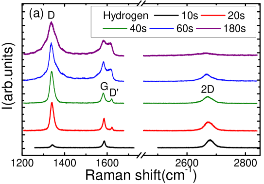
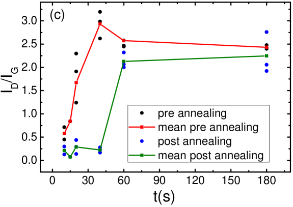
With increasing exposure time both a D-peak and a D′-peak arise, which indicate the presence of defects. For higher exposure times a decrease of the 2D-peak intensity can be observed which indicates an alteration of the electronic band structure. As can be seen in the red curve in Fig. 1 (c) the ratio between the D and G-peak intensities increases with exposure time up to a value around for an exposure time of s and decreases for longer exposure times. For low defect densities the ratio between D and G-peak intensities is proportional to the defect densityCancado et al. (2011):
| (1) |
with nm (given in nm in Eq. (1)) being the excitation wavelength. reaches its maximum when the average distance between defects becomes comparable to the distance an e-h pair travels in its lifetime, given by with being the D-peak frequencyCancado et al. (2011). At higher defect densities the D-peak becomes broader and its intensity decreases. Further, at high defect densities the graphene band structure is altered by the defects, which reduces possible transitionsFerrari (2007). Since the 2D peak is double resonant it is more sensitive to this alteration than the D- and G-peaks and therefore a reduction of the 2D-peak intensity with increasing exposure time can be observed in Fig. 1(a).
The green curve of Fig. 1(c) shows for the same samples after annealing in vacuum at 320 C for 1 h. For low plasma exposure times s annealing almost fully removes the defects. Since this temperature is too low to heal vacanciesZion et al. (2017) in graphene, this behavior indicates that for these low exposure times the observed defects are bonded hydrogen atoms. For s the defects could not be removed by annealing. Therefore the occurrence of lattice defects for higher plasma exposure times is likely. Possible explanations for this might be heating of the samples during the exposure process or etching of carbon atoms by the formation of CH2 after saturation of the hydrogen coverage of grapheneLuo et al. (2009).
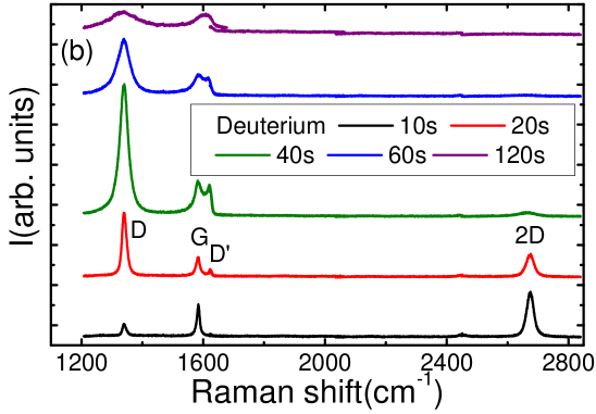
To further determine the type of the observed defects the same experiment was performed with deuterium instead of hydrogen. Fig. 1(b) shows Raman spectra for different exposure times. In comparison to Fig. 1(a) deuterium seems to induce slightly more defects than hydrogen as can be seen by the rapid decrease of 2D-peak intensity in Fig. 1(b). One explanation for this could be a higher reactivity of deuterium, due to a slightly increased binding energyParis et al. (2013). Another explanation is that the deuterium atoms are more likely to create lattice defects due to their higher mass.
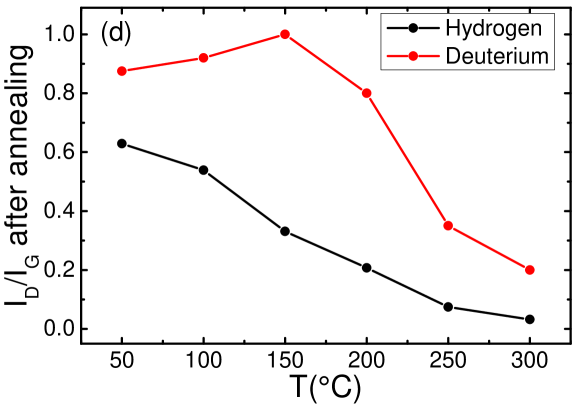
Samples exposed to either hydrogen or deuterium with an exposure time of s were annealed for 1 h in vacuum at different temperatures. Fig. 1(d) shows the relative ratio divided by its value before annealing. Surprisingly the bonded deuterium (red dots in Fig. 1(d)) is more stable with temperature than the hydrogen (black dots in Fig. 1(d)). A similar behavior has been observed for hydrogen and deuterium on graphiteZecho et al. (2002). This can be explained by a slightly increased binding energy of deuterium due to zero-point energy effectsParis et al. (2013) and a lower attempt frequency due to the higher mass of deuterium compared to hydrogen, hindering desorption Zecho et al. (2002). The fact that a different desorption behavior was found for hydrogen and deuterium is a clear indication that the defects created by this method are really bonded hydrogen since there should be no difference for other defect types.
Concerning the HSQ-based hydrogenation method employed in Refs. Balakrishnan et al., 2013; Kaverzin and van Wees, 2015; Ryu et al., 2008 we note several difficulties. First, the HSQ film cannot be removed after exposure without destroying the underlying graphene sheet. Therefore, hydrogenation can only be done as a last step of the sample fabrication. Since resist residues from previous steps proved to prevent efficient hydrogenation, it is expected that the hydrogen coverage produced by this method is not homogeneous. Second, a high p-type doping was always observed in samples produced by this method both in our measurements 111see supplemental material as well as in the measurements by Kaverzin and van Wees Kaverzin and van Wees (2015). This is problematic since the occurrence of the SHE is only expected close to the charge neutrality point (CNP) Ferreira et al. (2014), which in these samples is often not accessible due to the high doping. Third, it is not entirely clear that the defects produced by this method are really bonded hydrogen since the Raman measurements are not sensitive to the defect type. Therefore, in our experiments, we resort to plasma hydrogenation.
III Nonlocal resistance in hydrogenated graphene
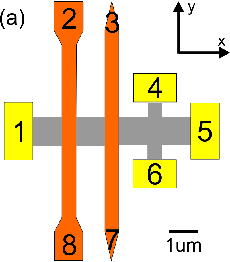
Using plasma hydrogenation a Hall-bar sample was fabricated. First, exfoliated graphene was exposed to hydrogen plasma for 20 s as described in the previous section. Afterwards, oxygen plasma was used to etch the graphene into a Hall bar and 0.5 nm Cr + 60 nm Au were deposited for contacts. A schematic picture of the sample structure is displayed in the inset of Fig. 2.
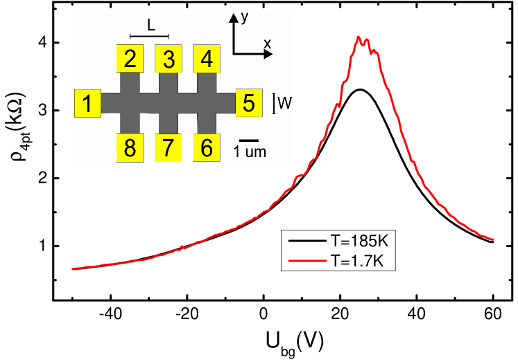
Raman measurements of this sample reveal . Using Eq. 1 and assuming that the defect density equals the hydrogen atom density, we extract a coverage of 0.0025%. This value is much lower than in the previous section for the same exposure time since several lithography steps and therefore resist bake-out steps were necessary after the hydrogenation process. However, employing hydrogenation as a first step in the sample fabrication process was preferred over using it as a last step since it is expected that resist residues lead to an inhomogeneous hydrogen coverage of the sample.
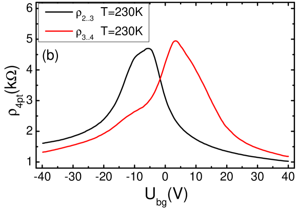
Back gate sweeps of the 4-point resistivity of this sample at temperatures K (black curve) and K (red curve) are depicted in Fig. 2. In this sample a p-type doping with V and mobilities of cmVs /( cmVs) for the hole side and cmVs ( cmVs) for the electron side at K ( K) were observed.
For obtaining the nonlocal resistance a current was applied between contacts 2 and 8 in the inset of Fig. 2 and a voltage is measured between contacts 3 and 7 (Fig. 3(a)) and between contacts 4 and 6 (Fig. 3(b)).
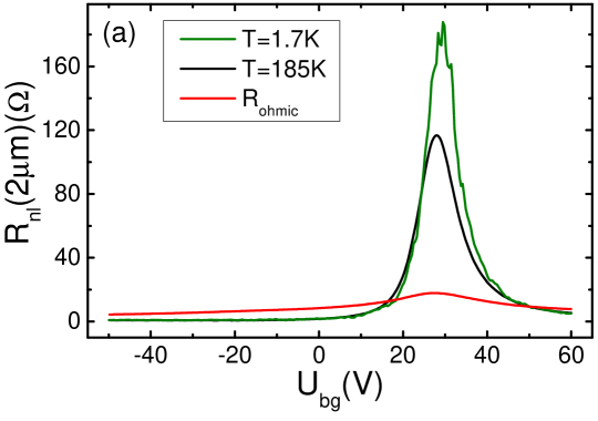
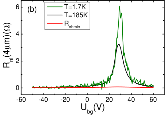
Decreasing the temperature from K (black curves in Fig. 3(a) and (b)) to K (green curves in Fig. 3(a) and (b)) increases the nonlocal resistance close to the charge neutrality point. The red curves depict the expected ohmic contribution given by , with being the 2-point resistance between contacts 2 and 8 and a geometry factor determined by a finite element simulation done with COMSOL. As can be seen in Fig. 3(a) and (b), close to the charge neutrality point the measured nonlocal resistances far exceeds the expected ohmic contribution.
As argued by Balakrishnan et al.Balakrishnan et al. (2013) this nonlocal resistance might be caused by an interplay between direct and inverse spin Hall effect. Then the nonlocal resistance as a function of distance to the current path is given byAbanin et al. (2009):
| (2) |
with the sheet resistivity , the sample width and the spin diffusion length . By comparing at the two different distances in Fig. 3(a) and (b) can be calculated to be in the range of nm. With this the spin Hall angle close to the charge neutrality point can be calculated to be for K and for K. These unrealistically high values are similar to the one reported by Kaverzin and van WeesKaverzin and van Wees (2015).
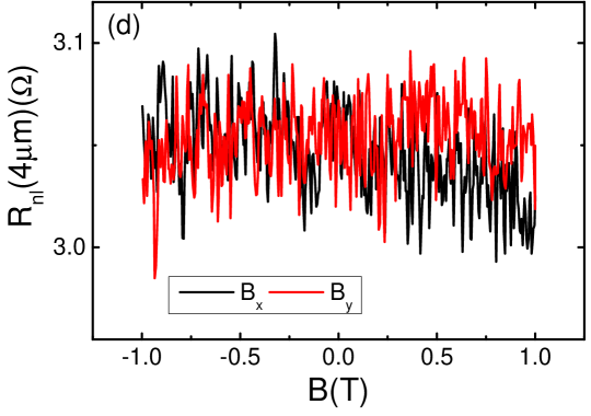
Further, in case that the large nonlocal resistance is caused by the spin Hall effect, should be sensitive to an in-plane magnetic field, due to Larmor precession of the spins. Therefore, an oscillatory behavior of is expected to followAbanin et al. (2009):
| (3) |
with being the Larmor frequency.
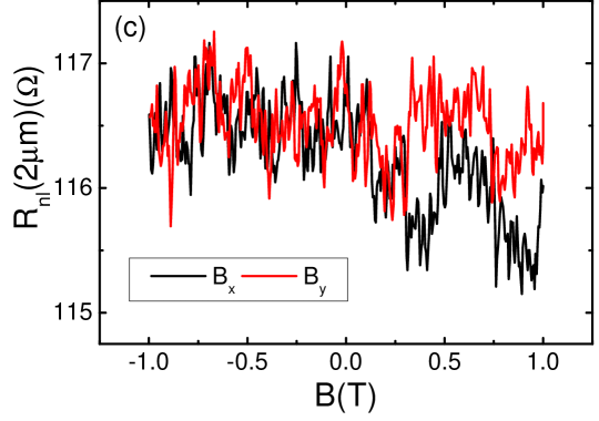
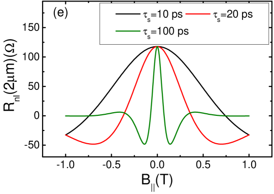
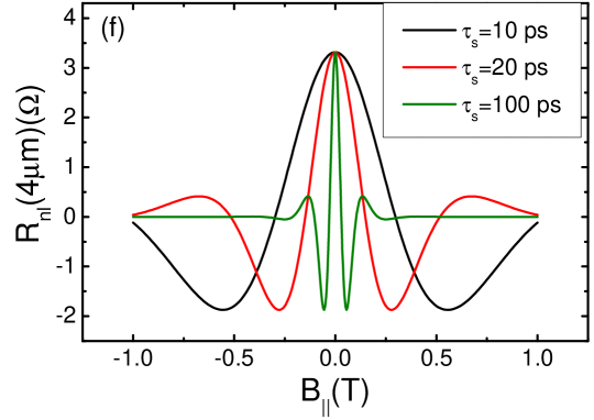
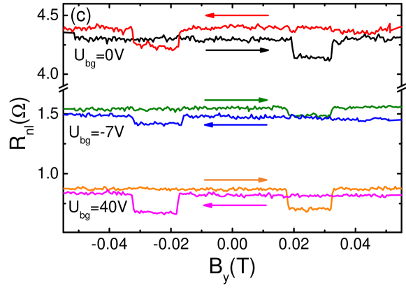
Fig. 3(c) and (d) show the influence of a magnetic field in both in-plane directions (black and red curves) on for two different distances from the current path. As can be seen, no significant change of with can be observed. This is in disagreement with the expected behavior given by Eq. 3, which is depicted in Fig. 3(e) and (f) for different values of in a realistic range, since a lower bound of ps could be established due to the absence of a weak antilocalization peakNote (1). As indicated here, a significant dependence of on should be visible.
IV Inverse spin Hall effect in hydrogenated graphene
Due to the difficulties arising from measuring the spin Hall effect in the H-bar geometry a more direct way for observing this effect is desirable. One way to examine the inverse spin Hall effect electrically was explored by Valenzuela and TinkhamValenzuela and Tinkham (2006) in aluminum wires. For this they employed electrical spin injection to create a spin current through the wire and measured a resulting nonlocal voltage across a Hall bar.
To employ this method in hydrogenated graphene the sample shown schematically in Fig. 4(a) was fabricated.
First, exfoliated graphene was exposed to hydrogen plasma for 20 seconds. Spin injection contacts consisting of 1.2 nm MgO, acting as a tunnel barrier, 50 nm Co and 10 nm Au were deposited (orange stripes in Fig. 4(a)). Afterwards 0.5 nm Cr +80 nm Au were deposited for contacts. As a last step oxygen plasma was employed to etch the sample.
Fig. 4(b) shows back gate sweeps of this sample, where a current was applied between contacts 1 and 5 and the voltage was taken between contacts 2 and 3 (black curve in Fig. 4(b)) and between contacts 3 and 4 (red curve in Fig. 4(b)). As can be seen the position of the charge neutrality point differs for the two areas. This can be caused by different doping of the areas either by the ferromagnetic contacts or by a difference in hydrogen coverage between the area underneath the stripes and the rest of the sample. Mobilities of cm2/Vs for the hole side and cm2/Vs for the electron side could be observed in this sample.
Further, nonlocal spin injection measurements were performed to examine whether spin injection is possible with these contactsJohnson and Silsbee (1985). Fig. 4(c) shows nonlocal spin-valve measurements at different back gate voltages. Here a current is applied between contacts 3 and 5 in Fig. 4(a) and a nonlocal voltage is measured between contacts 2 and 1. The magnetization of the ferromagnetic stripes is first aligned by a magnetic field in stripe direction of T. Then the magnetic field is swept in the opposite direction. Due to their different shape the two ferromagnet stripes have a different coercive field. As can be seen in Fig. 4(c) a clear difference between parallel and antiparallel alignment of the stripe magnetizations can be observed over the whole back gate range.
Applying an out-of plane magnetic field to this setup leads to precession of the spins around that field. The out-of plane magnetic field dependence is depicted in Fig. 5.
Here, a parabolic background that can be caused by a charge current contribution in the nonlocal path by the presence of pinholes in the tunnel barriersVolmer et al. (2015) was subtracted. In the low magnetic field range the nonlocal resistance follows the expected behavior of the Hanle-effectFabian et al. (2007):
| (4) |
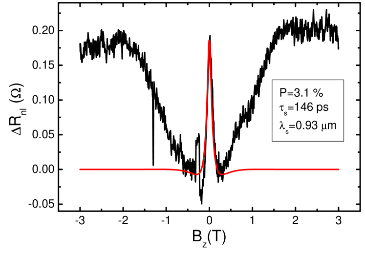
Fitting the data in the low magnetic field range (red curve in Fig. 5) reveals a spin injection efficiency of . The injection efficiency is much lower than what is typically observed with these kind of tunnel barriers in pristine graphene. This can be caused by an enhanced island growth of the MgO tunnel barrier due to the attached hydrogen and therefore an increase of pinholes in the barrier, resulting in a relatively low contact resistance of km2. Another explanation might be increased spin relaxation in the barrier due to the hydrogen atoms. It has to be noted that fabricating spin selective contacts in graphene that was hydrogenated by this method proved to be difficult in general.
Further, the extracted spin lifetime of ps is much smaller than what was observed in pristine graphene with tunneling contacts produced by the same methodRinger et al. (2018).This is in contrast to the findings of Wojtaszek et al. who observed an increase in spin lifetime after treating pristine graphene with hydrogen plasmaWojtaszek et al. (2013). This small value for the spin lifetime can be caused by either an increased contact-induced spin relaxation due to an increase in the number of pinholesVolmer et al. (2013) or due to increased spin relaxation by the presence of hydrogen atoms acting as magnetic impuritiesKochan et al. (2014). However, is still large enough that a clear oscillation of the nonlocal resistance in the H-bar geometry should be visible as shown by Fig. 3(e) and (f).
At higher magnetic fields the stripe magnetization is rotating into the out-of plane directions. Therefore the polarization of the injected spins has an out-of plane component that does not precess around the external field. The nonlocal resistance saturates around a magnetic field of T. This value coincides with the field at which the magnetization direction is completely rotated into the out-of plane direction, determined by anisotropic magnetoresistance measurementsNote (1).
Contrary to similar measurements performed by Tombros et al. in pristine grapheneTombros et al. (2008) no difference between the zero magnetic field value and the saturation value of the nonlocal resistance could be observed.
This indicates isotropic spin relaxation, consistent with the expected dominating spin relaxation mechanisms of contact-induced spin relaxation and spin relaxation due to spin-flip scattering at the absorbed hydrogen atoms. Both mechanisms result in isotropic spin relaxation.
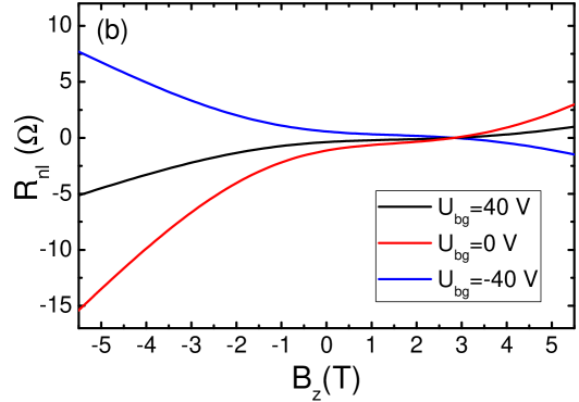
For measurement of the inverse spin Hall effect a current was applied between contacts 3 and 1 in Fig. 4(a) and a nonlocal voltage was measured between contacts 4 and 6. Without an external magnetic field the stripe magnetization is in the in-plane direction. Therefore no nonlocal voltage due to an inverse spin Hall effect is expected. Applying an out-of plane magnetic field results in a rotation of the stripe magnetization towards the out-of plane direction. The resulting out-of plane component of the spin polarization then leads to a nonlocal voltage that is expected to followValenzuela and Tinkham (2006):
| (5) |
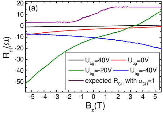
with being the projection of the stripe magnetization on the -axis. With Eq. 4 a saturation of the nonlocal resistance at T with is expected. The expected resulting with is depicted by the purple curve in Fig. 6(a). For this the angular dependence of the magnetization direction was extracted from Fig. 5Valenzuela and Tinkham (2006) and an offset was added for clarity.
The observed nonlocal resistance in this geometry for different back gate voltages is shown in Fig. 6(a). Here a large magnetic field dependent nonlocal resistance can be seen. However, no saturation of this nonlocal resistance for T was observed. The magnetic field dependence of the nonlocal resistance is therefore unlikely to be caused by the spin Hall effect.
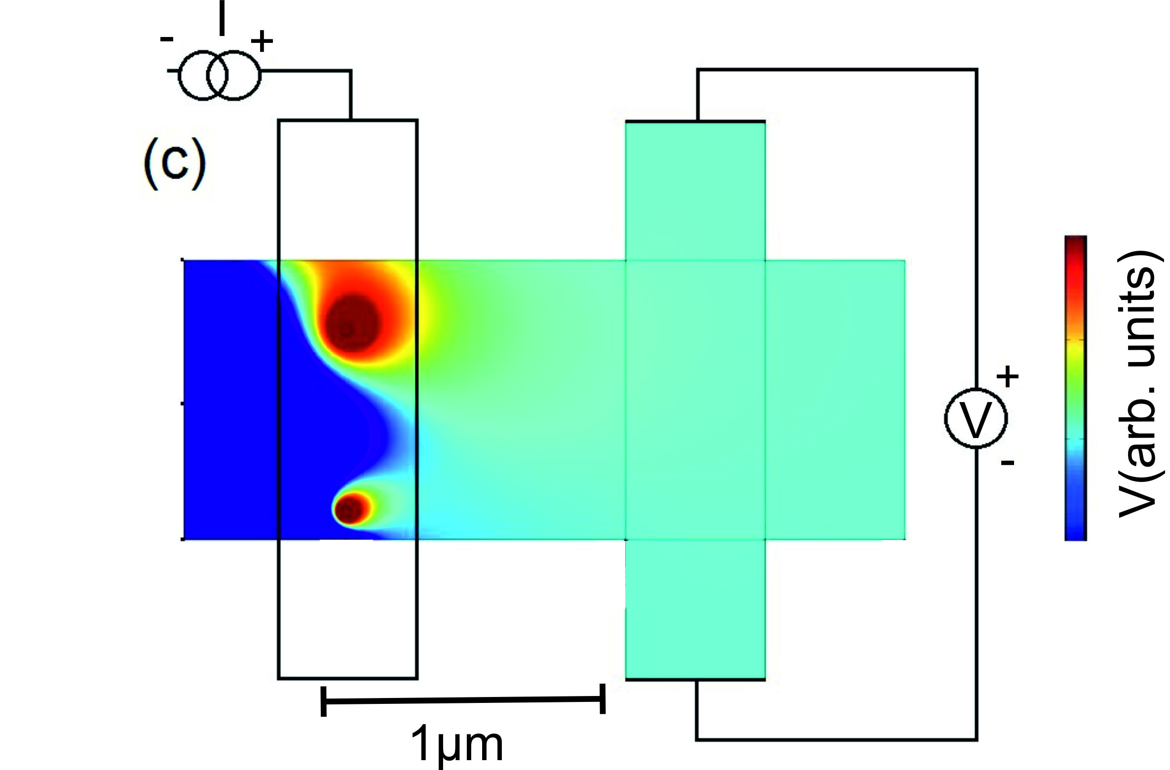
To determine the origin of this effect a finite element simulation done with COMSOL was performed. For this the potential distribution in the presence of two pinholes in the tunnel barrier was calculated (similar to the calculations in Ref. Volmer et al., 2015) as shown in Fig. 6(c). The resulting magnetic field dependence for different charge carrier concentrations shown in Fig. 6(b) is comparable to the nonlocal resistance in Fig. 6(a). Therefore it is likely that the observed magnetic field dependence of the nonlocal resistance is caused by a charge current effect due to the presence of pinholes.
This effect can mask a potential inverse spin Hall effect signal. However, the large spin Hall angle of resulting from the spin Hall interpretation of the H-bar geometry should still be observable close to the charge neutrality point V of the areas that are not covered by the ferromagnetic stripes.
V Spin Hall angle - an estimation of order of magnitude
In this section we provide a theoretical estimate of the upper bound of the spin Hall angle that conventionally expresses a rate conversion of the charge to the transverse spin-current in the presence of SOC. To model hydrogen chemisorption, we employ the tight-binding Hamiltonian inspired by first-principle calculations proposed in Ref. Gmitra et al., 2013. Plain graphene is described by the conventional nearest-neighbor Hamiltonian , and the hydrogen-induced perturbation including a locally enhanced SOC by Hamiltonian , see Refs. Gmitra et al., 2013; Kochan et al., 2017. Related transport characteristics are estimated on the methodology developed in Refs. Ferreira et al., 2014; Bundesmann et al., 2015. Particularly, for a given scattering process where an electron with the incident direction and spin, , elastically scatters to an outgoing state , we calculate the corresponding differential cross-section that depends also on the energy of the incident electron. Knowing we know spatial probability distributions of electrons with flipped or conserved spin depending on the relative angle . Elastic scattering governed by affects momentum relaxation due to resonances near the Dirac pointWehling et al. (2010); Irmer et al. (2018), and also spin relaxation due to locally enhanced SOCBundesmann et al. (2015). Despite the fact that hydrogen is predicted to induce also an unpaired magnetic momentYazyev and Helm (2007), which can serve as another spin relaxation channelKochan et al. (2014), we restrict our estimates of just to the local SOC interactions.
Assuming a spin polarized beam of, say, spin-up electrons with the incident energy , the upper bound of the spin Hall angle reads:
| (6) |
where the angle brackets represent averaging over all incoming directions . The calculation was performed for one hydrogen atom in a supercell containing 16120 carbon atoms, i.e. a hydrogen concentration of 0.0062 %. Fig. 7 displays as function of Fermi energy. The obtained values are in magnitude comparable with, e.g., those of Ferreira et al. Ferreira et al. (2014), but differ from the experimental data fitted by Eq. 2.

VI Discussion
The background effect observed in Fig. 6 could mask the relatively small spin Hall angle resulting from the theoretical estimation in Fig. 7. However, the high value of following from the SHE interpretation of the nonlocal resistance in Fig. 3(a) and (b) should still be observable. Further, this unusually high spin Hall angle as well as the absence of an oscillatory behavior of with an in-plane magnetic field support the findings of Kaverzin and van WeesKaverzin and van Wees (2015). These results suggest that the large nonlocal resistance observed in Fig. 3(a) and (b) is caused by a non spin-related mechanism.
Large nonlocal resistances in the H-bar structure were also observed in graphene decorated with heavy atomsWang et al. (2015), hBN/graphene heterostructuresGorbachev et al. (2014) and in graphene structured with an antidot arrayPan et al. (2017). These were attributed to the occurrence of a valley-Hall effectWang et al. (2015); Gorbachev et al. (2014), a nonzero Berry curvature, due to the presence of a band gapPan et al. (2017) and transport through evanescent wavesVan Tuan et al. (2016); Tworzydło et al. (2006). However none of these effects can sufficiently explain the observed behaviorNote (1).
VII Conclusion
In conclusion we employed two different types of measurements to investigate the spin Hall effect in hydrogenated graphene. For hydrogenation, graphene was placed into a hydrogen plasma. This technique was investigated by Raman spectroscopy. Since Raman measurements are only sensitive to the number of defects and not to the defect type, measurements with both hydrogen and deuterium were performed. The different desorption behavior observed for these isotopes is a clear indication that the defects produced by this method are indeed bonded hydrogen atoms.
Nonlocal measurements in the so called H-bar geometry showed a large nonlocal resistance that however did not show a dependence on an in-plane magnetic field. Also measurement of the inverse spin Hall effect by electrical spin injection showed no sign of the large spin Hall angle suggested by the spin Hall effect interpretation of the nonlocal measurements. Further, a theoretical estimate showed a much smaller spin Hall angle than suggested by the spin Hall interpretation of the nonlocal resistance in the H-bar method. These results indicate that the large nonlocal resistance is caused by a non spin-related origin.
Acknowledgments
Financial support by the Deutsche Forschungsgemeinschaft (DFG) through project KO 3612/3-1 and within the programs GRK 1570, SFB 689, and SFB 1277 (projects A09, B05 and B06) is gratefully acknowledged. This project has received funding from the European Union’s Horizon 2020 research and innovation program under grant agreement No 696656 (Graphene Flagship).
References
- Castro Neto and Guinea (2009) A. H. Castro Neto and F. Guinea, Phys. Rev. Lett. 103, 026804 (2009).
- Balakrishnan et al. (2013) J. Balakrishnan, G. Kok Wai Koon, M. Jaiswal, A. H. Castro Neto, and B. Ozyilmaz, Nat Phys 9, 284 (2013).
- Kaverzin and van Wees (2015) A. A. Kaverzin and B. J. van Wees, Phys. Rev. B 91, 165412 (2015).
- Wojtaszek et al. (2011) M. Wojtaszek, N. Tombros, A. Caretta, P. H. M. van Loosdrecht, and B. J. van Wees, Journal of Applied Physics 110, 063715 (2011).
- Cancado et al. (2011) L. G. Cancado, A. Jorio, E. H. M. Ferreira, F. Stavale, C. A. Achete, R. B. Capaz, M. V. O. Moutinho, A. Lombardo, T. S. Kulmala, and A. C. Ferrari, Nano Letters 11, 3190 (2011), http://pubs.acs.org/doi/pdf/10.1021/nl201432g .
- Ferrari (2007) A. C. Ferrari, Solid State Communications 143, 47 (2007).
- Zion et al. (2017) E. Zion, A. Butenko, Y. Kaganovskii, V. Richter, L. Wolfson, A. Sharoni, E. Kogan, M. Kaveh, and I. Shlimak, Journal of Applied Physics 121, 114301 (2017), https://doi.org/10.1063/1.4978312 .
- Luo et al. (2009) Z. Luo, T. Yu, K.-j. Kim, Z. Ni, Y. You, S. Lim, Z. Shen, S. Wang, and J. Lin, ACS Nano 3, 1781 (2009), pMID: 19492823, http://dx.doi.org/10.1021/nn900371t .
- Paris et al. (2013) A. Paris, N. Verbitskiy, A. Nefedov, Y. Wang, A. Fedorov, D. Haberer, M. Oehzelt, L. Petaccia, D. Usachov, D. Vyalikh, H. Sachdev, C. Wöll, M. Knupfer, B. Büchner, L. Calliari, L. Yashina, S. Irle, and A. Grüneis, Advanced Functional Materials 23, 1628 (2013).
- Zecho et al. (2002) T. Zecho, A. Güttler, X. Sha, B. Jackson, and J. Küppers, The Journal of Chemical Physics 117, 8486 (2002), https://doi.org/10.1063/1.1511729 .
- Ryu et al. (2008) S. Ryu, M. Y. Han, J. Maultzsch, T. F. Heinz, P. Kim, M. L. Steigerwald, and L. E. Brus, Nano Letters 8, 4597 (2008), http://pubs.acs.org/doi/pdf/10.1021/nl802940s .
- Note (1) See supplemental material.
- Ferreira et al. (2014) A. Ferreira, T. G. Rappoport, M. A. Cazalilla, and A. H. Castro Neto, Phys. Rev. Lett. 112, 066601 (2014).
- Abanin et al. (2009) D. A. Abanin, A. V. Shytov, L. S. Levitov, and B. I. Halperin, Phys. Rev. B 79, 035304 (2009).
- Valenzuela and Tinkham (2006) S. O. Valenzuela and M. Tinkham, Nature 442, 176 (2006).
- Johnson and Silsbee (1985) M. Johnson and R. H. Silsbee, Phys. Rev. Lett. 55, 1790 (1985).
- Volmer et al. (2015) F. Volmer, M. Drögeler, T. Pohlmann, G. Güntherodt, C. Stampfer, and B. Beschoten, 2D Materials 2, 024001 (2015).
- Fabian et al. (2007) J. Fabian, A. Matos-Abiague, C. Ertler, P. Stano, and I. Zutic, Acta Phys. Slov. 57, 565 (2007).
- Ringer et al. (2018) S. Ringer, S. Hartl, M. Rosenauer, T. Völkl, M. Kadur, F. Hopperdietzel, D. Weiss, and J. Eroms, Phys. Rev. B 97, 205439 (2018).
- Wojtaszek et al. (2013) M. Wojtaszek, I. J. Vera-Marun, T. Maassen, and B. J. van Wees, Phys. Rev. B 87, 081402 (2013).
- Volmer et al. (2013) F. Volmer, M. Drögeler, E. Maynicke, N. von den Driesch, M. L. Boschen, G. Güntherodt, and B. Beschoten, Phys. Rev. B 88, 161405 (2013).
- Kochan et al. (2014) D. Kochan, M. Gmitra, and J. Fabian, Phys. Rev. Lett. 112, 116602 (2014).
- Tombros et al. (2008) N. Tombros, S. Tanabe, A. Veligura, C. Jozsa, M. Popinciuc, H. T. Jonkman, and B. J. van Wees, Phys. Rev. Lett. 101, 046601 (2008).
- Gmitra et al. (2013) M. Gmitra, D. Kochan, and J. Fabian, Phys. Rev. Lett. 110, 246602 (2013).
- Kochan et al. (2017) D. Kochan, S. Irmer, and J. Fabian, Phys. Rev. B 95, 165415 (2017).
- Bundesmann et al. (2015) J. Bundesmann, D. Kochan, F. Tkatschenko, J. Fabian, and K. Richter, Phys. Rev. B 92, 081403 (2015).
- Wehling et al. (2010) T. O. Wehling, S. Yuan, A. I. Lichtenstein, A. K. Geim, and M. I. Katsnelson, Phys. Rev. Lett. 105, 056802 (2010).
- Irmer et al. (2018) S. Irmer, D. Kochan, J. Lee, and J. Fabian, Phys. Rev. B 97, 075417 (2018).
- Yazyev and Helm (2007) O. V. Yazyev and L. Helm, Phys. Rev. B 75, 125408 (2007).
- Wang et al. (2015) Y. Wang, X. Cai, J. Reutt-Robey, and M. S. Fuhrer, Phys. Rev. B 92, 161411 (2015).
- Gorbachev et al. (2014) R. V. Gorbachev, J. C. W. Song, G. L. Yu, A. V. Kretinin, F. Withers, Y. Cao, A. Mishchenko, I. V. Grigorieva, K. S. Novoselov, L. S. Levitov, and A. K. Geim, Science 346, 448 (2014).
- Pan et al. (2017) J. Pan, T. Zhang, H. Zhang, B. Zhang, Z. Dong, and P. Sheng, Phys. Rev. X 7, 031043 (2017).
- Van Tuan et al. (2016) D. Van Tuan, J. M. Marmolejo-Tejada, X. Waintal, B. K. Nikolić, S. O. Valenzuela, and S. Roche, Phys. Rev. Lett. 117, 176602 (2016).
- Tworzydło et al. (2006) J. Tworzydło, B. Trauzettel, M. Titov, A. Rycerz, and C. W. J. Beenakker, Phys. Rev. Lett. 96, 246802 (2006).