Error detection in a tunable-barrier electron pump
Abstract
We measure the average number of electrons loaded into an electrostatically-defined quantum dot (QD) operated as a tunable-barrier electron pump, using a point-contact (PC) charge sensor 1 micron away from the QD. The measurement of the electron number probes the QD loading dynamics even in the limit of slow gate voltage rise-times, when the pumped current is too small to measure. Using simulations we show that, with optimised QD-PC coupling, the experiment can make single-shot measurements of the number of electrons in the QD with sufficiently high fidelity to test the error rate of the electron pump with metrological precision.
pacs:
1234I Introduction
The semiconductor tunable-barrier electron pump Blumenthal et al. (2007); Kaestner et al. (2008); Fujiwara et al. (2008); Jehl et al. (2013); Rossi et al. (2014) is a promising candidate for a primary realisation of the ampere in a re-defined SI system based on fundamental constants. The pump has so far demonstrated a current accuracy of 1.2 parts per million for a relatively high current of 150 pA Giblin et al. (2012). This test was performed by comparing the pump current with primary standards derived from the Josephson effect and quantum Hall effect, and more accurate current comparison tests are feasible, for example by using a Cryogenic Current Comparator to amplify the relatively small pump current Feltin et al. (2003). However, mesoscopic charge sensing techniques make it possible to perform an entirely different type of accuracy test, in which electron pumping events (or alternatively, errors in pumping events) are detected one at a time. Tests of this type provide a more robust demonstration of the electron transfer accuracy than average current measurements, and are required if the pump is to be used in a metrological-triangle type experiment Keller (2008). They are also not limited by the accuracy with which the pump current can be compared with primary standards. To demonstrate the desired metrological error rate of in or less, with reasonable statistical confidence, it should be possible to perform at minimum pump-detect operations within a reasonable experimental time-scale (for fundamental metrology experiments) of days.
One approach to measuring pump errors, is to pump the electrons on and off a mesoscopic island which is capacitively coupled to a charge sensor such as a single-electron transistor (SET) or quantum point contact QPC). This technique, using SET detectors, has been successfully employed to measure the error rate of multi-junction metallic pumps Martinis et al. (1994); Keller et al. (1996); Camarota et al. (2012), pumping at relatively low frequencies MHz. In one experiment an error rate of errors in pump operations was demonstrated Keller et al. (1996). This result was based on recording errors in data sets seconds long incorporating pump operations. In this type of ’shuttle’ experiment, the charge sensing bandwidth only needs to accommodate the error rate and not the overall pump rate. Recently, two experiments have applied the island-pumping concept to measuring the error rate of the tunable-barrier semiconductor pump Fricke et al. (2013) and turnstile Yamahata et al. (2014). These experiments measured error rates of Fricke et al. (2013) and Yamahata et al. (2014), transferring and electrons per cycle respectively at a rate slow enough (in the range Hz) to detect every electron and therefore accumulate full counting statistics of the transferred charge. The experiment of Fricke et al, rather than pumping electrons in two directions on and off one island, employed multiple series pumps to move electrons in one direction, and the resulting small aA DC current, with accompanying counting statistics, can be treated as a self-contained representation of the ampere Fricke et al. (2014). This concept can, in principle, be scaled-up to count errors at GHz pump frequencies at the expense of quite formidable complexity, using 5 pumps in series, and 4 islands in between the pumps each monitored by a high-bandwidth RF-SET Fricke et al. (2014).
In this work, we demonstrate a new approach to measuring the pumping errors, in which the number of electrons loaded into the pump is measured directly, during a pause in the pump cycle, utilizing a nearby QPC charge sensor. The charge sensing island is now the pump quantum dot (QD) itself. QPC sensors have been used to probe QD electron occupation in many types of experiment, for example to measure equilibrium tunneling dynamics between a QD and leads Vandersypen et al. (2004), spin dynamics via spin-charge conversion Elzerman et al. (2004) and non-equilibrium tunneling out of a many-electron dot Cooper et al. (2000). In our experiment, we use the QPC to measure the average number of electrons loaded into the QD and held in a non-equilibrium state above the Fermi level. We show very good agreement between current measurements which probe the average number of electrons pumped through the QD, and QPC measurements which probe the average number of electrons trapped in the QD. Furthermore, the QPC signal can probe the QD loading dynamics when the pumping is too slow to generate a measurable current. Finally, we use simulated data to show that our method can perform a single-electron metrological accuracy test of the tunable-barrier electron pump with quite modest and achievable improvements in the QD-PC coupling sensitivity.
II Experimental Method
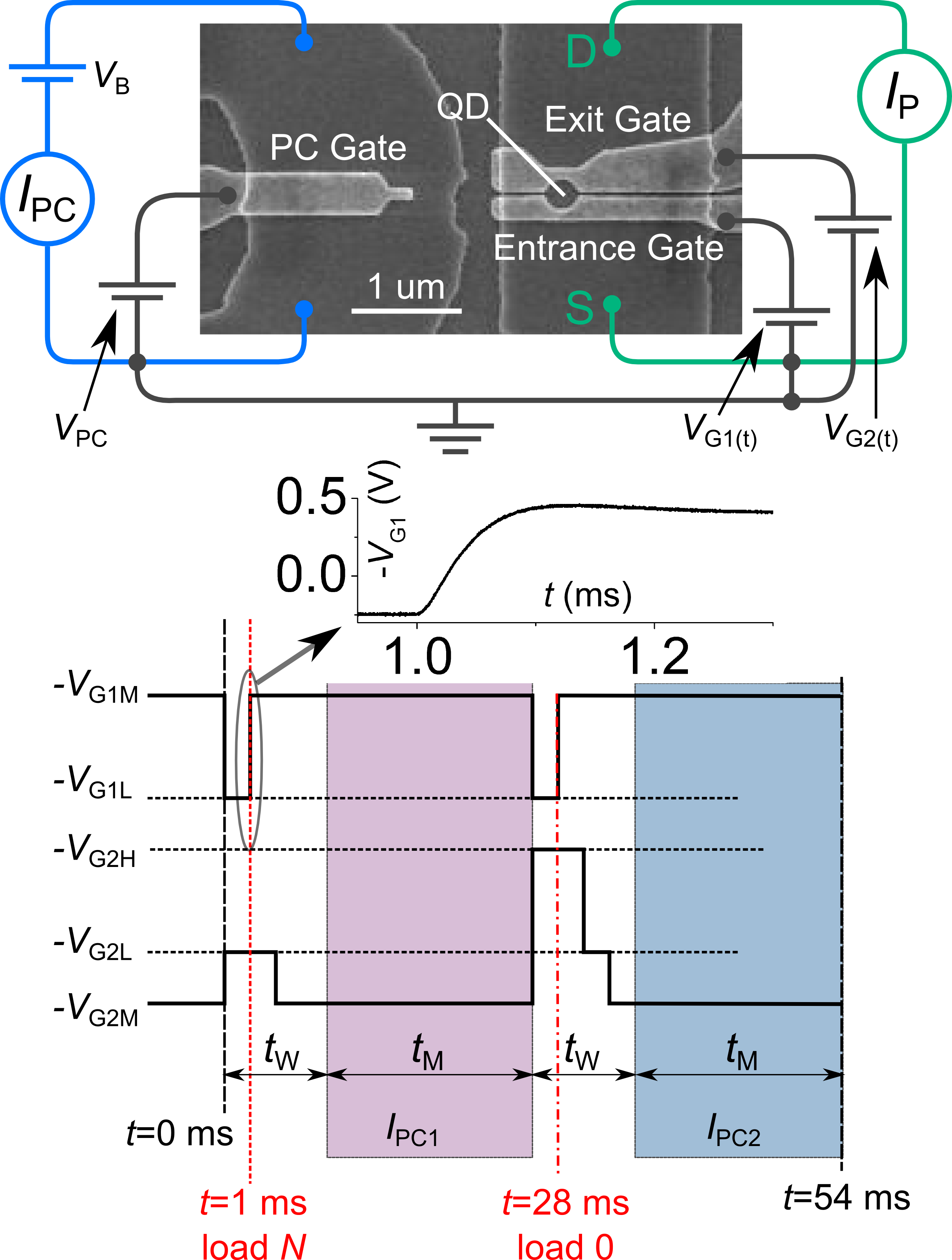
A scanning electron microscope image of a device similar to the one used in this study is shown in Fig. 1a. The device is fabricated on a wafer using wet etching to define two conducting channels (running from top to bottom in the figure) and electron-beam lithography to define metallic gates above the channels. The right-hand channel of the device is an electron pump similar to ones used in previous studies Giblin et al. (2012). Two metallic gates termed the entrance and exit gates supplied with voltages and deplete the 2-DEG and form a quantum dot (QD) in the circular cut-out region between the gates. The left-hand channel contains a point-contact charge detector. When the channel conductance is set close to pinch-off by applying a negative voltage to the point-contact gate, the conductance of the channel is a sensitive probe of the local charge environment Field et al. (1993). To maximise the sensitivity of the PC to the QD charge state, the QD is offset from the centre of the pump channel towards the PC.
In this work, the pump was operated in two modes. In the continuous pumping mode, the entrance gate was driven with an AC signal at frequency super-imposed on a DC voltage: , and the exit gate was supplied with a DC voltage . This has the effect of pumping electrons from source (S) to drain (D), and generating a current . In electron trapping mode, the PC channel was biased with a voltage mV, and was tuned to maximise . The pump gates were driven with the voltage sequence illustrated in Fig. 1b. At time , the entrance gate is pulsed to a positive voltage . This lowers the potential barrier under the gate and couples the QD to the source lead. At time ms (red vertical dashed line) the entrance gate is set to a negative voltage (the inset shows the rise time of this pulse). Depending on the setting of the exit gate , the negative-going switch of the entrance gate at ms may load electrons into the QD and possibly also eject some electrons to the drain, leaving the QD containing electrons. The charge state is probed by measuring the PC current for a time to yield a value . A wait time ensures that is not affected by the transient current induced by the entrance gate pulse. The pump gates couple strongly to the PC, and the adjustment of the entrance gate to at ms is a practical convenience which allows the readout of as a function of without continually re-tuning the PC gate voltage. To reduce the effect of noise in , the current reading was referenced to a second PC current measured with a known QD state . This state was obtained by setting the exit gate to a large negative value during the negative-going transition of the entrance gate (vertical dash-dot line at ms). The complete cycle of pump gate voltages yields a PC difference signal . For all the measurements reported here, V, V, ms and ms. The measurements were performed at a temperature of K.
III Results and Discussion
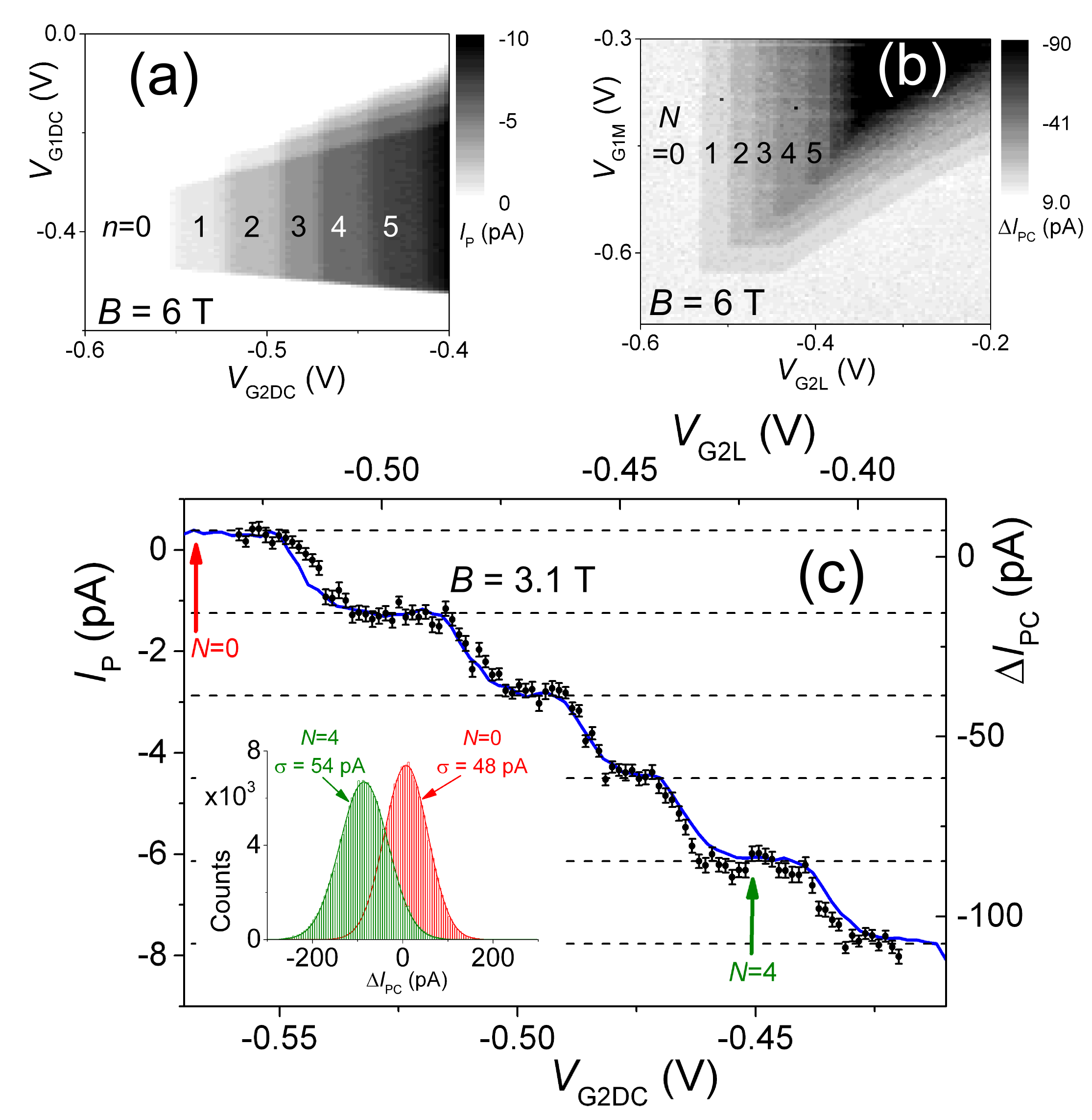
In Fig. 2(a) we show a grey-scale plot of as a function of and , with the device in continuous pumping mode in a perpendicular magnetic field of T. The series of quantised current plateaus corresponding to , where n is the number of electrons pumped for each cycle of , is a familiar characteristic of the tunable-barrier pump. Fig. 2(b) shows the corresponding map of with the device in trapping mode, and V. Each pixel in the plot results from averaging over 100 cycles of the type shown in Fig. 1b. The plot was constructed from scans of with constant and . Bands corresponding to a constant number of trapped electrons are clearly visible. As is increased from a large negative value, exhibits a step-wise increase, with the step position independent of . This is to be expected, since determines the energy above the Fermi level that the electrons are held, but does not affect the loading dynamics. If is increased sufficiently, decreases in a series of steps back down to zero. This is because the exit barrier is no longer high enough to maintain all the loaded electrons in the dot, and electrons are ejected to the drain McNeil et al. (2011). The truncation of the constant steps at large negative is an artefact caused by the choice of . For electrons can be ejected to the drain during the step of at ms. In the subsequent experiments reported here, we ensured that was sufficiently positive to avoid this artifact, and we verified that the results were independent of the choice of .
In Fig. 2c we compare the step-like increase of both and , with similar operating conditions at T. The entrance gate voltage in pump mode has been tuned so that all the electrons which are loaded from the source are also ejected to the drain. The x-axes of the plots have been shifted to bring them into alignment, but the scaling factor is the same. The overlap between the two types of data emphasises that the two modes of operation of the device are probing the same loading dynamics. Comparing the data of Fig. 2(b) and (c), it is apparent that the PC signal corresponding to one extra electron in the QD, is field-dependent. An offset pA in is visible in the data of Fig. 2(c). This is believed to be due to activation of trap states close to the PC (the offset in is a trivial pre-amp offset). The overall noise level in is illustrated by the histograms of , obtained at two values of corresponding to and (inset). It is clear from the width of the histograms that single-shot measurement of the charge state in one loading cycle is not possible in this sample. The different standard deviations obtained from Gaussian fits to the histograms are due to slightly different . We will return to discuss the noise and detection fidelity in a later section of this paper.
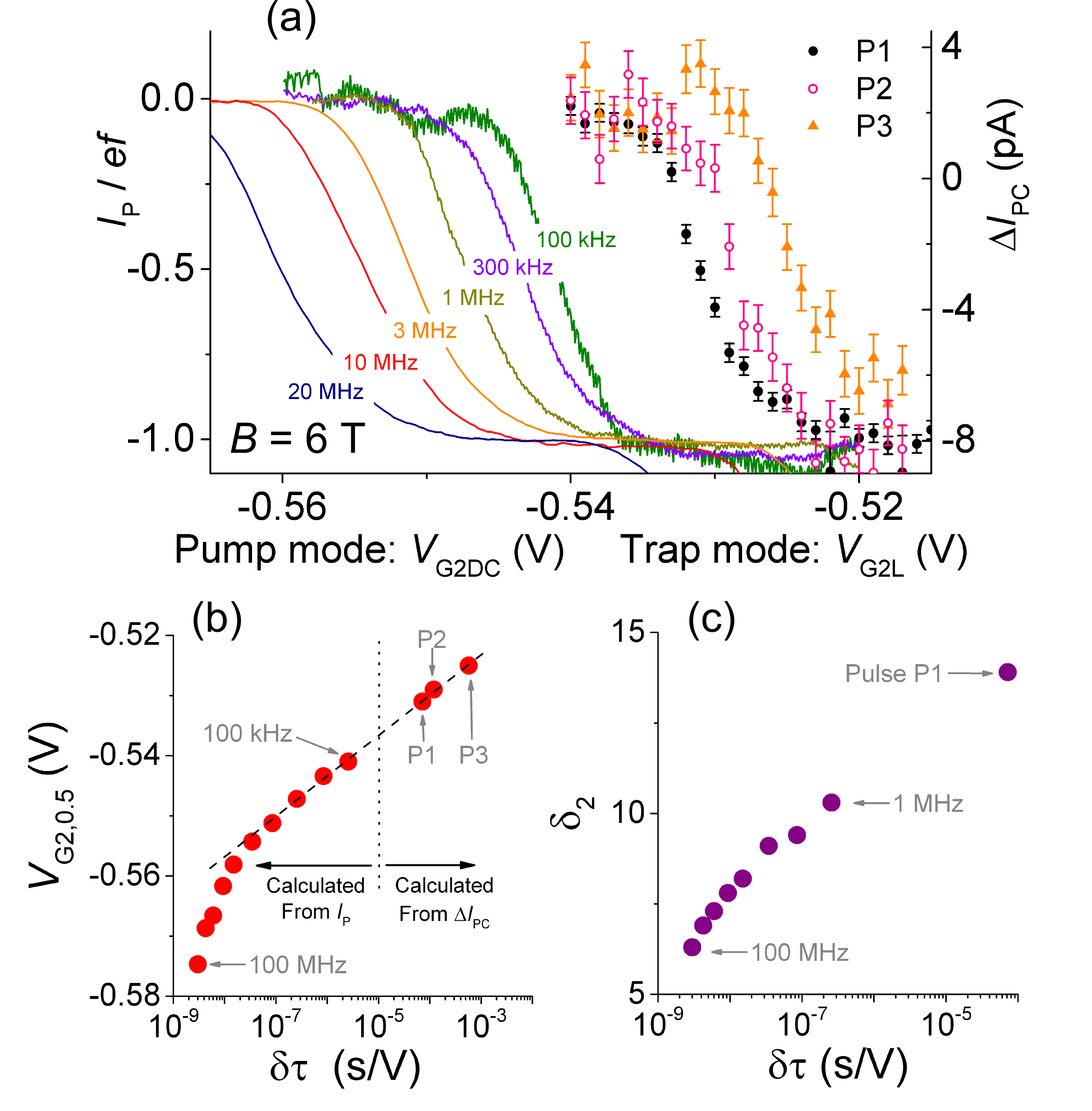
In the data of Fig. 3 we focus on the transition from loading zero electrons, to loading one electron into the QD. Fig 3a (solid lines,left axis) shows the pumped current with the pump driven at a range of relatively low frequencies. As the frequency is reduced, the plateau shifts to more positive exit gate voltage, and the width of the transition is slightly reduced. The current also becomes difficult to measure with the conventional ammeter used to measure in this experiment ( fA for kHz). Data points (right axis) show for three different entrance gate pulse rise-times, denoted . is as illustrated in the inset to Fig. 1(b), and and are progressively more heavily filtered with longer rise times. It has been predicted theoretically using the decay-cascade model Fujiwara et al. (2008); Kashcheyevs and Kaestner (2010), and verified experimentally over a limited range Fujiwara et al. (2008) that the plateaus positions shift to more positive exit gate voltage in proportion to where is the time-scale for raising the entrance barrier. is proportional to at the point in the cycle where the one-electron dot level rises above the Fermi level. We have defined . The choice of V is somewhat arbitrary, but the following results are almost completely independent of this choice in the plausible range of from V to V. We note that Fig. 2(b) shows that the QD is isolated from the source lead and containing a stable number of electrons for V. In Fig. 3(b) we show the shift of the plateau as a function of , where the shift is quantified as the exit gate voltage for which (pump data) or (trap data). Our measurement of using relatively slow loading pulses allows us to verify the expected shift in plateau position over four orders of magnitude in .
For MHz, we see deviation of the data of Fig. 3(b) from straight-line behaviour. This is due to significant distortion of the characteristic . The decay-cascade model only predicts a shift in the plateau along the axis, but not any change in the shape of the plateau as a function of the pumping time-scale. We fitted some of the data sets in Fig. 3(a) to the decay-cascade formula in the range and extracted the parameter , plotted in Fig. 3(c). A similar decrease in with increasing pumping frequency has been observed previously Giblin et al. (2012), but at much higher frequencies. The observation of this trend at relatively low frequencies, where capacitive cross-talk between the pump gates is expected to be negligible, is strong evidence that the decay-cascade model does not capture some key features of the pumping mechanism. The decoupling of a quantum dot from a reservoir by a rising tunnel barrier is a problem of general theoretical interest. More recent work includes extensions of the decay cascade model to include the effect of finite temperature in the leads Fricke et al. (2013); Yamahata et al. (2014), and a non-Markovian model including the energy scales associated with the time-dependence of the barrier height Kashcheyevs and Timoshenko (2012). Detailed comparisons of the predictions of these models with experimental data, as a function of barrier rise time, will be the subject of future research.
IV Simulation
We now consider whether single-shot detection of the QD charge state is possible in this type of experimental geometry. In Fig. 4(a) we show the noise spectrum of for the operating conditions of Fig.2c. This spectrum has a strong characteristic, which is commonly associated with the fluctuation of an ensemble of charged defects. For comparison we show the noise spectrum of the current pre-amplifier connected to a dummy load designed to simulate the electrical impedance of the PC and its associated wiring ( nF in parallel with k). It is likely that the PC in our experiment exhibits excess noise because it is formed at the edge of a chemical-etched channel which contains a high density of charged defects. Alternative device designs can form the PC using electrostatic gates only, and in the following discussion we will assume that the experimental noise will be dominated by the loaded pre-amp noise. We used a numerical simulation to generate noise with a similar frequency spectrum to the loaded pre-amp (black line in Fig. 4a) and then used this noise as an input to a simulation of the experimental protocol illustrated in Fig. 1b. For a given and the output of the simulation is a histogram of (points in Fig. 4b), which we fit to a Gaussian function (solid line in Fig. 4b). The ability of the experiment to distinguish charge states differing by one electron depends on the width of this histogram, and the sensitivity of to a change in of one, denoted . In Fig. 4b we illustrated the state, for the case where pA, i.e. twice the experimentally measured value. We define a threshold current , and assign the state or to measurements with and respectively. The probability of assigning the wrong charge state to a measurement result is simply the integral of from to infinity, where is the normalised probability distribution of obtaining a value in a single measurement cycle. To ensure , as is generally needed for primary electrical metrology, we require . Thus, for pA obtained in the simulation, we require pA, or more than four times the measured value of pA. Planar QD-PC systems with optimised geometry have demonstrated pA with mV Vandersypen et al. (2004), and sensitivities an order of magnitude larger have been demonstrated with vertical QD-PC geometry Gustavsson et al. (2008).
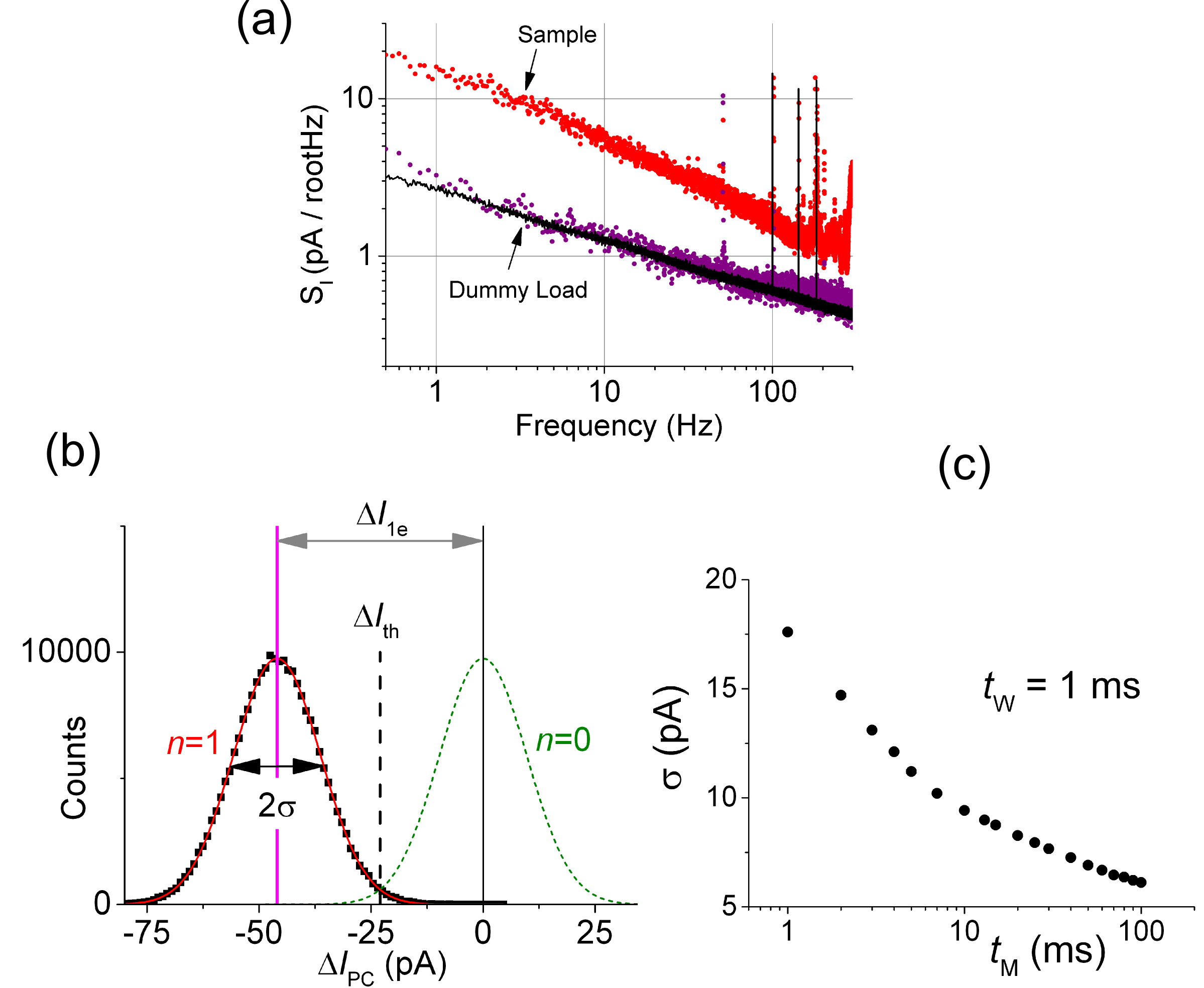
Finally, we consider the possibility of completing the required large number of test cycles in a reasonable time-scale. For ms, ms, cycles would take days. By shortening the measurement and wait times, more test cycles can be completed at the expense of a lower detection fidelity. Fig 4c shows for simulated data, with ms and variable . For ms, one cycle takes ms and cycles could be completed in hours, although is now pA, requiring pA in order to maintain the detection fidelity at the level. The overall cycle time could be shortened further, because for ms, is determined mainly by frequency-independent noise and it is not necessary to perform an reference cycle for every loading cycle. Using ms in the simulations assumes the use of a current pre-amplifier with a shorter settling time than the one used in the experiments reported here, but this is well within the achievable specifications for room-temperature Kretinin and Chung (2012) and cryogenic Vink et al. (2007) current pre-amplifiers.
V conclusions
Using the methodology presented in this paper, metrological error-detection on the tunable barrier pump is feasible with modest improvements to the PC-QD coupling sensitivity, and the bandwidth of the current pre-amplifier used to measure the PC current. Using an arbitrary waveform generator to drive the pump entrance gate, the loading and ejection errors can be investigated separately. More generally, the initialisation of a dynamic quantum dot can be investigated over a very wide range of the decoupling rate of the dot from the leads, including slow rates not accessible by measuring the pumped current. This should improve our ability to distinguish between different models for the dot initialisation process.
Acknowledgements.
This research was supported by the UK department for Business, Innovation and Skills and within the Joint Research Project ”‘Quantum Ampere”’ (JRP SIB07) within the European Metrology Research Programme (EMRP). The EMRP is jointly funded by the EMRP participating countries within EURAMET and the European Union.References
- Blumenthal et al. (2007) M. D. Blumenthal, B. Kaestner, L. Li, S. P. Giblin, T. J. B. M. Janssen, M. Pepper, D. Anderson, G. A. C. Jones, and D. A. Ritchie, Nature Physics 3, 343 (2007).
- Kaestner et al. (2008) B. Kaestner, V. Kashcheyevs, S. Amakawa, M. D. Blumenthal, L. Li, T. J. B. M. Janssen, G. Hein, K. Pierz, T. Weimann, U. Siegner, et al., Physical Review B 77, 153301 (2008).
- Fujiwara et al. (2008) A. Fujiwara, K. Nishiguchi, and Y. Ono, Applied Physics Letters 92, 042102 (2008).
- Jehl et al. (2013) X. Jehl, B. Voisin, T. Charron, P. Clapera, S. Ray, B. Roche, M. Sanquer, S. Djordjevic, L. Devoille, R. Wacquez, et al., Physical Review X 3, 021012 (2013).
- Rossi et al. (2014) A. Rossi, T. Tanttu, K. Y. Tan, I. Iisakka, R. Zhao, K. W. Chan, G. C. Tettamanzi, S. Rogge, A. S. Dzurak, and M. Mottonen, Nano letters (2014).
- Giblin et al. (2012) S. Giblin, M. Kataoka, J. Fletcher, P. See, T. Janssen, J. Griffiths, G. Jones, I. Farrer, and D. Ritchie, Nature Communications 3, 930 (2012).
- Feltin et al. (2003) N. Feltin, L. Devoille, F. Piquemal, S. V. Lotkhov, and A. B. Zorin, Instrumentation and Measurement, IEEE Transactions on 52, 599 (2003).
- Keller (2008) M. W. Keller, Metrologia 45, 102 (2008).
- Martinis et al. (1994) J. M. Martinis, M. Nahum, and H. D. Jensen, Physical review letters 72, 904 (1994).
- Keller et al. (1996) M. W. Keller, J. M. Martinis, N. M. Zimmerman, and A. H. Steinbach, Applied physics letters 69, 1804 (1996).
- Camarota et al. (2012) B. Camarota, H. Scherer, M. W. Keller, S. V. Lotkhov, G.-D. Willenberg, and F. J. Ahlers, Metrologia 49, 8 (2012).
- Fricke et al. (2013) L. Fricke, M. Wulf, B. Kaestner, V. Kashcheyevs, J. Timoshenko, P. Nazarov, F. Hohls, P. Mirovsky, B. Mackrodt, R. Dolata, et al., Physical Review Letters 110, 126803 (2013).
- Yamahata et al. (2014) G. Yamahata, K. Nishiguchi, and A. Fujiwara, Physical Review B 89, 165302 (2014).
- Fricke et al. (2014) L. Fricke, M. Wulf, B. Kaestner, F. Hohls, P. Mirovsky, B. Mackrodt, R. Dolata, T. Weimann, K. Pierz, U. Siegner, et al., Phys. Rev. Lett. 112, 226803 (2014), URL http://link.aps.org/doi/10.1103/PhysRevLett.112.226803.
- Vandersypen et al. (2004) L. Vandersypen, J. Elzerman, R. Schouten, L. W. Van Beveren, R. Hanson, and L. Kouwenhoven, Applied Physics Letters 85, 4394 (2004).
- Elzerman et al. (2004) J. Elzerman, R. Hanson, L. Van Beveren, B. Witkamp, L. Vandersypen, and L. Kouwenhoven, Nature 430, 431 (2004).
- Cooper et al. (2000) J. Cooper, C. Smith, D. Ritchie, E. Linfield, Y. Jin, and H. Launois, Physica E: Low-dimensional Systems and Nanostructures 6, 457 (2000).
- Field et al. (1993) M. Field, C. Smith, M. Pepper, D. Ritchie, J. Frost, G. Jones, and D. Hasko, Physical review letters 70, 1311 (1993).
- McNeil et al. (2011) R. McNeil, M. Kataoka, C. Ford, C. Barnes, D. Anderson, G. Jones, I. Farrer, and D. Ritchie, Nature 477, 439 (2011).
- Kashcheyevs and Kaestner (2010) V. Kashcheyevs and B. Kaestner, Physical Review Letters 104, 186805 (2010).
- Kashcheyevs and Timoshenko (2012) V. Kashcheyevs and J. Timoshenko, Physical review letters 109, 216801 (2012).
- Gustavsson et al. (2008) S. Gustavsson, I. Shorubalko, R. Leturcq, S. Schön, and K. Ensslin, Applied Physics Letters 92, 152101 (2008).
- Kretinin and Chung (2012) A. V. Kretinin and Y. Chung, Review of Scientific Instruments 83, 084704 (2012).
- Vink et al. (2007) I. Vink, T. Nooitgedagt, R. Schouten, L. Vandersypen, and W. Wegscheider, Applied Physics Letters 91, 123512 (2007).