Bulk-impurity induced noise in large-area epitaxial thin films of topological insulators
Abstract
We report a detailed study of low-frequency -noise in large-area molecular-beam epitaxy grown thin ( nm) films of topological insulators as a function of temperature, gate voltage and magnetic field. When the fermi energy is within the bulk valence band, the temperature dependence reveals a clear signature of generation-recombination noise at the defect states in the bulk band gap. However, when the fermi energy is tuned to the bulk band gap, the gate voltage dependence of noise shows that the resistance fluctuations in surface transport are caused by correlated mobility-number density fluctuations due to the activated defect states present in the bulk of the topological insulator crystal with a density cm-2eV-1. In the presence of magnetic field, noise in these materials follows a parabolic dependence which is qualitatively similar to mobility and charge-density fluctuation noise in non-degenerately doped trivial semiconductors. Our studies reveal that even in thin films of (Bi,Sb)2Te3 with thickness as low as 10 nm, the internal bulk defects are the dominant source of noise.
Topological insulators (TIs) are characterized by gapless linearly dispersive spin-polarized surface states in the bulk band gap Rev3Qi2011 ; ZahidHasanRevModPhys.82.3045 . These materials are promising candidates for various electronic and spintronic applications Rev4Kong2011 due to the topological protection of surface states against back scattering from non-magnetic impurities. However, sensitivity of these surface states to different types of disorder is still a matter of active debate TiMobility3 ; TiMobility4 ; ImpScat1 ; impurityScatter ; Mypaper ; Adam2012 ; Black-Schaffer2012 . Recently, flicker noise or -noise in bulk TI systems has been established as a powerful tool not only as a performance-marker for electronic applications but also for defect-spectroscopy and even band structure determination Mypaper ; My_apl ; Noise_TI_cascales2015band . Noise measurements in exfoliated TI devices from bulk crystals have revealed that in the thickness range of nm to 80 m charge number fluctuations in the bulk can give rise to the resistance fluctuations in the surface states Mypaper . For nm thick exfoliated films however, the underlying disorder dynamics could not be determined as noise was dominated by universal conductance fluctuations (UCF), since lateral dimension of this device (800 nm nm) turned out to be of the same order as the phase coherence length ( nm) itself. However, devices in this thickness range are arguably most suitable for novel applications Spintronic1 ; Sacepe2011 ; SpinPolarizationDetect ; NitinTiSpinTorque ; Magswitching ; proximity_lang2014proximity , as this thickness is low enough to allow the bottom gate to tune the chemical potential at both top and bottom surfaces top_bot_PhysRevB.83.241304 ; SixQPLimit ; Kim2012a , albeit high enough to prevent any overlap between two surface states which can result in a gap at the Dirac point hybrid_lu2010massive . Hence, it is important to evaluate and understand noise in 3D TI devices with thickness nm. In this work, we have studied large area (1 mm0.5 mm) TI films with nm thickness, where mesoscopic conductance fluctuations are averaged out and underlying defect fluctuations can be detected.
The devices studied in this paper were fabricated from thin (thickness, nm) films of (Bi,Sb)2Te3 (BST) grown by molecular beam epitaxy on SrTiO3 (STO) substrates with a metallic back-coating of Indium that is used as back gate electrode eeFMTI1_kandala2013growth . All the measurements, except temperature () dependence of -noise, were performed in device BST1 (gate voltage at charge neutrality point V and 71 V at two consecutive thermal cycles). The -dependence of noise was performed in BST2 ( V). Both devices were intrinsically hole-doped. Hall bar geometry with a channel length of 1 mm and width 0.5 mm was defined by mechanical patterning (inset, Fig. 1a). While, non-invasive hall bar geometry minimizes contribution of contacts in electrical transport and noise measurements karnatak2016current ; Ghatak2014 , the mechanical etching process prevents the film from being exposed to chemicals (e-beam resist and solvents), resulting in a superior surface quality. The large dielectric constant of the STO substrate at cryogenic temperatures allows effective electrical back gating for tuning the chemical potential in the sample STO_TI4tian2014quantum ; STO_TI3:/content/aip/journal/apl/101/12/10.1063/1.4754108 ; Kim2012a . Electrical transport and noise measurements were conducted down to K and up to magnetic field of 13 T.
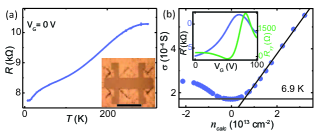
The decrease in resistance () with decreasing (Fig. 1a) indicates metallic behavior, which is similar to the - behavior reported previously in similar thin exfoliated TI devices with negligible bulk conduction Mypaper . However, in this case, the measured intrinsic Hall number density is cm-2 (at K and gate voltage V), which is high compared to typical number density of surface charge carriers in TI STO_TI4tian2014quantum , indicating that the Fermi energy is located within the valence band, and holes in the bulk of the material are mainly responsible for such metallic behavior. This intrinsic high doping leads to a high value of the gate voltage ( V), at charge neutrality point, which is identified by a maximum in the and a change of sign in transverse resistance (inset, Fig. 1b). In order to evaluate the extent of disorder, we have fitted - data (Fig 1b) (where and within the framework of charge-impurity limited scattering of Dirac fermions sigma_nculcer2010two ; Kim2012a , so that
| (1) |
and
| (2) |
where is the residual carrier density in electron and hole puddles, and is a constant that depends on the Wigner–Seitz radius . The extracted value of number density of Coulomb trap is cm-2, which is quite high compared to typical density of Coulomb traps at oxide-channel interface in graphene-FETs chen2008charged , but matches well with the number density of charged disorders in TI-devices Kim2012a , and can be attributed to the bulk charged-defects in TI.
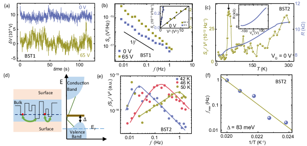
An AC four-probe Wheatstone bridge technique was used for noise measurements scofield1987ac ; SaquibPRB . The voltage fluctuations as shown in Fig. 2a were recorded as a function of time using a 16-bit digitizer. The time-series data were then digitally processed to obtain the power-spectral-density (PSD, ) as a function of frequency () (Fig 2b). In both devices, we found , where the frequency exponent . The shows a quadratic dependence with bias () (inset, Fig. 2b), which ensures that we are in the Ohmic regime.
In device BST2, the chemical potential is intrinsically located within the valence band and only the bulk electronic states contribute to transport ( changes by less than over the entire gate voltage range of (inset, Fig. 2c)). The magnitude of noise ( at Hz) (Fig. 2c) shows a gradual increase with increasing along with a strong peak at K. The gradual increase in noise can be associated with thermally activated defect dynamics in metallic diffusive systems activated_raychaudhuri2002flicker . The strong peak in noise magnitude at K bears close resemblance to the noise maximum associated with bulk generation-recombination (G-R) process, which was reported recently for mechanically exfoliated heavily-doped TI devices Mypaper . The process is schematically explained in Fig. 2d, which is a characteristic feature of Bi-chalcogenide-based TI devices that depends on the energetics of the impurity bands. In order to confirm the G-R mechanism for the noise peak at K, we note the timescale associated with this process () gives rise to a frequency maximum () in the power spectral density (PSD) at temperatures close to the peak (Fig. 2e). The value of the energy gap associated, as obtained from the fitting of activated behavior of (Fig. 2f) as a function of is meV, which indicates that the impurity band responsible for this noise is located at meV above the bulk valence band
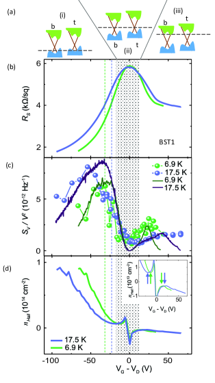
The -dependence of sheet-resistance () shows graphene-like atinapl ; AtinACSNano ; atin_apl_cvd ambipolar transport at both 6.9 K and 17.5 K (Fig. 3b). The increase of at the higher is caused by the reduction of dielectric constant of STO hong2011ultra . Voltage normalized power spectral density , i.e., the magnitude of noise is shown as a function of effective gate voltage at 6.9 K and 17.5 K (Fig. 3c). It is minimum close to the Dirac point , but increases rapidly ( times) with increasing , and reaches a maximum (at V, at 6.9 K). With further increase in , noise magnitude reduces.
To correlate this behavior with the nature and sign of the charge carrying species, we have measured the Hall number density () as a function of at 6.9 K. Change in the back-gate capacitance was estimated from the - data, and used to extract the dependence of at 17.5 K. Fig. 3d shows that the back-gate can tune the state of doping from p-type to n-type over the entire device. Our data clearly illustrates that the noise magnitude is enhanced for cm-2 on the hole side, which is the number density associated with the edge of the bulk valence band STO_TI4tian2014quantum ; Kim2012a , demonstrating increased impact of disorder on the bulk charge transport as expected. Due to non-linear dependence of capacitance on STO_TI4tian2014quantum , the number density in the accessible range of did not increase beyond cm-2 in the electron-side, and hence the noise magnitude saturated to a lower value.
In Fig. 3d the two extrema at the number density (e.g. V and 15.7 V, at 6.9 K) indicate the transition from pseudo-diffusive (shaded area) to diffusive electrical transport STO_TI3:/content/aip/journal/apl/101/12/10.1063/1.4754108 ; STO_TI4tian2014quantum . However, unlike mesoscopic devices of graphene AtinACSNano ; Rossipaper1 or TIs Mypaper , the noise does not show any specific signature at these transition points in our device as mesoscopic effects average out in the large area thin films where ( and are length and width of the channel).
For a more quantitative understanding, we have fitted the -dependence of data (Fig 3c) using the framework of correlated mobility-number density fluctuations model Jayaraman1989 . According to this model, the noise in the channel is affected by the trapping-detrapping of charges in gate dielectric-channel interface (Fig. 2d). The main components of the noise are,
1. The fluctuations of the number of charge carriers in the channel due to tunneling to and from the oxide traps at the channel-gate dielectric interface.
2. The mobility fluctuations caused by the Coulomb scattering induced by fluctuating trapped charges.
The total noise can be expressed as,
| (3) |
where represents a pure number fluctuation, represents pure mobility fluctuations and represents combined number and mobility fluctuations ( is the decay constant for the spatially decaying time constant of a typical trapping event and is the scattering constant) and can be evaluated using phenomenological values Jayaraman1989 . , , , , , , are the areal trapped charge density per unit energy, Boltzmann constant, width of the channel, length of the channel, conductance and number density of charge carriers, axis in the direction perpendicular to the channel respectively, Hz frequency and nm is the distance over which the tunneling is effective. The data at 6.9 K and 17.5 K were fitted independently to extract the values of . We found, cm-2eV-1 at 6.9 K, which is several orders of magnitude higher compared to typical trap density at oxide surface Jayaraman1989 ; paul2016percolative . However, considering an energy window of , the number of activated trapped states, cm-2, which matches with the number density of Coulomb traps cm-2, extracted from the fitting of the - (Fig. 1b) showing that the extracted value of is not an artefact and hence this high density of charge impurities can be attributed to intrinsic bulk defect states in (Bi,Sb)2Te3 Kim2012a . Similar ( cm-2eV-1) was found for 17.5 K. The origin of the slight elevation of noise magnitude at 17.5 K can be attributed to the thermal activation of the charge-defects.
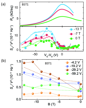
We have performed magnetic field () dependent measurement of noise in our devices to verify the correlated charge and mobility fluctuation-related origin of noise. In the entire range of ( V to 21 V) the noise follows a parabolic dependence with magnetic field (Fig. 4b) which also reflects in the -dependence of noise at different values of magnetic field (Fig. 4a). Drude theory of metals predicts this type of behavior for a charge-fluctuation or mobility fluctuation type noise in a non-degenerately doped semiconductor with ( where cm2/V.s is the Hall mobility) Noise_B1_kleinpenning19801 ; Noise_B2_voorde1981magnetic . Fig. 4a and b shows fit of this data according to the eq.
| (4) |
Here, is a fitting parameter. Although in our devices, the extracted value of is quite high compared to the theoretical value expected for charge or mobility fluctuation noise Noise_B2_voorde1981magnetic . In the absence of a theory which accounts for the magnetic field dependence of correlated mobility-number density fluctuation noise for a doped semiconductor, we cannot comment whether this strong dependence on magnetic field results from simple geometric effects or is a consequence of the topological nature of the charge-carriers. However, we note that the behavior does not change as the chemical potential is tuned through surface and bulk bands of topological insulators.
The results of our experiments clearly indicate that even in thin films of topological insulator (BiSb)2Te3 with thickness as low as nm, the bulk chalcogenide defects are mainly responsible for resistance fluctuations for both surface and bulk electronic states. Whereas for the bulk valence band, generation-recombination processes in between the valence band and the impurity states are the main reason of resistance fluctuations, the noise at the surface states are caused by the correlated mobility-charge density fluctuation caused by trapping-detrapping of surface charge carriers by the charged-defects in the bulk of the crystal. This scenario is different from our earlier study of noise in thicker exfoliated topological insulator devices Mypaper where generation recombination of charge carriers at the bulk gives rise to a fluctuation of potential landscape at the surface which results in a mobility fluctuation noise. Further theoretical understanding is needed for the strong magnetic field dependence of noise in topological insulators.
AG, SB and SI acknowledge support from DST, India. AR and NS acknowledge support from The Pennsylvania State University Two-Dimensional Crystal Consortium – Materials Innovation Platform (2DCC-MIP) which is supported by NSF cooperative agreement DMR-1539916.
References
- (1) X.-L. Qi and S.-C. Zhang, “Topological insulators and superconductors,” Rev. Mod. Phys., vol. 83, p. 1057, 2011.
- (2) M. Z. Hasan and C. L. Kane, “Colloquium: Topological insulators,” Rev. Mod. Phys., vol. 82, pp. 3045–3067, Nov 2010.
- (3) D. Kong and Y. Cui, “Opportunities in chemistry and materials science for topological insulators and their nanostructures,” Nat. Chem., vol. 3, no. October, pp. 845–849, 2011.
- (4) G. Yin, D. Wickramaratne, Y. Zhao, and R. K. Lake, “Coulomb impurity scattering in topological insulator thin films,” Appl. Phys. Lett., vol. 105, p. 033118, 2014.
- (5) D. X. Qu, S. K. Roberts, and G. F. Chapline, “Observation of huge surface hole mobility in the topological insulator Bi0.91Sb0.09 (111),” Phys. Rev. Lett., vol. 111, no. OCTOBER, p. 176801, 2013.
- (6) Z. Alpichshev, R. R. Biswas, A. V. Balatsky, J. G. Analytis, J. H. Chu, I. R. Fisher, and A. Kapitulnik, “STM imaging of impurity resonances on Bi2Se3,” Phys. Rev. Lett., vol. 108, no. May, p. 206402, 2012.
- (7) L. Wu, M. Brahlek, R. Valdés Aguilar, a. V. Stier, C. M. Morris, Y. Lubashevsky, L. S. Bilbro, N. Bansal, S. Oh, and N. P. Armitage, “A sudden collapse in the transport lifetime across the topological phase transition in (Bi1-xInx)2Se3,” Nat. Phys., vol. 9, pp. 410–414, Jul 2013.
- (8) S. Bhattacharyya, M. Banerjee, H. Nhalil, S. Islam, C. Dasgupta, S. Elizabeth, and A. Ghosh, “Bulk-Induced 1/f Noise at the Surface of Three-Dimensional Topological Insulators,” ACS Nano, vol. 9, no. 12, pp. 12529–12536, 2015.
- (9) S. Adam, E. H. Hwang, and S. Das Sarma, “Two-dimensional transport and screening in topological insulator surface states,” Phys. Rev. B, vol. 85, p. 235413, 2012.
- (10) A. M. Black-Schaffer and A. V. Balatsky, “Subsurface impurities and vacancies in a three-dimensional topological insulator,” Phys. Rev. B, vol. 86, p. 115433, Sep 2012.
- (11) S. Bhattacharyya, A. Kandala, A. Richardella, S. Islam, N. Samarth, and A. Ghosh, “Resistance noise in epitaxial thin films of ferromagnetic topological insulators,” Appl. Phys. Lett., vol. 108, no. 8, p. 082101, 2016.
- (12) J. P. Cascales, I. Martínez, F. Katmis, C.-Z. Chang, R. Guerrero, J. S. Moodera, and F. G. Aliev, “Band structure of topological insulators from noise measurements in tunnel junctions,” Appl. Phys. Lett., vol. 107, no. 25, p. 252402, 2015.
- (13) A. A. Baker, A. I. Figueroa, L. J. Collins-McIntyre, G. van der Laan, and T. Hesjedal, “Spin pumping in Ferromagnet-Topological Insulator-Ferromagnet Heterostructures,” Sci. Rep., vol. 5, p. 7907, 2015.
- (14) B. Sacépé, J. B. Oostinga, J. Li, A. Ubaldini, N. J. G. Couto, E. Giannini, and A. F. Morpurgo, “Gate-tuned normal and superconducting transport at the surface of a topological insulator.,” Nat. Commun., vol. 2, p. 575, Jan. 2011.
- (15) Y. Ando, T. Hamasaki, T. Kurokawa, K. Ichiba, F. Yang, M. Novak, S. Sasaki, K. Segawa, Y. Ando, and M. Shiraishi, “Electrical Detection of the Spin Polarization Due to Charge Flow in the Surface State of the Topological Insulator Bi1.5Sb0.5Te1.7Se1.3,” Nano Lett., vol. 14, no. 11, pp. 6226–6230, 2014.
- (16) A. R. Mellnik, J. S. Lee, A. Richardella, J. L. Grab, P. J. Mintun, M. H. Fischer, A. Vaezi, A. Manchon, E.-A. Kim, N. Samarth, and D. C. Ralph, “Spin-transfer torque generated by a topological insulator,” Nature, vol. 511, pp. 449–451, 2014.
- (17) Y. Fan, P. Upadhyaya, X. Kou, M. Lang, S. Takei, Z. Wang, J. Tang, L. He, L.-T. Chang, M. Montazeri, G. Yu, W. Jiang, T. Nie, R. N. Schwartz, Y. Tserkovnyak, and K. L. Wang, “Magnetization switching through giant spin-orbit torque in a magnetically doped topological insulator heterostructure,” Nat. Mater., vol. 13, pp. 699–704, Jul 2014.
- (18) M. Lang, M. Montazeri, M. C. Onbasli, X. Kou, Y. Fan, P. Upadhyaya, K. Yao, F. Liu, Y. Jiang, W. Jiang, et al., “Proximity induced high-temperature magnetic order in topological insulator-ferrimagnetic insulator heterostructure,” Nano Lett., vol. 14, pp. 3459–3465, May 2014.
- (19) J. Chen, X. Y. He, K. H. Wu, Z. Q. Ji, L. Lu, J. R. Shi, J. H. Smet, and Y. Q. Li, “Tunable surface conductivity in Bi2Se3 revealed in diffusive electron transport,” Phys. Rev. B, vol. 83, p. 241304, Jun 2011.
- (20) Y. Zhang, K. He, C.-Z. Chang, C.-L. Song, L.-l. Wang, X. Chen, J.-F. Jia, Z. Fang, X. Dai, W.-Y. Shan, S.-Q. Shen, Q. Niu, X.-L. Qi, and S.-C. Zhang, “Crossover of the three-dimensional topological insulator Bi2Se3 to the two-dimensional limit,” Nat. Phys., vol. 6, pp. 584–588, Aug 2010.
- (21) D. Kim, S. Cho, N. P. Butch, P. Syers, K. Kirshenbaum, S. Adam, J. Paglione, and M. S. Fuhrer, “Surface conduction of topological Dirac electrons in bulk insulating Bi2Se3,” Nat. Phys., vol. 8, pp. 459–463, April 2012.
- (22) H.-Z. Lu, W.-Y. Shan, W. Yao, Q. Niu, and S.-Q. Shen, “Massive Dirac fermions and spin physics in an ultrathin film of topological insulator,” Phys. Rev. B, vol. 81, p. 115407, Mar 2010.
- (23) A. Kandala, A. Richardella, D. Rench, D. Zhang, T. Flanagan, and N. Samarth, “Growth and characterization of hybrid insulating ferromagnet-topological insulator heterostructure devices,” Appl. Phys. Lett., vol. 103, no. 20, p. 202409, 2013.
- (24) P. Karnatak, T. P. Sai, S. Goswami, S. Ghatak, S. Kaushal, and A. Ghosh, “Current crowding mediated large contact noise in graphene field-effect transistors,” Nat. Commun., vol. 7, p. 13703, 2016.
- (25) S. Ghatak, S. Mukherjee, M. Jain, and D. D. Sarma, “Microscopic origin of low frequency noise in MoS2 field-effect transistors,” APL Mater., vol. 2, p. 092515, Sep 2014.
- (26) J. Tian, C. Chang, H. Cao, K. He, X. Ma, Q. Xue, and Y. P. Chen, “Quantum and classical magnetoresistance in ambipolar topological insulator transistors with gate-tunable bulk and surface conduction,” Sci. Rep., vol. 4, p. 4859, 2014.
- (27) X. He, T. Guan, X. Wang, B. Feng, P. Cheng, L. Chen, Y. Li, and K. Wu, “Highly tunable electron transport in epitaxial topological insulator (Bi1-xSbx)2Te3 thin films,” Appl. Phys. Lett., vol. 101, no. 12, p. 123111, 2012.
- (28) D. Culcer, E. Hwang, T. D. Stanescu, and S. D. Sarma, “Two-dimensional surface charge transport in topological insulators,” Phys. Rev. B, vol. 82, no. 15, p. 155457, 2010.
- (29) J.-H. Chen, C. Jang, S. Adam, M. Fuhrer, E. Williams, and M. Ishigami, “Charged-impurity scattering in graphene,” Nat. Phys., vol. 4, no. 5, pp. 377–381, 2008.
- (30) J. H. Scofield, “ac method for measuring low-frequency resistance fluctuation spectra,” Rev. Sci. Instrum., vol. 58, no. 6, pp. 985–993, 1987.
- (31) S. Shamim, S. Mahapatra, C. Polley, M. Y. Simmons, and A. Ghosh, “Suppression of low-frequency noise in two-dimensional electron gas at degenerately doped Si:P layers,” Phys. Rev. B, vol. 83, p. 233304, Jun 2011.
- (32) A. Raychaudhuri, A. Ghosh, and S. Kar, “Flicker noise in degenerately doped si single crystals near the metal-insulator transition,” Pramana-J. Phys., vol. 58, p. 343, 2002.
- (33) A. N. Pal and A. Ghosh, “Ultralow noise field-effect transistor from multilayer graphene,” Appl. Phys. Lett., vol. 95, p. 082105, Aug 2009.
- (34) A. N. Pal, S. Ghatak, V. Kochat, and A. Sampathkumar, “Microscopic Mechanism of 1/f Noise in Graphene: Role of Energy Band Dispersion,” ACS Nano., vol. 5, pp. 2075–2081, Feb 2011.
- (35) A. N. Pal, A. A. Bol, and A. Ghosh, “Large low-frequency resistance noise in chemical vapor deposited graphene,” Appl. Phys. Lett., vol. 97, p. 133504, Sep 2010.
- (36) S. S. Hong, J. J. Cha, D. Kong, and Y. Cui, “Ultra-low carrier concentration and surface dominant transport in sb-doped bi2se3 topological insulator nanoribbons,” Nat. Commun., vol. 3, p. 757, 2011.
- (37) E. Rossi, J. H. Bardarson, M. S. Fuhrer, and S. Das Sarma, “Universal Conductance Fluctuations in Dirac Materials in the Presence of Long-range Disorder,” Phys. Rev. Lett., vol. 109, p. 096801, Aug. 2012.
- (38) R. Jayaraman and C. G. Sodini, “ Noise Technique To Extract the Oxide Trap Density Near the Conduction Band Edge of Silicon,” IEEE T. Electron Dev., vol. 36, no. 9, pp. 1773–1782, 1989.
- (39) T. Paul, S. Ghatak, and A. Ghosh, “Percolative switching in transition metal dichalcogenide field-effect transistors at room temperature,” Nanotechnol., vol. 27, no. 12, p. 125706, 2016.
- (40) T. G. Kleinpenning, “1/f noise in hall effect: Fluctuations in mobility,” J. Appl. Phys., vol. 51, no. 6, pp. 3438–3438, 1980.
- (41) P. V. Voorde and W. Love, “Magnetic effects on 1 f noise in n-insb,” Phys. Rev. B, vol. 24, no. 8, p. 4781, 1981.
- (42) M. J. Deen, J. Ilowski, and P. Yang, “Low frequency noise in polysilicon-emitter bipolar junction transistors,” J. Appl. Phys., vol. 77, no. 12, pp. 6278–6288, 1995.
.