Interlayer hybridization and moiré superlattice minibands for electrons and excitons in heterobilayers of transition-metal dichalcogenides
Abstract
Geometrical moiré patterns, generic for almost aligned bilayers of two-dimensional (2D) crystals with similar lattice structure but slightly different lattice constants, lead to zone folding and miniband formation for electronic states. Here, we show that moiré superlattice (mSL) effects in MoSe2/WS2 and MoTe2/MoSe2 heterobilayers that feature alignment of the band edges are enhanced by resonant interlayer hybridization, and anticipate similar features in twisted homobilayers of TMDs, including examples of narrow minibands close to the actual band edges. Such hybridization determines the optical activity of interlayer excitons in transition-metal dichalcogenide (TMD) heterostructures, as well as energy shifts in the exciton spectrum. We show that the resonantly hybridized exciton (hX) energy should display a sharp modulation as a function of the interlayer twist angle, accompanied by additional spectral features caused by umklapp electron-photon interactions with the mSL. We analyze the appearance of resonantly enhanced mSL features in absorption and emission of light by the interlayer exciton hybridization with both intralayer A and B excitons in MoSe2/WS2, MoTe2/MoSe2, MoSe2/MoS2, WS2/MoS2, and WSe2/MoSe2.
I Introduction
Van der Waals (vdW) heterostructures consist of layers of atomically-thin two-dimensional (2D) crystals, vertically stacked and held together by vdW forcesGeim and Grigorieva (2013); Novoselov et al. (2016). The weak vdW interlayer bonding lifts the usual lattice-matching restrictions, allowing the formation of stable, high-quality heterostructures of incommensurate 2D crystals, both aligned and with an arbitrary mutual orientation. This has been demonstrated by recent experiments with graphene on boron nitridePonomarenko et al. (2013); Dean et al. (2013); Hunt et al. (2013), where moiré superlattice minibands have been observed in scanning tunneling microscopyLi et al. (2010); Yankowitz et al. (2012), magnetotransportKrishna Kumar et al. (2018), capacitanceYu et al. (2014) and infrared spectroscopyNi et al. (2015) measurements. Of particular interest for optoelectronics are vdW heterostructures of various transition-metal dichalcogenides (TMDs)Hsu et al. (2014); Rigosi et al. (2015); Hill et al. (2016); Nayak et al. (2017); Alexeev et al. (2017); Zhang et al. (2017), due to the gapped nature of these semiconducting 2D materials, which have a direct band gap in the monolayer formMak et al. (2010); Splendiani et al. (2010), strong coupling to lightWang et al. (2018), and valley-dependent optical selection rulesYao et al. (2008); Zeng et al. (2012); Mak et al. (2012). When combined into bilayers, the pair of 2D crystals acquires the band alignment shown in Fig. 1. The nearly identical lattice constants of TMDs with hexagonal lattices leads to the appearance of moiré patternsKuwabara et al. (1990); Zhang et al. (2017), which have long periods in the case of almost aligned heterostructures. The resulting moiré superlattice (mSL) can generate flat minibands with high densities of states, potentially interesting from the point of view of strongly correlated states in TMD heterobilayersWu et al. (2018a), analogous to recent observations in twisted bilayer grapheneCao et al. (2018). It also has potential to modify the excitonic spectrum and change selection rules for optical transitions, due to electron-photon umklapp processes involving mSL reciprocal lattice vectors.

In this paper we study the interplay between relative interlayer orientation and band alignment in TMD heterobilayers and twisted homobilayers; in particular, in the regime of resonant interlayer hybridization. Based on the TMD work function data and band alignments available in the literatureGong et al. (2013); Xu et al. (2018); Kozawa et al. (2016), we choose to focus this study on mSLs in heterobilayers formed by TMD layers with nearly degenerate carrier bands: MoSe2/WS2 and MoTe2/MoSe2, which feature almost exact band alignment in undoped structures, and also on twisted homobilayers of TMDs, such as MoSe2. We study the dependence of hybridization and moiré effects on the misalignment angle of the 2D crystals in such heterostructures, and find that, while superlattice effects are weak for arbitrary angles, they become dominant for close interlayer alignment near and (Fig. 1), producing narrow minibands near the actual band edges. We argue that, analogously to the case of twisted bilayer grapheneBistritzer and MacDonald (2011), these systems are highly non-perturbative, and their description must explicitly consider hybridization effects, rendering recent theoretical approaches based on harmonic moiré potentialsWu et al. (2017); Yu et al. (2017); Wu et al. (2018b, a)—while applicable to heterobilayers with non-resonant band edges—unsuitable to describe this class of TMD heterostructures.
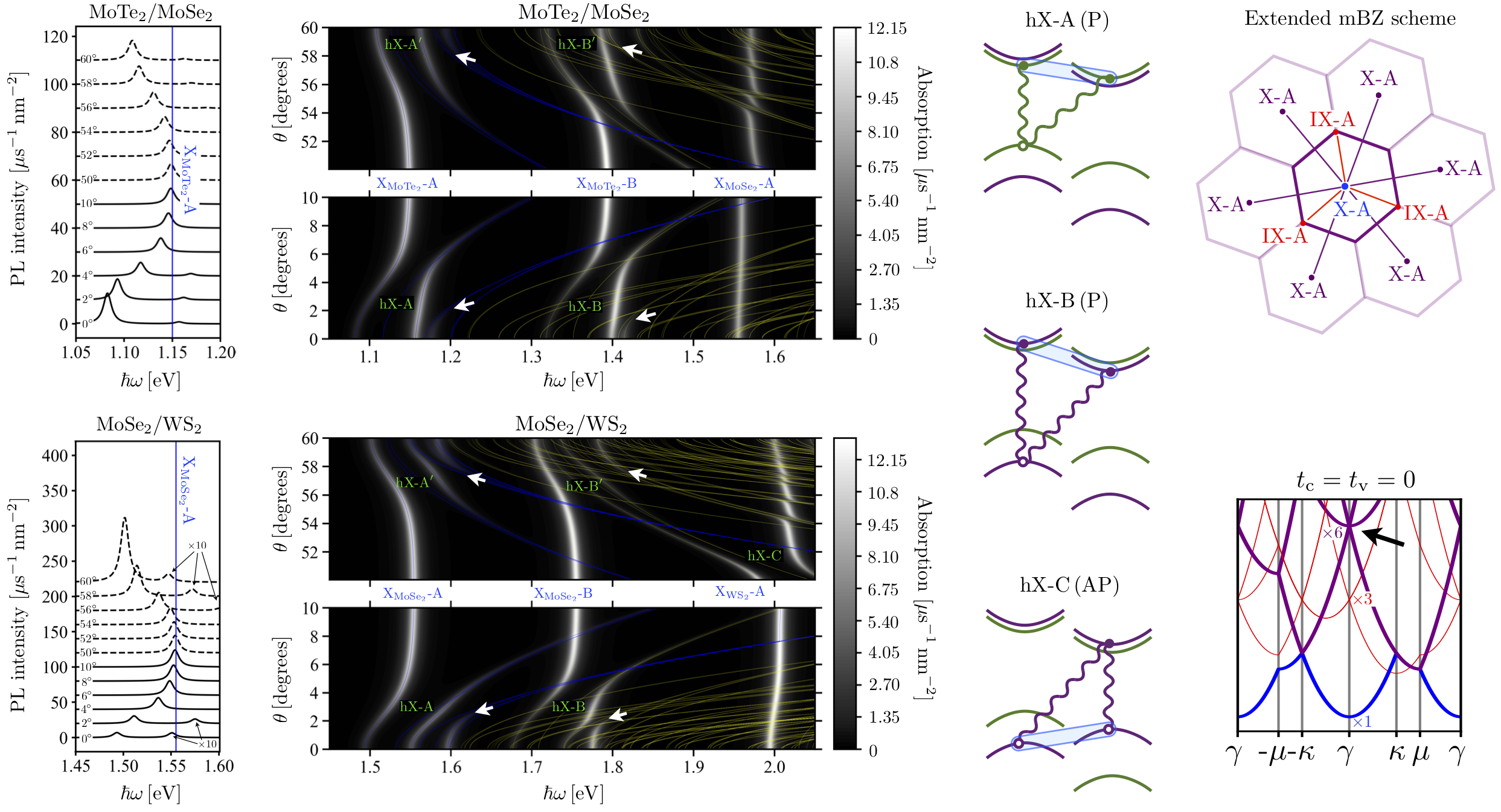
Also, we study the interplay between resonant hybridization of intra- and interlayer excitons and moiré superlattices in MoSe2/WS2 and MoTe2/MoSe2 heterobilayers, leading to the formation of hybridized excitons (hX) containing strongly mixed electron or hole states involved in the formation of intralayer (X) and interlayer (IX) excitons. Our estimates for the X and IX binding energies indicate that the weaker binding of the latter, due to the additional electron and hole out-of-plane separation, can significantly enhance the resonant condition between the two exciton species. We show that the optical spectra of hXs are dominated by their bright intralayer exciton component, resulting in identical selection rules as intralayer excitons in monolayer TMDs, in stark contrast to earlier predictions for IXs in non-resonant TMD heterostructures Tong et al. (2016); Yu et al. (2017). We present an analysis of the optical spectra of both resonant and non-resonant heterobilayers, compared in Fig. 2. In the former case, we find that the energy and state composition of optically-active hybridized excitons varies sharply with interlayer orientation, producing a strong modulation of the corresponding absorption signatures with twist angle, marked with green arrows in Fig. 2. For closely aligned resonant heterobilayers, the optical spectrum also displays a bright absorption line at higher energies enabled by moiré umklapp processes (white arrows in Fig. 2), which fold finite-momentum exciton states onto zero momentum, allowing them to acquire a finite oscillator strength and providing direct experimental evidence for mSL minibands for the excitons in the system. These signatures are absent in closely aligned non-resonant heterobilayers, where the low-energy optical features correspond to IXs (red arrows in Fig. 2) that only mix weakly with the bright intralayer exciton states. Finally, we show that hXs are sensitive to out-of-plane electric fields, due to their large IX components, and argue that vertical electrical bias can be used to tune the strength of mSL effects on excitons in TMD heterostructures.

For this purpose, in Sec. II, we introduce a general interlayer hybridization model for twisted TMD heterobilayers, parameterized using currently available ab initio parameters of monolayer TMDs (Table 3). In Sec. III, we derive an effective low-energy Hamiltonian that incorporates moiré superlattice effects in terms of harmonic potentials specific to each of the monolayer bandsWu et al. (2017); Yu et al. (2017); Wu et al. (2018b, a), which we find are applicable to TMD heterostructures with large band-edge offsets, such as MoSe2/MoS2 bilayers. We discuss the shortcomings of this harmonic potential approach, and show that it breaks down in the case of resonant hybridization. In Sec. IV, we study the opposite limit of perfect interlayer band-edge degeneracy in TMD homobilayers, and present results for their band structure features, such as the nature of the conduction-band edges and the appearance of van Hove singularities in the conduction bands. In Sec. V, we discuss two cases of TMD heterobilayers with nearly resonant band edges, namely, MoTe2/MoSe2 and MoSe2/WS2, and show that they constitute an intermediate case between typical TMD hetero- and homobilayers, which are exactly in the resonant hybridization regime. In Sec. VI, we study the effects of strong interlayer hybridization on the band structures of excitons in such heterostructures based on reported experimental values for the intralayer and interlayer exciton energies, and present theoretical predictions for the full optical spectra MoTe2/MoSe2, MoSe2/WS2, MoSe2/MoS2 and WSe2/MoS2 as functions of the interlayer alignment angle , and electric field strength.
II Model
We describe electronic states in a TMD heterobilayer in terms of the monolayer conduction- and valence-band theory near the band edges of its two constituent layers. The band edges of the bottom layer, to which the highest valence band belongs, are located at the valleys of its Brillouin zone, (). We set , according to the lattice vectors and , where is the corresponding lattice constant. Similarly, for the top layer, , containing the lowest conduction band, the band edges appear at the valleys of the Brillouin zone . Because of the lattice mismatch,
| (1) |
and the relative twist angle between the two crystals (Fig. 1, bottom), the valley momenta are related by , where represents counterclockwise rotation by an angle about the -axis. Henceforth, -layer variables are identified with a prime, and heterobilayers are labeled as . We will discuss two inequivalent stacking types: parallel (P) stacking, for twist angles ; and anti-parallel (AP) stacking, for . The two configurations are shown in Figs. 1 and 3, and any twist angle outside the range is related to one of these two stacking types by rotations or mirror reflection.111An alternative nomenclature is used, e.g., in Refs. Tong et al., 2016; Wang et al., 2017a, where P and AP stacking configurations are referred to as R and H stacking, respectively. We choose the former convention to avoid confusion with standard nomenclature for commensurate stacking..
Locally, the exact heterostructure stacking is determined by , , and a unit-cell vector , representing the shortest in-plane shift between transition metal atoms of the two layers, as illustrated in Fig. 1. For small twist angle and/or lattice mismatch, a superlattice structure emerges, known as a moiré patternKuwabara et al. (1990); Zhang et al. (2017), where the stacking determined by , set to relate positions of and atoms, is approximately preserved locally at the origin, and periodically along the heterostructure’s surface, as shown in Fig. 3. Moreover, the interlayer registry varies inside the superlattice unit cell, producing two additional regions of approximately commensurate stacking, corresponding to local values of different than that at the origin. As an example, Fig. 3 shows the case of , where the sequence of locally commensurate regions in the moiré unit cell is AA, BA and AB for P stacking; and 2H, AA’ and BB’ for AP stackingConstantinescu et al. (2013); He et al. (2014), contrasting the two stacking types. The local values for these commensurate stacking types are shown in Table 1.

The heterobilayer Hamiltonian has the general form
| (2) |
where
| (3) |
Here, the operators and [ and ], annihilate electrons of spin quantum number and wave vector () in the conduction and valence bands of the () layer. Setting the energy reference at the highest valence-band edge, the conduction and valence band dispersions can be approximated as
| (4) |
where is the heterostructure band gap; and are the interlayer conduction and valence band edge detunings; is the spin-orbit splitting of band ; and are effective masses. These model parameters, illustrated in Fig. 1 and presented in Table 3, are based on DFTKormányos et al. (2015); Kylänpää and Komsa (2015); Xu et al. (2018) and Gong et al. (2013); Cheiwchanchamnangij and Lambrecht (2012) calculations recently reported in the literature.
| P-stacking | AP-stacking | |
|---|---|---|
| AA | ||
| AB | ||
| BA |
The matrix elements for interlayer tunneling between the conduction- () or valence-bands () have the general form
| (5) |
where is the tunneling Hamiltonian, and are the numbers of unit cells in the MX2 and M’X’2 layers, and is a Wannier function centered at atomic site . In the two-center approximation, the atomic matrix element can be Fourier transformed as
| (6) |
which after substitution into (5) gives in the form
| (7) |
with interlayer hopping termsWang et al. (2017a)
| (8) |
Here, and are the reciprocal lattice vectors of the and layers, respectively, and gives the interlayer valley mismatch. As described in Ref. Wang et al., 2017a, the interlayer tunneling functions and are constrained, respectively, by the angular momentum quantum numbers of the conduction and valence bands at the and valleys. Because the conduction-band states near the valleys are formed by in-plane-isotropic orbitalsKormányos et al. (2015), for both valleys we have . By contrast, the valence-band states at the valley consist of orbitals, with . Therefore, under rotations we obtain
| (9) |
To a good approximationWang et al. (2017a), we can set
| (10) |
where represents rotation by . Thus, we may define
| (11) |
The approximation (10) truncates the sum in Eq. (8) to include only , and the two Bragg vectors
| (12) |
which connect the three equivalent valleys. These reciprocal lattice vectors are shown with black arrows in the bottom panel of Fig. 1. At this point, the stacking type (P or AP) must be specified to determine which -layer Bragg vectors give the dominant interlayer hopping terms. For closely aligned P-stacked structures, the Kronecker delta in Eq. (8) couples states near the band edges only if , and for -layer Bragg vectors (red arrows in Fig. 1, bottom)
| (13) |
One can verify that, for these specific Bragg vectors, the generalized umklapp condition in Eq. (8) becomes , where , and we have defined
| (14) |
Alternatively, for AP stacking, we must set , indicating that tunneling takes place between opposite valleys of the electron and hole layers, which are closely aligned in reciprocal space for this range of twist angles. The relevant -layer Bragg vectors in this case are
| (15) |
leading to , with
| (16) |
This leads to the simplified hopping terms
| (17) |
Equation (17) allows us to determine how the different locally commensurate regions shown in Fig. 3 contribute to interlayer carrier tunneling. Exactly at the valley (), and neglecting the lattice mismatch within each region (), we write
| (18) |
Table 2 summarizes the results of Eq. (18) for the various locally commensurate regions of the moiré superlattice, obtained by substituting the appropriate values of Table 1. For P-stacked (AP-stacked) TMD heterostructures, conduction-band tunneling takes place in AA (AA’) regions, whereas valence-band tunneling occurs in AA (2H) regionsTong et al. (2016); Kormányos et al. (2018). This result was first presented in Ref. Tong et al., 2016, where it was also reported that the parameter is somewhat larger for AP stacking, and for both stacking types, based on DFT calculations. In addition, it was shown that matrix elements and exist, representing electron hopping between the conduction and valence bands of different layers, which are significantly smaller than . As the latter couple states separated by energies comparable to the heterostructure’s band gap, we neglect them in the following. Below, we assume this hierarchy for the interlayer hopping elements, setting , based on recent experiments on MoSe2/WS2 heterobilayersAlexeev et al. (2019), and . We use these values for all materials discussed, for the purpose of obtaining a general qualitative description of TMD heterobilayers, keeping in mind that these matrix elements are material-dependent.
| P-stacking | ||
|---|---|---|
| AA | ||
| AB | ||
| BA |
| AP-stacking | ||
|---|---|---|
| AA’ | ||
| BB’ | ||
| 2H |
With Eq. (17), periodically mixes electronic states of the two layers, whose wave vectors are separated by , where runs cyclically through (Fig. 1, bottom). Note that and can be interpreted as the primitive vectors of the reciprocal lattice dual to the real-space moiré pattern shown in Fig. 3, and define the mini Brillouin zone (mBZ) presented in Fig. 1. Defining the reciprocal vectors , with and integers, the electron- and hole-layer dispersions can be folded into the mBZ to form a series of minibands with operators ()
| (19) |
which couple according to Eq. (17) to produce what we henceforth call a moiré band structure. Then, the th conduction and valence moiré bands have operators given by the linear combinations of the folded band operators,
| (20) |
where for P and AP stacking, respectively. In addition to the valley mismatch , the spin-dependent amplitudes and depend on the spin ordering of the monolayer bands. Fig. 3 shows that the detuning between the highest spin-polarized MX2 valence band and the M’X’2 valence band of the same spin increases dramatically (by hundreds of meV) from P to AP stacking, consequence of the large intralayer valence-band spin-orbit splittings (see Table 3). This leads to strong or weak interlayer valence-band mixing for P or AP stacking, respectively, leading to qualitatively different behaviors in the two stacking limits (see for example Figs. 7 and 8). This is not the case for the spin-polarized conduction bands, for which the spin-orbit splittings are much weaker, of only tens of meV.
Having defined the hybridization model (2), in the following Sections we study two important limit cases for the interlayer band alignment. First, in Sec. III we look at MoSe2/MoS2 as a typical example of type-II semiconducting TMD heterostructures, with large band offsets . Then, in Sec. IV, we study the opposite limit of , choosing bilayer MoSe2 as a case study.
| [eV] | [eV] | [eV] | [meV] | [meV] | ||||||||||||||||
|---|---|---|---|---|---|---|---|---|---|---|---|---|---|---|---|---|---|---|---|---|
| [meV] | [meV] | |||||||||||||||||||
| BL-MoSe2 | 1. | 330a | 0. | 0 | 0. | 0 | 11. | 0b | 11. | 0b | 0. | 38c | 0. | 38d | 2. | 20f | 3. | 289b | 3. | 289b |
| 93. | 0b | 93. | 0b | 0. | 44c | 0. | 44d | 2. | 20f | 6. | 463g | |||||||||
| MoSe2/MoS2 | 0. | 960a | 0. | 630a | 0. | 370a | 11. | 0b | 1. | 5b | 0. | 38c | 0. | 35d | 2. | 20f | 3. | 289b | 3. | 157b |
| 93. | 0b | 74. | 0b | 0. | 44c | 0. | 43d | 2. | 22f | 6. | 972f | |||||||||
| MoTe2/MoSe2 | 0. | 860a | 0. | 470a | 0. | 070a | 18. | 0b | 11. | 0b | 0. | 69e | 0. | 38c | 2. | 16f | 3. | 516b | 3. | 289b |
| 109. | 5b | 93. | 0b | 0. | 66e | 0. | 44c | 2. | 20f | 7. | 421f | |||||||||
| MoSe2/WS2 | 1. | 270a | 0. | 270a | 0. | 060a | 11. | 0b | -16. | 0b | 0. | 38c | 0. | 27c | 2. | 20f | 3. | 289b | 3. | 16b |
| 93. | 0b | 241. | 5b | 0. | 44c | 0. | 32c | 2. | 59f | 6. | 913f | |||||||||
III Perturbation theory for non-resonant interlayer hybridization and harmonic potential approximation for moiré superlattices
The importance of interlayer hybridization depends crucially on the ratio between the interlayer tunneling matrix elements and the band edge detunings . When these ratios are small, one can treat perturbatively, in terms of the -dependent energy corrections produced by the tunneling processes, which in real space form a periodic potentialKindermann et al. (2012); Wallbank et al. (2013). This approach to describing the effects of a moiré superlattice on the electronic states has been used in Ref. Wu et al., 2018a, and for excitons in Refs. Wu et al., 2017; Yu et al., 2017; Wu et al., 2018b, where the potential was estimated from ab initio calculations. In this section, we derive the tunneling contribution to this potential from the microscopic Hamiltonian (2), based on a perturbative treatment of the elementary excitations in the heterobilayer (conduction-band electrons and valence-band holes). For clarity, the final result is presented in terms of the conduction- and valence-band dispersions.
We apply the unitary transformation to the Hamiltonian (2), with an anti-Hermitian operator. The resulting rotated Hamiltonian is given to second order in as
| (21) |
We eliminate to first order by choosingSchrieffer and Wolff (1966) , and keep only terms up to second order in to get the effective model . The first term corresponds to Eq. (3), with the renormalized dispersions
| (22) |
whereas the second term gives ()
| (23) |
represents scattering of electrons and holes by moiré vectors , produced by two sequential interlayer tunneling processes. Fig. 4(a) shows an electron near the valley of band tunnel into band through one of the processes depicted in the botom panel of Fig. 1, followed by a second tunneling process back into band . The net result is a scattering process of the initial state by a moiré Bragg vector . An inverse Fourier transform of Eq. (23), taking in the dispersions, gives simple real-space harmonic potentials for each of the bands, of the form ()
| (24) |
This is the same type of harmonic potential, as used in Refs. Wu et al., 2017; Yu et al., 2017; Wu et al., 2018b, a for both carriers and excitons in TMD heterobilayers. Whereas in those cases the coefficients were determined by fitting to the spatial variation of the heterostructure band gap, as determined by DFT calculations, in our analysis they are determined from a microscopic model. We point out, however, that our approach is based purely on interlayer tunneling, and neglects lattice relaxation in the regions of commensurate stacking.

Whether Eqs. (24) constitute a valid low-energy theory for carriers near the band edges in a heterostructure with twist angle depends on the band alignment. To illustrate this, we take the first term of Eq. (23) near the valley (), and note the divergence when . As shown in Fig. 4(b), this is due to a crossing of the two conduction bands, which can occur at or near the bottom of the higher-energy band for some values of . The resulting strong interlayer mixing of electronic states near the higher band edge leads to the breakdown of perturbation theory. Turning to band , the third term in Eq. (23) does not show a divergence, reflecting the fact that a higher parabolic band can never cross the bottom of a lower one. This, however, does not guarantee the validity of the harmonic-potential approximation. To make this statement precise, we define perturbative parameters
| (25) |
for each band, where and are determined by the twist angle, as discussed in Sec. II: for P stacking, and for AP stacking. The effective potential (24) correctly describes low-energy carriers in valley of band when , and interlayer band mixing is weak. This condition may not be met if the interlayer detunings or are small, as illustrated in Fig. 4(b).

Using MoSe2/MoS2 as an example, we take ab initioGong et al. (2013); Xu et al. (2018) results for the monolayer band parameters (Table 3). The perturbative parameters plotted in Fig. 5(a) as functions of the twist angle suggest that the harmonic-potential picture holds for angles and . Although the small-twist-angle approximations leading to Eqs. (13) and (15) are not applicable for , Fig. 5(a) shows that all perturbative parameters are negligible for large twist angles, and interlayer tunneling effects can be neglected, as expected for strongly misaligned heterobilayers. Thus, our model can be applied safely for . We numerically diagonalized both the full hybridization Hamiltonian (2), and the harmonic-potential effective model (24), using a large basis of moiré bands Wallbank et al. (2015). Dispersions with valley quantum number near the main conduction and valence band edges are shown in Figs. 5(b) and 5(c), for P- and AP-stacked configurations, respectively, along the mBZ path defined in Fig. 1. Their counterparts can be obtained by time-reversal symmetry, and are not explicitly shown. The figures show quantitative agreement between the full Hamiltonian and the harmonic approximation near the band edges for MoSe2/MoS2. A shortcoming of the model (25) is visible in the valence bands, however, where the avoided crossings at are not captured by the harmonic approximation, and instead a Dirac cone appears. This crossing is not accidental, but exact; it appears for all material pairs (see Figs. 11-14), and can be understood as follows: the three lowest minibands, with indices , and , become degenerate at the -points, as sketched in Fig. 4(c). Evaluating the corresponding coefficients, given by the second term of Eq. (23), we find that the three minibands couple through the -symmetric Hamiltonian
| (26) |
where
| (27) |
The resulting eigenvalues are , and a doubly degenerate level , responsible for the spurious level crossing. By comparison, the harmonic potentials proposed in Refs. Wu et al., 2017; Yu et al., 2017; Wu et al., 2018b, a give the simpler but less symmetric form
with eigenvalues and , which allow a gap opening at .
IV Resonant interlayer hybridization in twisted TMD homobilayers

Whereas the large band-edge offsets and guarantee the validity of the harmonic-potential model for most TMD heterobilayers, the opposite limit of can be found in TMD (homo)bilayers. Fig. 6 shows that the perturbative parameters for twisted bilayer MoSe2 are small only for strongly misaligned configurations (), whereas for close alignment or anti-alignment, interlayer hybridization cannot be treated as a perturbation.
We present the band structures of P- and AP-stacked bilayer MoSe2 in Figs. 7 and 8, respectively. We point out that, in the case of homobilayers, a more symmetric mBZ can be defined by shifting our chosen mBZ (Fig. 1) by . This transforms and , up to a moiré Bragg vector, corresponding to the convention followed in, e.g., Refs. Wallbank et al., 2015; Koshino and Moon, 2015. Here, however, we will use the mBZ convention of Fig. 1, for the sake of consistency. To show the degree of interlayer state mixing, we color-code the plot symbols in Figs. 7(a) and 8(a), according to the expectation value of the out-of-plane electric polarization, given by [see Eq. (20)]
| (28) |
for each moiré band, at every wave vector . In Eq. (28), we have assumed, without loss of generality, that the () layer is at the top (bottom) of the heterostructure; is the elementary charge, and is the interlayer distance (see Table 3). The polarizations take values from (blue) to (red), in units of , for electron states fully localized in the and layer, respectively. These values correspond to the state’s out-of-plane electric dipole moment, measured with respect to the central plane of the stack.

Figs. 7(a) and 8(a) show weak polarization of the electronic states in several regions of mBZ, indicating an even spatial distribution in the out-of-plane direction between the two MoSe2 layers, caused by the strong interlayer mixing. The highest valence states in the case of AP stacking are the exception, however, as seen in the bottom panel of Fig. 8(b). This is because, as illustrated in the right panel of Fig. 6, in AP-type bilayers the interlayer tunneling takes place between states of opposite valley quantum number (), which due to spin-valley locking in the monolayersXiao et al. (2012), have opposite ordering of the spin-polarized bands. Therefore, bands of same spin quantum number in opposite layers are separated by a large spin-orbit splitting, typical of TMD valence bands (see Table 3), and hybridize only weakly.
For the lowest conduction bands, however, a modest spin-orbit coupling strength of order allows for strong interlayer hybridization also in the case of AP stacking (Fig. 6, right), producing stark qualitative differences between moiré band structures for P- and AP-MoSe2 bilayers, seen in the top panels of Figs. 7(a) and 8(a). For P-type bilayers, the lowest conduction bands of a given valley have the same spin quantum number in both monolayers, and mix to form the moiré band edge shown in Fig. 7(a). The miniband edge has two branches, located at mBZ points and , which belong to the same spin-polarized mixed miniband, and are separated only by a shallow saddle point, which produces a van Hove singularity close to the band edge, as shown in Fig. 7(b). For AP-type bilayers, the two branches of the conduction-band edge belong to minibands of opposite spin quantum number, as shown in Fig. 8(a). Note that above each band minimum at or , the opposite-spin miniband flattens significantly, producing the van Hove singularity shown in Fig. 8(b).
V Interlayer hybridization and moiré superlattice minibands for electrons in and
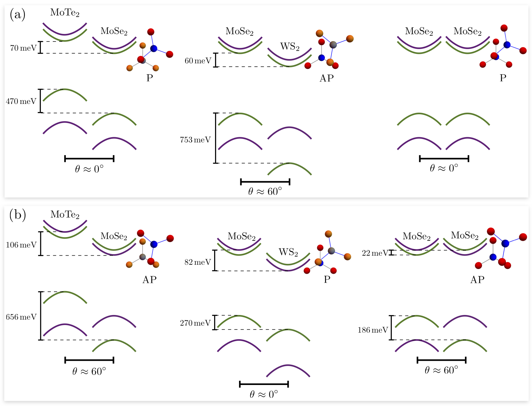
In this Section we discuss TMD heterobilayers in which the interlayer band alignment produces accidental near-resonant hybridization between either the conduction- or valence-band edges of the two constituting TMD layers. This situation has been predictedGong et al. (2013); Kozawa et al. (2016); Xu et al. (2018) for the conduction bands of MoSe2/WS2 heterostructures, and recently confirmed by photoluminescence experimentsAlexeev et al. (2019). Moreover, first principles estimates based on calculationsGong et al. (2013) also point toward near-resonant conduction bands in MoTe2/MoSe2 (see Table 3 and Fig. 10). Similarly to the case of TMD homobilayers, for this class of heterostructures, the harmonic-potential approximation breaks down precisely for closely aligned and anti-aligned configurations, where effects of the moiré superlattice are most prominent. This is shown by the perturbative parameters presented in Fig. 9, which indicate that, for and , it is necessary to treat the interlayer tunneling term (7) exactly, due to near-resonant interlayer hybridization at the conduction-band edges.

V.1 P-stacked
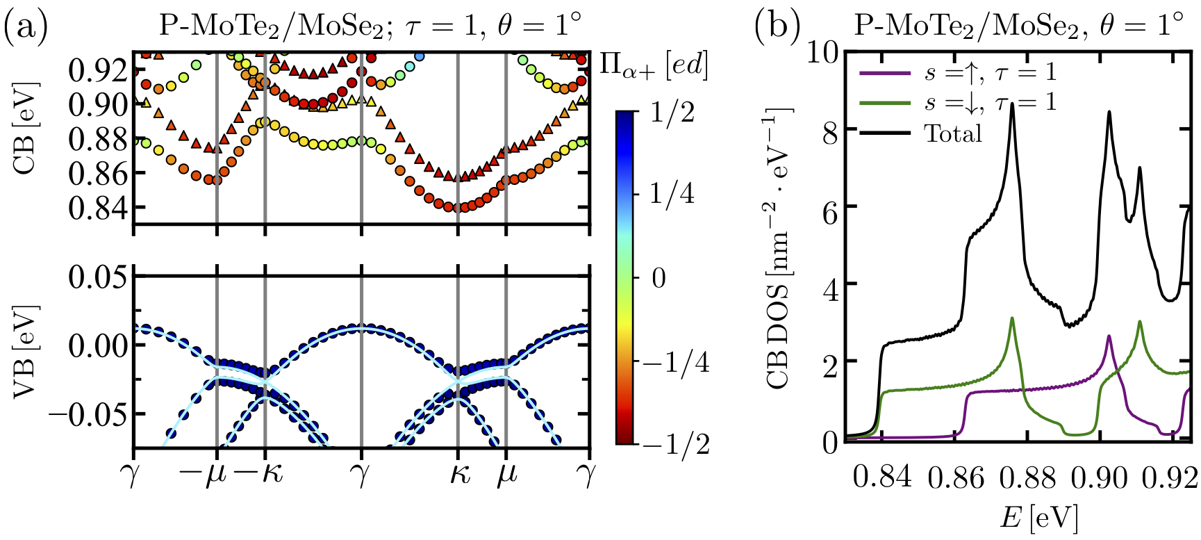
Fig. 10(a) sketches the atomic arrangement and interlayer band alignment of P-stacked twisted MoTe2/MoSe2. The corresponding moiré conduction and valence miniband structures for are presented in Fig. 11(a), as obtained by direct diagonalization of the full Hamiltonian (2). All bands shown have valley quantum number , and the bands can be obtained by a time reversal transformation. As expected from Fig. 10(a), we find that P-MoTe2/MoSe2 is an indirect-band-gap semiconductor, with the valence and conduction band edges located at the and points. However, note that, whereas the highest valence bands are well localized in the main hole layer, similarly to the case of MoSe2/MoS2 [Fig. 5(b)], the lowest conduction bands show significant depolarization across the mBZ. This is due to the strong interlayer mixing caused by the relatively small detuning of between hybridizing band edges, which distributes the miniband states between the two layers, similarly to the case of P-type TMD homobilayers [Fig. 7(a)]. Moreover, a comparison between the conduction-miniband density of states of P-MoTe2/MoSe2 and of P-type bilayer MoSe2 [Figs. 11(b) and 7(b)] shows important parallels between the two cases; in particular, the formation of two van Hove singularities above the band edge.
V.2 AP-stacked
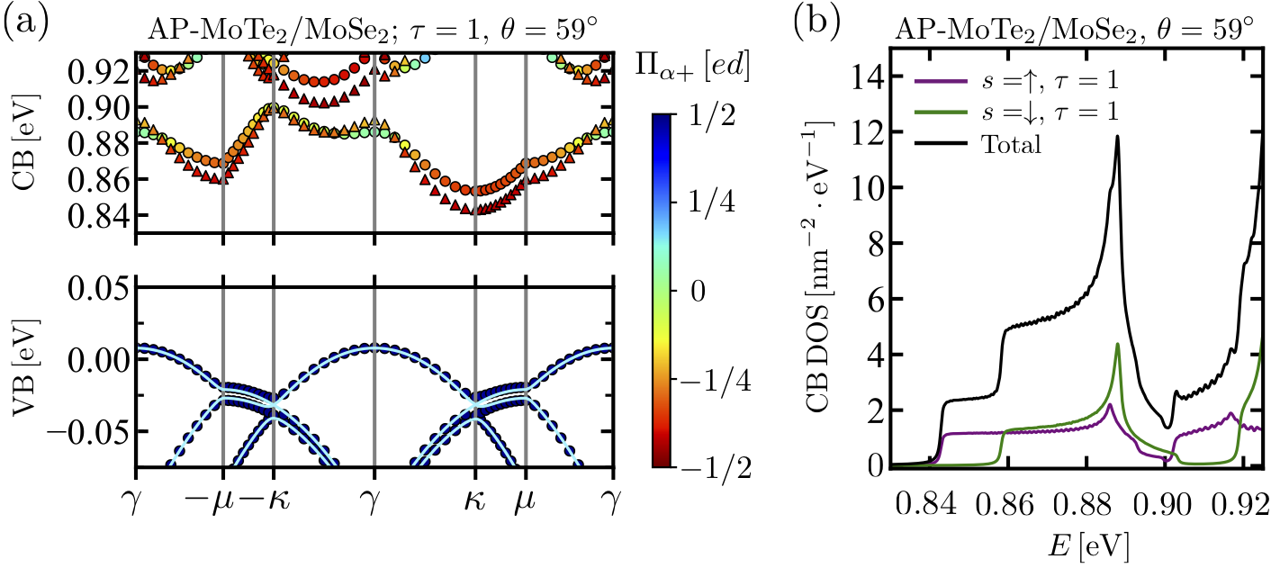
Fig. 10(b) shows the band alignment of AP-stacked MoTe2/MoSe2, where states near the MoTe2 valley hybridize with those at the MoSe2 valley, which have the opposite spin ordering in both the conduction and valence bands. The corresponding moiré miniband structure, for twist angle , is shown in Fig. 12(a), and the conduction-miniband density of states is presented in Fig. 12(b). As in the case of P stacking, for AP stacking we find an indirect gap semiconductor, whose highest valence bands are largely confined to the MoTe2 layer, whereas the conduction minibands show different degrees of interlayer mixing throughout the mBZ. The conduction-band alignment in this case is more closely related to AP TMD homobilayers (Fig. 8), due to the opposite spin ordering of the bands, which somewhat diminishes resonant hybridization of the band edges. Similar qualitative features are apparent in the density of states [Figs. 8(b) and 12(b)], which show a single van Hove singularity near the band edge.
V.3 P-stacked
MoSe2/WS2 heterostructures are different from all the cases discussed so far, due to the presence of different transition metal atoms in the two TMD layers. In particular, tungsten-based TMDs are knownKormányos et al. (2015) to display a negative spin-orbit coupling constant for the conduction band, as opposed to the positive one found in molybdenum-based TMDs (see Table 3). This results in opposite ordering of the spin-polarized conduction bands of MoSe2 and WS2 in a P-MoSe2/WS2 heterostructure, as illustrated in Fig. 10(b)—an analogous situation to AP-type homobilayers.
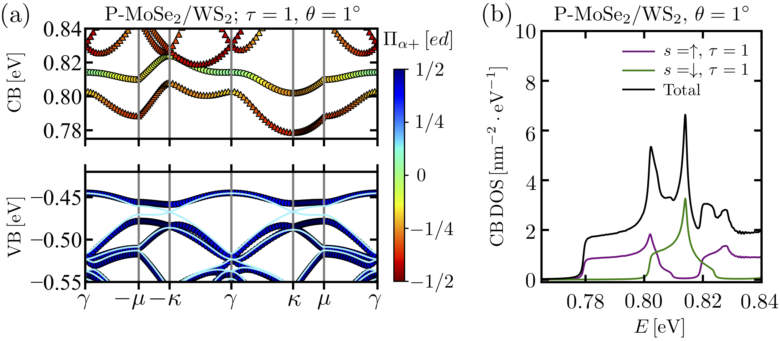
Fig. 13(a) shows the moiré band structure of P-MoSe2/WS2 at twist angle , with the density of states corresponding to the conduction band shown in Fig. 13(b). Notice the strong electric dipole moment imbalance between the spin-up and spin-down conduction bands, indicated by the symbol colors in Fig. 13(a). This strong spin asymmetry is caused by the combination of opposite spin splittings of the monolayer conduction bands, and the small interlayer offset , which produces almost perfect alignment between the () spin-down band edges () and a much larger detuning of the spin-up bands (), as illustrated in Fig. 10(b). This leads to different levels of interlayer mixing for the two spin-polarized minibands.
V.4 AP-stacked
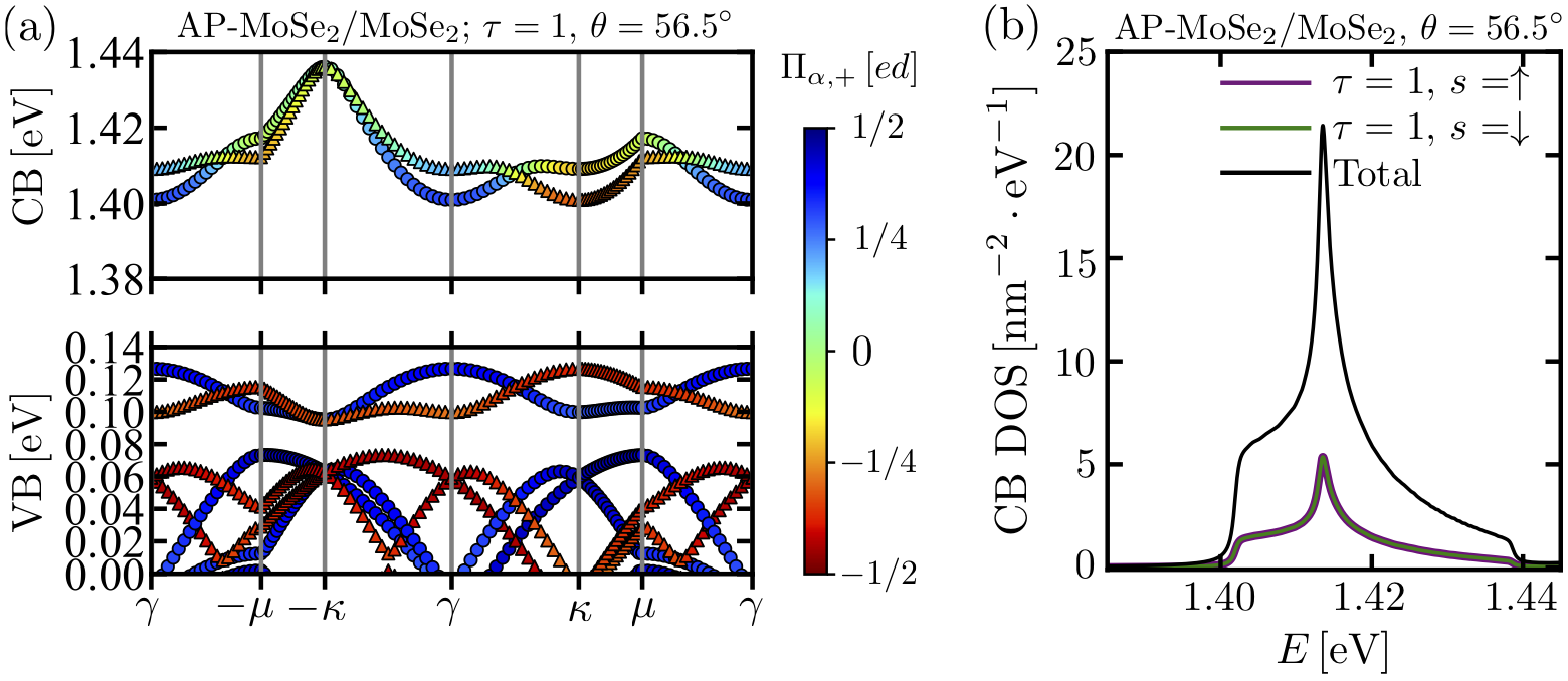
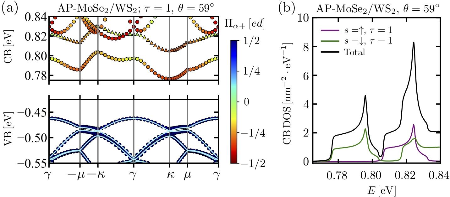
Finally, Fig. 14 shows the moiré band structure and conduction-miniband DOS for AP-type MoSe2/WS2 at twist angle , corresponding to the schematic shown in Fig. 10(a). For this range of angles, where MoSe2 valley states hybridize with WS2 states of valley quantum number , both layers show the same spin ordering in the conduction bands, and the situation is qualitatively similar to the case of P-type homobilayers. Some similarities between the two cases can be found in Fig. 14, such as the spin polarization of the bottom band across the mBZ, and a rough two-peak structure in the density of states near the conduction-band edge, reminiscent of the van Hove singularities shown in Fig. 7(b).
V.5 Electrical control of moiré superlattice effects
The band structure calculations presented in Figs. 11–14 show that P- and AP-type MoTe2/MoSe2 and MoSe2/WS2 heterostructures are type II semiconductors, with a – indirect band gap. However, it is possible to reduce the offset between the conduction band edges by application of a positive interlayer bias voltageRivera et al. (2015); Klein et al. (2016); Wang et al. (2017b) . In fact, recent experimentsKlein et al. (2016) have demonstrated that interlayer voltages of up to approximately can be produced in TMD bilayers by means of metallic gates. The resulting potential gradient along the heterostructure’s out-of-plane axis will lower the (bottom) layer’s band while raising the (top) layer’s band, such that a suitable value of can impose a degeneracy between the two minima at and .
Figs. 15(a) and 15(b) show the conduction miniband structures of P-type MoTe2/MoSe2 and AP-type MoSe2/WS2, under the critical bias voltages that establish a band-edge degeneracy at the and points. In both cases, we find that the critical bias is twist-angle dependent, giving values of for perfectly aligned P-MoTe2/MoSe2, and a lower value of for twist angle . Note that both of these values correspond to energies greater than the band offset of , indicated in Fig. 10(a). The same trend is found for AP-MoSe2/WS2, where the critical bias for perfect anti-alignment () is , compared to for , and to the offset shown in Fig. 10(a). The lowest conduction minibands shown in Fig. 15 bear striking resemblance to those of P-type TMD homobilayers (Fig. 7), with two branches of the band edge at the and points belonging to the same spin-polarized band, and a van Hove singularity forming just above the band edge.
Similarly, Figs. 16(a) and 16(b) show the corresponding cases of critical interlayer bias for AP-MoTe2/MoSe2 and P-MoSe2/WS2, both for perfect (anti) alignment and for a finite misalignment angle, showing also a weak twist-angle dependence of the critical bias voltage. The conduction minibands in these cases show direct correspondence to those of AP-type TMD homobilayers (Fig. 8), with the - and -point branches of the band edge belonging to bands of opposite spin polarization, and a flattening of the second conduction miniband above each minimum that is particularly clear in P-MoSe2/WS2, as a result of the similar effective electron masses of the two layers (Table 3).
In the case of TMD homobilayers, the band-edge degeneracy at the and points is a direct consequence of the identical dispersions of the two layers, as well as the perfect band alignment in the case of P stacking. However, note that this is not the case for P- or AP-type MoTe2/MoSe2 and MoSe2/WS2, since the predicted critical are twist-angle dependent, and can, in fact, be larger than the actual offsets between the hybridizing bands. The reason behind this discrepancy is the asymmetry between the conduction-band dispersions of the two layers, parametrized by their different effective electron masses (Table 3). Thus, when these bands are folded into the mBZ, different miniband configurations are obtained at and , producing an asymmetry between the band minima at those points in the mBZ.
VI SL minibands for resonantly hybridized intra- and interlayer excitons
| 0. | 176 | 0. | 164 | 21. | 4 | 21. | 4 | |||
| WS2/MoS2 | 37.89 | 38.62 | 0. | 194 | 0. | 163 | 18. | 2 | 21. | 5 |
| 0. | 170 | 0. | 157 | 21. | 4 | 21. | 7 | |||
| WSe2/MoS2 | 45.11 | 38.62 | 0. | 183 | 0. | 158 | 18. | 9 | 21. | 7 |
| 0. | 195 | 0. | 170 | 17. | 8 | 19. | 8 | |||
| MoSe2/MoS2 | 39.79 | 38.62 | 0. | 191 | 0. | 172 | 18. | 4 | 19. | 4 |
| 0. | 196 | 0. | 162 | 17. | 7 | 21. | 5 | |||
| MoSe2/WS2 | 39.79 | 37.89 | 0. | 174 | 0. | 164 | 21. | 5 | 21. | 1 |
| 0. | 169 | 0. | 158 | 21. | 5 | 21. | 3 | |||
| WSe2/MoSe2 | 45.11 | 39.79 | 0. | 185 | 0. | 157 | 18. | 4 | 21. | 7 |
| 0. | 177 | 0. | 147 | 15. | 7 | 20. | 1 | |||
| MoTe2/MoSe2 | 73.61 | 39.79 | 0. | 152 | 0. | 151 | 20. | 9 | 18. | 9 |
Much of the current interest in the properties of TMD systems stems from their outstanding monolayer optical propertiesMak et al. (2010); Splendiani et al. (2010); Wang et al. (2018), produced by their direct band gap at the points, and dominated by the formation of strongly-bound 2D intralayer excitons (X). By contrast, in twisted TMD heterobilayers such as those discussed in Secs. III to V, the ground-state excitons are formed by electron and hole states confined to opposite layers, known as interlayer excitons (IXs)Rivera et al. (2015); Heo et al. (2015); Nayak et al. (2017); Zhu et al. (2017). The wave vector mismatch between the electron and hole band edges shown in, e.g., Fig. 5, means that the center-of-mass momentum of low-energy IXs is finite, and energy-momentum conservation forbids radiative recombination, unless mediated by some compensating mechanism, such as phonon or impurity scattering. In other words, the lowest-energy IX is momentum-dark.
Until recentlyAlexeev et al. (2019), Xs and IXs have been mostly discussed as independent objects; however, it is clear that the band hybridization effects predicted in Secs. IV and V must lead to mixing of IX and X statesDeilmann and Thygesen (2018). Indeed, as the (positive) binding energy of IXs is smaller than that of Xs, , due to the additional out-of-plane distance between the electron and hole, the detuning between the lowest X and IX energies must be approximately , which improves the resonant condition. To show this, we estimate the binding energies of all possible species of X and IX for different TMD heterobilayers, by solving the two-body problem for electrons and holes using the finite elements method, considering the Keldysh-typeKeldysh (1979) long-range intra- and interlayer interactions
| (29) |
derived in Ref. Danovich et al., 2018. The results are presented in Table 4. In Eq. (29), represents momentum transfer; is the interlayer distance; () is the screening length of layer (), with () the in-plane dielectric susceptibility, and is the average dielectric constant of the environment. The corresponding exciton Bohr radii were estimated as the RMS width of the numerically obtained lowest bound-state wave function, which is of type. From Tables 3 and 4, we can see that the difference in binding energies of the intra- and interlayer excitons, , is comparable to for materials with near-resonant band edges, such as MoTe2/MoSe2 and MoSe2/WS2. This leads to enhanced hybridization between these Xs and IXs, as compared to electrons and holes, resulting in hybridized excitons (hXs) formed by resonantly mixed X and IX states. As we show below, similar resonant conditions can arise also for higher-energy intra- and interlayer excitons, such that signatures of hXs can appear all throughout the optical spectra of TMD heterobilayers. These strongly mixed states have a large intralayer component that allows them to recombine radiatively, making hXs semi-bright, whereas the out-of-plane electric dipole moment, inherited from their interlayer component, makes hXs sensitive to the electrostatic environment of the heterobilayer, through the Stark effect.
Consider the X states of and , and all possible IX states of the heterobilayer, given respectively byMoskalenko and Snoke (2000); Yu et al. (2015)
| (30) |
In each case, the exciton center-of-mass momentum is represented by ; , , and are the corresponding electron-hole relative motion wave functions in reciprocal space; is the neutral ground state of the heterobilayer in the absence of interactions; and is the heterostructure’s surface area. The Xs and IXs have parabolic dispersions given by
| (31) |
We will focus on intravalley X and states, formed by electrons and holes that can recombine in the absence of intervalley scattering. For IX and , we consider only the set of low-energy states that can hybridize with intravalley X and according to Eq. (17), such that we must set for P or AP stacking, respectively. We further assume that no spin scattering mechanisms are present in the system, and excitons can recombine only if its constituting electron and hole have opposite spin quantum numbers. We call such excitons spin-bright, and in the opposite case, the exciton is called spin-dark. The eight spin-bright exciton species are represented schematically in Fig. 17 for the case of P-MoSe2/WS2, and the intralayer exciton states are labeled according to the usual nomenclature of A and B excitons.
In principle, the exciton energies at zero momentum can be obtained from the ab initio band alignment parameters of Table 3, together with the binding energies of Table 4, as
| (32) |
However, the former quantities depend directly on the intra- and interlayer band gaps, which may be underestimated by ab initio methods. Instead, we use experimental values available in the literature, presented in Table 5. These correspond to the A- and B-Xs of each layer, and the lowest-energy IX excitons of the heterostructure. In our present notation, these states are respectively () , and , where for P and AP stacking.
We estimate the energies of the higher states and by combining the experimental values of Table 5 with the ab initio spin-orbit splittings and conduction-band-edge offsets of Table 3, and the binding energies of Table 4. This same strategy is followed for all IXs in the case of MoTe2/MoSe2, for which no experimental results are available at the moment, using the experimental monolayer X energies in Table 6.
| A exciton energy [eV] | B exciton energy [eV] | |
|---|---|---|
| MoS2 | 1.84a | 2.00a |
| MoSe2 | 1.58a | 1.76a |
| MoTe2 | 1.10–1.20b,c,d | 1.35b, 1.44d |
| WS2 | 2.01a, 1.99e | 2.39a, 2.26e |
| WSe2 | 1.66a, 1.63e | 2.10a, 2.07e |
Similarly to carrier states, different intralayer and interlayer exciton species are mixed by the tunneling term in Eq. (2). Using the simplified form (17), we obtain the matrix elements
| (33) |
with any other matrix elements between the relevant bright excitons being equal to zero. In Eq. (33), is chosen according to Eqs. (14) and (16), and we have defined
| (34) |
with , , and the real-space relative motion wave functions, given by the inverse Fourier transforms of , , and .
The expressions in (34) can be simplified by noting that, in each case, the difference of mass ratios appearing in the argument of the first exponential is much smaller than one for the heterostructures discussed (see Table 3). Then, assuming two-dimensional -states for the X and IX wave functionsBerkelbach et al. (2013), with corresponding Bohr radii , , and , yields the momentum-independent expressions
| (35) |
Analogously to Eq. (17), Eq. (33) defines a mBZ for excitons, where X and IX states with center-of-mass momenta separated by moiré Bragg vectors mix. The resulting intralayer-interlayer hybridization model can be solved by direct diagonalization within the mBZ defined in Fig. 1.
VI.1 hX formed by IX hybridization with the interlayer A exciton
Fig. 18 shows the moiré band structures for the () X and IX states in perfectly aligned (P-type) and anti-aligned (AP-type) MoTe2/MoSe2 and MoSe2/WS2. For both material pairs, the flatness of the lowest exciton bands is a consequence of the resonant condition between the intralayer A exciton and the (detunings are approximately for MoSe2/WS2 and for MoTe2/MoSe2), combined with the reduced size of the mBZ at perfect alignment or anti-alignment. The symbol colors in Fig. 18 indicate the composition of the exciton state, with blue or red representing a large X or IX component, and intermediate colors corresponding to hXs. Note that multiple high-energy -point hXs appear in both materials, some of which are optically active and should contribute to the heterostructure’s absorption spectrum, as discussed in Figs. 19, 21 and 22.
The evolution with twist angle of the lowest bright exciton energy and state composition are shown in Figs. 18(c) and 18(d), displaying sharp variations of approximately to in both material pairs, when departs from or . For those twist angle ranges, the lowest bright exciton is hX-A, formed by resonant hybridization of an IX with the A intralayer exciton, whereas for strong misalignment angles , it is the fully bright X-A state. The slight asymmetry of the curve, especially visible for MoTe2/MoSe2 [Fig. 18(c)], is caused by the opposite conduction-band spin-orbit splitting in the valleys of the layer, resulting in different IX energies for P and AP configurations. The blue curves in Figs. 18(c) and 18(d) show the exciton activation energy as a function of twist angle, indicating what temperature is required to populate these exciton states, and produce photoluminescence. Note that for the case of MoSe2/WS2, this is always lower than room temperature (), reaching values as low as at . Based on these results, we have evaluated the photoluminescence spectra of both heterostructures (Appendix A), which we present for different twist angles in Fig. 19.
The latter Figure also shows the MoTe2/MoSe2 and MoSe2/WS2 absorption spectra for varying interlayer twist angle (Appendix B), which captures the full optical spectrum of the heterostructure. For both alignment cases, the lowest hX pair, labeled hX-A, is formed by resonant hybridization of an IX with the intralayer A exciton ( and , respectively), driven by interlayer electron hopping. The IX component of each hX-A state is formed by an electron and hole residing in different layers, and thus separated by a distance of approximately (Table 3). This IX component possesses an electric dipole moment of to (), and will couple to out-of-plane electric fields , modifying the hX energies (Stark shift) and state compositions, and ultimately splitting them into pure Xs and IXs. This is shown in Figs. 21 and 22, where we present the absorption spectra of P- and AP-type MoTe2/MoSe2 and MoSe2/WS2, respectively, for fixed twist angle and varying field strength . In each case, the IX can be easily identified within the lower-energy multiplet of lines by its Stark shift, and direct correspondence with the reference, free IX line, shown in red. X-A, on the other hand, can be identified by its lack of a Stark shift, recovering its unperturbed value at large, negative (blue line).
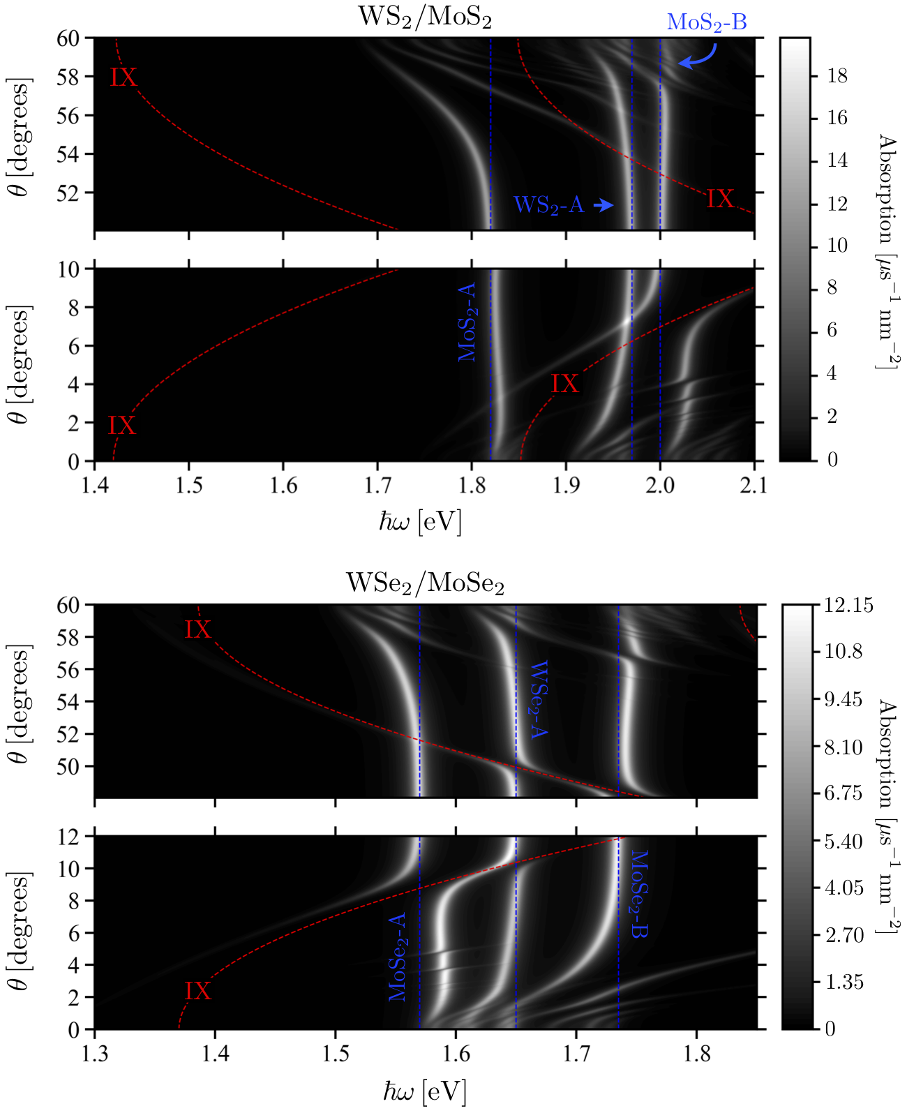
The optical spectra of hXs are dominated by their large intralayer-exciton component, leading to identical optical selection rules as the monolayersXiao et al. (2012). This is in stark contrast to IXs in TMD heterostructures with non-resonant band edges, whose optical selection rules are determined by the local stackingYu et al. (2015, 2017); Wu et al. (2018b) (see Fig. 3), and dominated by the weak interlayer tunneling matrix elements and , discussed in Sec. II. In addition to the case of MoSe2/MoS2, shown in Fig. 2, Fig. 20 shows the absorption spectra of WS2/MoS2 and WSe2/MoSe2, where intra- and interlayer excitons are strongly off resonance, as reported in Table 5. For WS2/MoS2, the lowest-energy interlayer exciton line ( for P and AP stacking, respectively) is completely absent in our approximation () due to negligible hybridization with the bright intralayer WS2-A and MoS2-A excitons. In WSe2/MoSe2, the lowest absorption peak visible corresponds to , which in our approximation gains oscillator strength only for large twist angles as it approaches the energy of the MoSe2-A exciton, even showing an avoided crossing at photon energies between and for . Note that, due to the ordering of the intralayer exciton energies in these heterobilayers, this avoided crossing is produced by interlayer hole tunneling, as opposed to electron tunneling, discussed below in the context of MoSe2/WS2 and MoTe2/MoSe2 heterostructures. Surprisingly, the intralayer exciton lines of perfectly aligned P- and AP-stacked WS2/MoS2 and WSe2/MoSe2 display intricate fine structures, corresponding to higher intralayer exciton minibands, which should be discernible at low temperatures, and appear as anomalous broadening of the intralayer exciton lines in high-temperature experiments.
VI.2 hX formed by IX hybridization with the intralayer B exciton
In addition to the sharp hX energy modulation shown in Figs. 18(c) and 18(d), the higher-energy features in the absorption spectra also reflect the formation of a secondary pair of hXs for P stacking, and two secondary pairs of hXs for AP stacking. In the former case, the pair of lines labeled hX-B originates as the intralayer B exciton () hybridizes resonantly with , through interlayer electron tunneling. This type of mixing also occurs in the latter case of AP stacking, producing the pair of lines labeled hX-B’ in Fig. 19. Surprisingly, an additional near resonance between the A exciton () and the interlayer exciton appears for relatively large misalignment angles, , giving rise to a third pair of hXs, labeled hX-C. By contrast to all previously discussed cases, hX-C are produced by interlayer tunneling of holes, as sketched in the right panels of Fig. 19. This type of mixing is possible only for AP stacking in both MoTe2/MoSe2 and MoSe2/WS2, where the top valence band of the layer and that of the have opposite spin quantum numbers. The smooth twist-angle crossover from hX-B to hX-C produces a clear absorption line that shifts with increased misalignment by a remarkable . This is enabled by the large interlayer hole tunneling matrix element , which gives strong mixing between the A exciton and even at , where the detuning between these two exciton states is relatively large. Figs. 21 and 22 show that sufficiently large, positive electric fields bring down the higher-energy states, due to their positive electric dipole moments (see Fig. 17), allowing them to also hybridize with the B exciton to produce the complex absorption signatures appearing in the top-right corner of each panel.
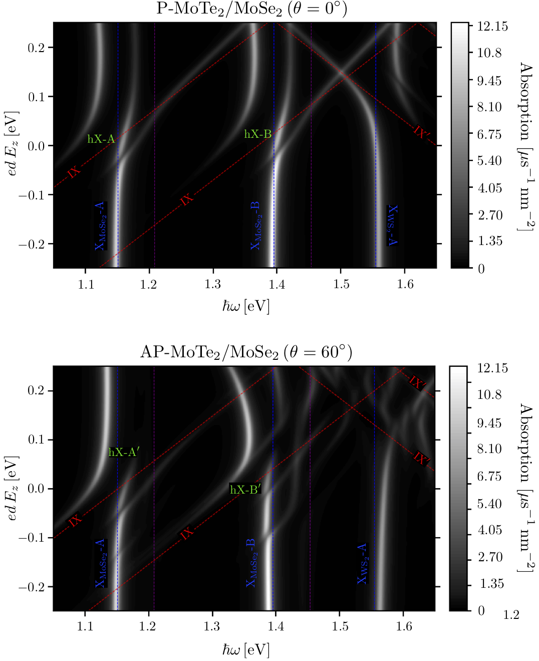
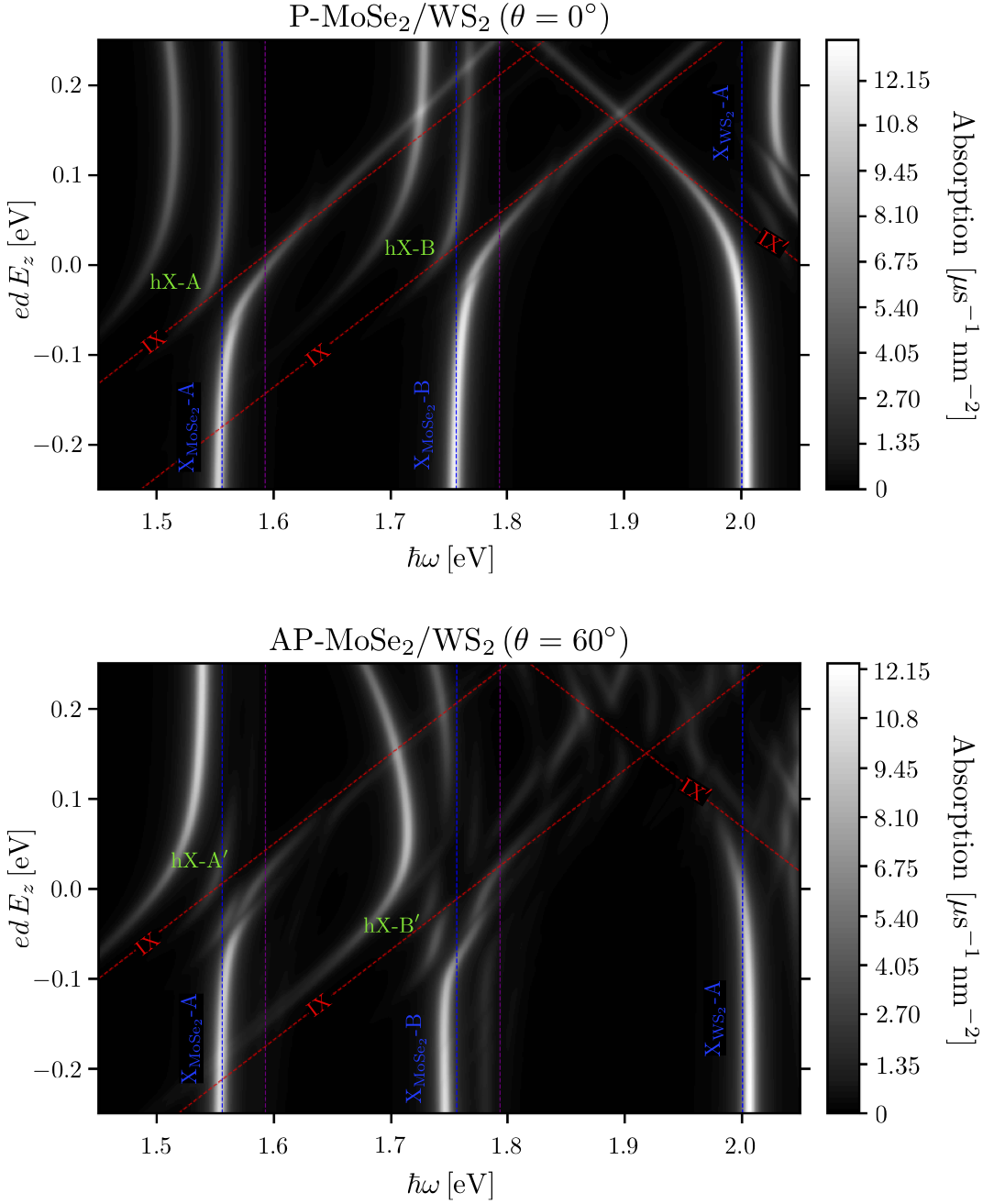
VI.3 hX fine structure due to mSL-induced umklapp electron-photon interaction
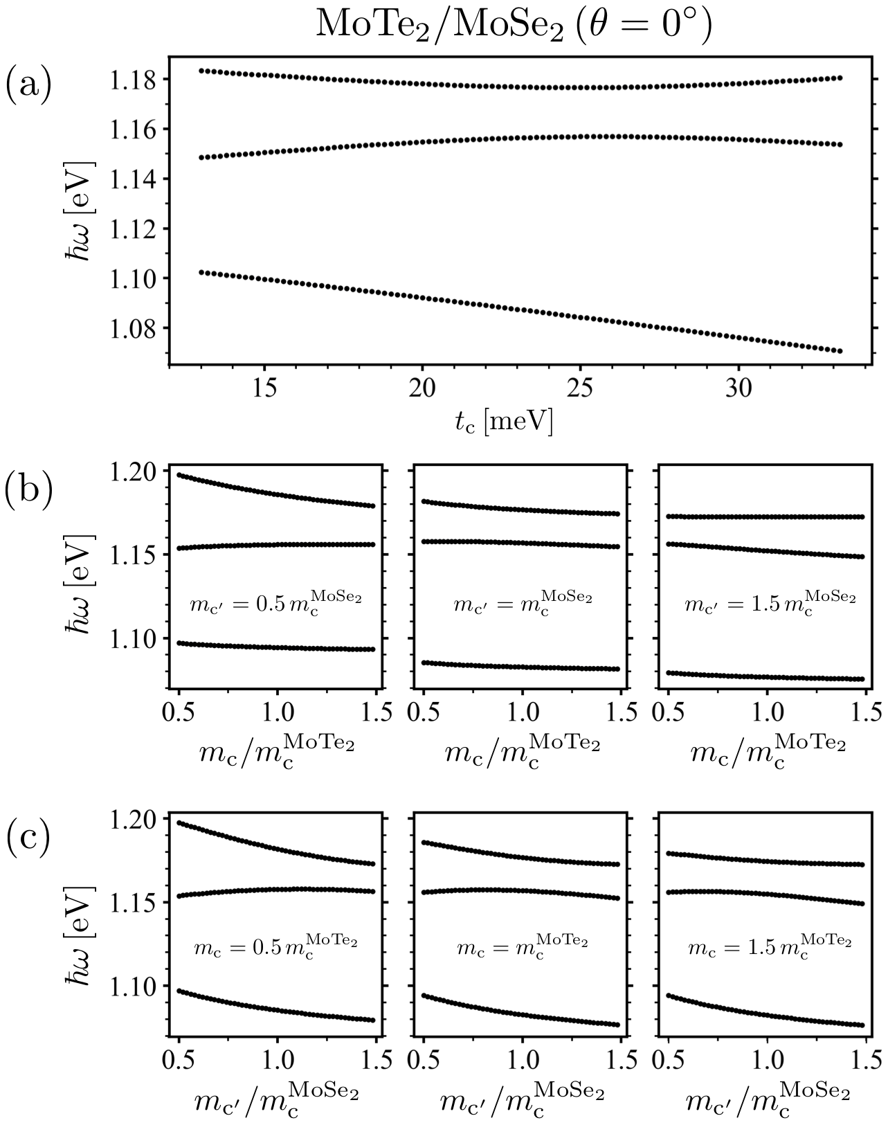
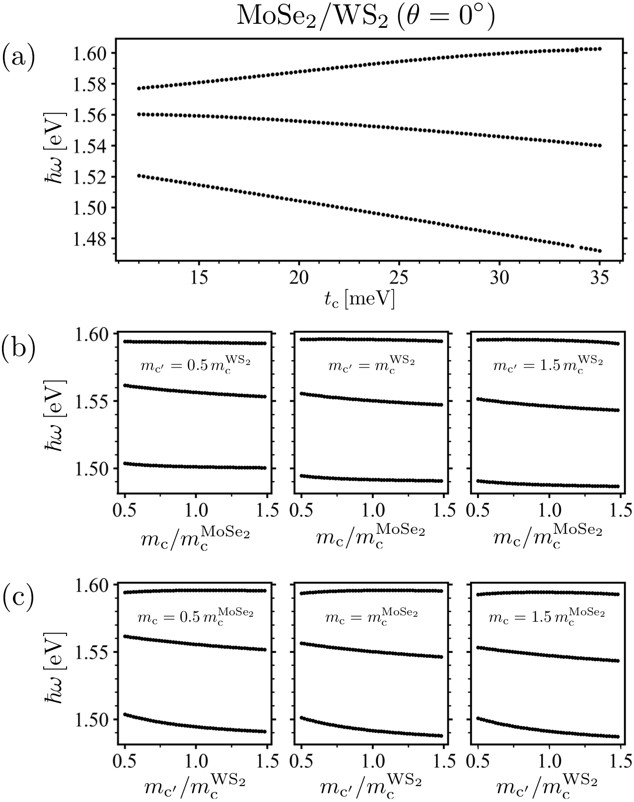
Perhaps, the most important features appearing in Fig. 19 are the additional absorption lines indicated by white arrows, which accompany the hX-A and hX-B signatures for or , especially pronounced for MoSe2/WS2. These lines originate from the minibands obtained by the first folding of the A or B intralayer exciton dispersion into the mBZ, to the new point. These states become optically active due to umklapp photon absorption processes, in which a mSL Bragg vector is transferred to the crystal, thus making exciton states with finite momenta , and bright. This is depicted in the right panels of Fig. 19. The presence of these lines can provide direct evidence of moiré superlattice effects. We have verified that, for aligned MoTe2/MoSe2 and MoSe2/WS2 heterostructures, the three-peak spectra produced by the two main hX lines and the third umklapp line are robust to variation of the main theoretical parameters considered (the interlayer electron hopping energy , and the conduction-band masses of the two TMD layers), and should thus be visible in real samples with different preparation methods, and under different conditions. This is shown in Figures 24 and 25 of Appendix C.
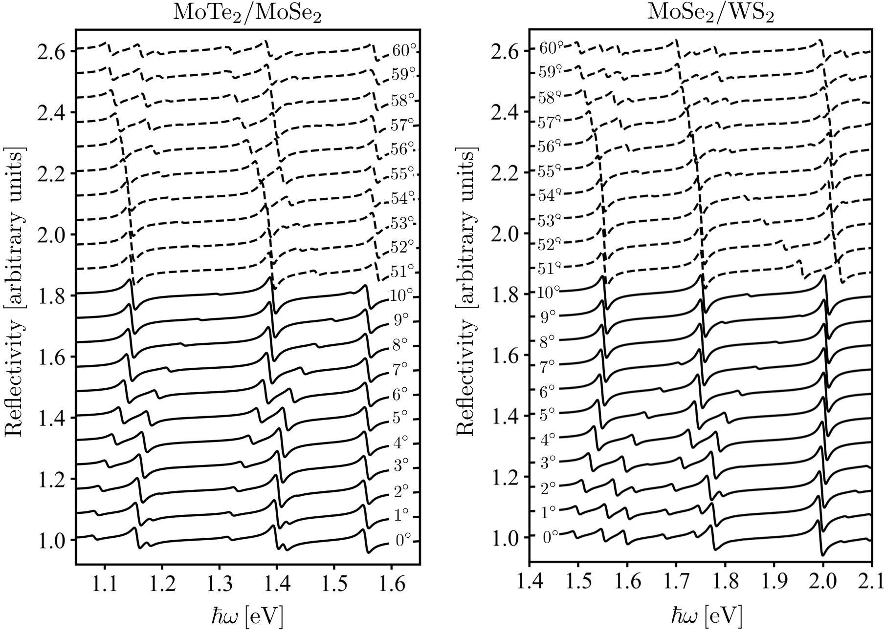
Figs. 21 and 22 show that the umklapp photon absorption lines disappear below some negative electric field value, but remain bright for , and can be identified with the purple reference lines corresponding to the energy of the first folded A or B -exciton, up to an overall red shift due to interaction with higher-energy IX minibands. The splitting of this triad formed by the two hX-A or -B lines and the first A or B umklapp photon absorption line, into a pair of lines that do not undergo a Stark shift, plus one that does, can serve to identify both the hybridized exciton physics and the moiré superlattice effects in an experimental setting. As a final remark, we note that the optical spectra of TMD heterostructures are normally measured through their reflectivity, rather than absorption properties. Figure 23 shows our prediction for the reflectivity spectra of MoTe2/MoSe2 and MoSe2/WS2, obtained from our absorption calculations via a Kramers-Kronig relation Landau et al. (2013).
VII Conclusions
We have studied the interplay between band alignment and the presence of emergent moiré superlattices (mSL) in twisted heterobilayers of transition-metal dichalcogenides (TMDs). Starting from a microscopic interlayer tunneling Hamiltonian, we have derived effective harmonic-potentials based on perturbation theory, to describe the effects of moiré patterns on the electron and hole bands of TMD heterostructures with large interlayer offsets between carrier band edges. We have shown that this approach fails in TMD homobilayers, and in heterostructures such as MoSe2/WS2 and MoTe2/MoSe2, where bands of the two constituent monolayers hybridize resonantly. Our results show that the influence of higher moiré superlattice minibands for the low-energy electron band structure in these heterobilayers becomes increasingly important as the interlayer band-edges offset is reduced; in other words, that resonant interlayer hybridization amplifies the moiré superlattice effects on the electronic structure. By treating hybridization effects exactly, we have predicted the appearance of van Hove singularities near the conduction miniband edges in these materials close to perfect alignment, of potential interest for the study of strongly correlated electron physics in TMDs.
We have also developed a general description of low-energy excitons in TMD heterobilayers, and found that the small interlayer conduction-band-edge detunings in MoSe2/WS2 and MoTe2/MoSe2 result in nearly degenerate intralayer and interlayer exciton states, with the resonant condition further enhanced by the difference in binding energies of these two exciton species. This gives rise to hybridized excitons (hXs), which inherit the brightness of intralayer excitons and the polar nature of interlayer excitons. Presently, our model neglects the effects of periodic strain that may develop in each layer of the heterostructure, and which can affect the energies of the band edges. Such effects may be most important for the best lattice-matched and highly aligned structures (e.g., WSe2/MoSe2 and WSe2/WS2), as well as homobilayers, and should be added on top of the hybridization effects studied here. Using experimental values for the exciton energies reported in the literature on TMD heterobilayers, we have evaluated the full optical spectra of MoSe2/WS2 and MoTe2/MoSe2 heterostructures, and made predictions for explicit signatures of strong intralayer-interlayer exciton hybridization, and of the presence of the moiré superlattice. Hence, we predict that mSL-modified hXs should be ubiquitous to TMD heterostructures, and dominate the low-energy spectrum of closely aligned TMD heterobilayers with near resonant band edges, in agreement with recent experimental developments Alexeev et al. (2019).
Acknowledgements.
The authors acknowledge funding by the EU Graphene Flagship Project, ERC Synergy Grant Hetero2D, EPSRC Grand Challenges Grant, Lloyd Register Foundation Nanotechnology Grant, European Quantum Technologies Flagship Project, and EPSRC grant EP/P026850/1. We would like to thank E.M. Alexeev, M. Danovich, F.H.L. Koppens, A. Kozikov, K.S. Novoselov, M. Potemski, A.I. Tartakovskii, J.R. Wallbank and V. Zólyomi for fruitful discussions at various stages of this work.References
- Geim and Grigorieva (2013) A. K. Geim and I. V. Grigorieva, Nature 499, 419 (2013).
- Novoselov et al. (2016) K. S. Novoselov, A. Mishchenko, A. Carvalho, and A. H. Castro Neto, Science 353 (2016), 10.1126/science.aac9439.
- Ponomarenko et al. (2013) L. A. Ponomarenko, R. V. Gorbachev, G. L. Yu, D. C. Elias, R. Jalil, A. A. Patel, A. Mishchenko, A. S. Mayorov, C. R. Woods, J. R. Wallbank, M. Mucha-Kruczynski, B. A. Piot, M. Potemski, I. V. Grigorieva, K. S. Novoselov, F. Guinea, V. I. Fal’ko, and A. K. Geim, Nature 497, 594 (2013).
- Dean et al. (2013) C. R. Dean, L. Wang, P. Maher, C. Forsythe, F. Ghahari, Y. Gao, J. Katoch, M. Ishigami, P. Moon, M. Koshino, T. Taniguchi, K. Watanabe, K. L. Shepard, J. Hone, and P. Kim, Nature 497, 598 (2013).
- Hunt et al. (2013) B. Hunt, J. D. Sanchez-Yamagishi, A. F. Young, M. Yankowitz, B. J. LeRoy, K. Watanabe, T. Taniguchi, P. Moon, M. Koshino, P. Jarillo-Herrero, and R. C. Ashoori, Science 340, 1427 (2013).
- Li et al. (2010) G. Li, A. Luican, J. M. B. Lopes Dos Santos, A. H. Castro Neto, A. Reina, J. Kong, and E. Y. Andrei, Nat. Phys. 6, 109 (2010).
- Yankowitz et al. (2012) M. Yankowitz, J. Xue, D. Cormode, J. D. Sanchez-Yamagishi, K. Watanabe, T. Taniguchi, P. Jarillo-Herrero, P. Jacquod, and B. J. LeRoy, Nat. Phys. 8, 382 (2012).
- Krishna Kumar et al. (2018) R. Krishna Kumar, A. Mishchenko, X. Chen, S. Pezzini, G. H. Auton, L. A. Ponomarenko, U. Zeitler, L. Eaves, V. I. Fal’ko, and A. K. Geim, PNAS 115, 5135 (2018).
- Yu et al. (2014) G. L. Yu, R. V. Gorbachev, J. S. Tu, A. V. Kretinin, Y. Cao, R. Jalil, F. Withers, L. A. Ponomarenko, B. A. Piot, M. Potemski, D. C. Elias, X. Chen, K. Watanabe, T. Taniguchi, I. V. Grigorieva, K. S. Novoselov, V. I. Fal’ko, A. K. Geim, and A. Mishchenko, Nat. Phys. 10, 525 (2014).
- Ni et al. (2015) G. X. Ni, H. Wang, J. S. Wu, Z. Fei, M. D. Goldflam, F. Keilmann, B. Özyilmaz, A. H. Castro Neto, X. M. Xie, M. M. Fogler, and D. N. Basov, Nat. Mat. 14, 1217 (2015).
- Hsu et al. (2014) W.-T. Hsu, Z.-A. Zhao, L.-J. Li, C.-H. Chen, M.-H. Chiu, P.-S. Chang, Y.-C. Chou, and W.-H. Chang, ACS Nano 8, 2951 (2014).
- Rigosi et al. (2015) A. F. Rigosi, H. M. Hill, Y. Li, A. Chernikov, and T. F. Heinz, Nano Lett. 15, 5033 (2015).
- Hill et al. (2016) H. M. Hill, A. F. Rigosi, K. T. Rim, G. W. Flynn, and T. F. Heinz, Nano Lett. 16, 4831 (2016).
- Nayak et al. (2017) P. K. Nayak, Y. Horbatenko, S. Ahn, G. Kim, J.-U. Lee, K. Y. Ma, A.-R. Jang, H. Lim, D. Kim, S. Ryu, H. Cheong, N. Park, and H. S. Shin, ACS Nano 11, 4041 (2017).
- Alexeev et al. (2017) E. M. Alexeev, A. Catanzaro, O. V. Skrypka, P. K. Nayak, S. Ahn, S. Pak, J. Lee, J. I. Sohn, K. S. Novoselov, H. S. Shin, and A. I. Tartakovskii, Nano Lett. 17, 5342 (2017).
- Zhang et al. (2017) C. Zhang, C.-P. Chuu, X. Ren, M.-Y. Li, L.-J. Li, C. Jin, M.-Y. Chou, and C.-K. Shih, Sci. Adv. 3 (2017), 10.1126/sciadv.1601459.
- Mak et al. (2010) K. F. Mak, C. Lee, J. Hone, J. Shan, and T. F. Heinz, Phys. Rev. Lett. 105, 136805 (2010).
- Splendiani et al. (2010) A. Splendiani, L. Sun, Y. Zhang, T. Li, J. Kim, C.-Y. Chim, G. Galli, and F. Wang, Nano Lett. 10, 1271 (2010).
- Wang et al. (2018) G. Wang, A. Chernikov, M. M. Glazov, T. F. Heinz, X. Marie, T. Amand, and B. Urbaszek, Rev. Mod. Phys. 90, 021001 (2018).
- Yao et al. (2008) W. Yao, D. Xiao, and Q. Niu, Phys. Rev. B 77, 235406 (2008).
- Zeng et al. (2012) H. Zeng, J. Dai, W. Yao, D. Xiao, and X. Cui, Nat. Nanotechnol. 7, 490 (2012).
- Mak et al. (2012) K. F. Mak, K. He, J. Shan, and T. F. Heinz, Nat. Nanotechnol. 7, 494 (2012).
- Kuwabara et al. (1990) M. Kuwabara, D. R. Clarke, and D. A. Smith, Applied Physics Letters 56, 2396 (1990).
- Wu et al. (2018a) F. Wu, T. Lovorn, E. Tutuc, and A. H. MacDonald, Phys. Rev. Lett. 121, 026402 (2018a).
- Cao et al. (2018) Y. Cao, V. Fatemi, S. Fang, K. Watanabe, T. Taniguchi, E. Kaxiras, and P. Jarillo-Herrero, Nature 556, 43 (2018).
- Gong et al. (2013) C. Gong, H. Zhang, W. Wang, L. Colombo, R. M. Wallace, and K. Cho, Appl. Phys. Lett. 103, 053513 (2013).
- Xu et al. (2018) K. Xu, Y. Xu, H. Zhang, B. Peng, H. Shao, G. Ni, J. Li, M. Yao, H. Lu, H. Zhu, and C. M. Soukoulis, Phys. Chem. Chem. Phys. 20, 30351 (2018).
- Kozawa et al. (2016) D. Kozawa, A. Carvalho, I. Verzhbitskiy, F. Giustiniano, Y. Miyauchi, S. Mouri, A. H. C. Neto, K. Matsuda, and G. Eda, Nano Lett. 16, 4087 (2016).
- Bistritzer and MacDonald (2011) R. Bistritzer and A. H. MacDonald, PNAS 108, 12233 (2011).
- Wu et al. (2017) F. Wu, T. Lovorn, and A. H. MacDonald, Phys. Rev. Lett. 118, 147401 (2017).
- Yu et al. (2017) H. Yu, G.-B. Liu, J. Tang, X. Xu, and W. Yao, Sci. Adv. 3, e1701696 (2017).
- Wu et al. (2018b) F. Wu, T. Lovorn, and A. H. MacDonald, Phys. Rev. B 97, 035306 (2018b).
- Tong et al. (2016) Q. Tong, H. Yu, Q. Zhu, Y. Wang, X. Xu, and W. Yao, Nat. Phys. 13, 356 (2016).
- Note (1) An alternative nomenclature is used, e.g., in Refs. \rev@citealpnumwang_yao_tvvtcc,wangyao_coupling, where P and AP stacking configurations are referred to as R and H stacking, respectively. We choose the former convention to avoid confusion with standard nomenclature for commensurate stacking.
- Constantinescu et al. (2013) G. Constantinescu, A. Kuc, and T. Heine, Phys. Rev. Lett. 111, 036104 (2013).
- He et al. (2014) J. He, K. Hummer, and C. Franchini, Phys. Rev. B 89, 075409 (2014).
- Kormányos et al. (2015) A. Kormányos, G. Burkard, M. Gmitra, J. Fabian, V. Zólyomi, N. D. Drummond, and V. Fal’ko, 2D Materials 2, 022001 (2015).
- Kylänpää and Komsa (2015) I. Kylänpää and H.-P. Komsa, Phys. Rev. B 92, 205418 (2015).
- Cheiwchanchamnangij and Lambrecht (2012) T. Cheiwchanchamnangij and W. R. L. Lambrecht, Phys. Rev. B 85, 205302 (2012).
- Wang et al. (2017a) Y. Wang, Z. Wang, W. Yao, G.-B. Liu, and H. Yu, Phys. Rev. B 95, 115429 (2017a).
- Kormányos et al. (2018) A. Kormányos, V. Zólyomi, V. I. Fal’ko, and G. Burkard, Phys. Rev. B 98, 035408 (2018).
- Alexeev et al. (2019) E. M. Alexeev, D. A. Ruiz-Tijerina, M. Danovich, M. J. Hamer, D. J. Terry, P. K. Nayak, S. Ahn, S. Pak, J. Lee, J. I. Sohn, M. R. Molas, M. Koperski, K. Watanabe, T. Taniguchi, K. S. Novoselov, R. V. Gorbachev, H. S. Shin, V. I. Fal’ko, and A. I. Tartakovskii, Nature 567, 81 (2019).
- Mostaani et al. (2017) E. Mostaani, M. Szyniszewski, C. H. Price, R. Maezono, M. Danovich, R. J. Hunt, N. D. Drummond, and V. I. Fal’ko, Phys. Rev. B 96, 075431 (2017).
- Al-Hilli and Evans (1972) A. A. Al-Hilli and B. L. Evans, Journal of Crystal Growth 15, 93 (1972).
- Kindermann et al. (2012) M. Kindermann, B. Uchoa, and D. L. Miller, Phys. Rev. B 86, 115415 (2012).
- Wallbank et al. (2013) J. R. Wallbank, A. A. Patel, M. Mucha-Kruczyński, A. K. Geim, and V. I. Fal’ko, Phys. Rev. B 87, 245408 (2013).
- Schrieffer and Wolff (1966) J. R. Schrieffer and P. A. Wolff, Phys. Rev. 149, 491 (1966).
- Wallbank et al. (2015) J. R. Wallbank, M. Mucha-Kruczyński, X. Chen, and V. I. Fal’ko, Annalen der Physik 527, 359 (2015).
- Koshino and Moon (2015) M. Koshino and P. Moon, Journal of the Physical Society of Japan 84, 121001 (2015).
- Xiao et al. (2012) D. Xiao, G.-B. Liu, W. Feng, X. Xu, and W. Yao, Phys. Rev. Lett. 108, 196802 (2012).
- Rivera et al. (2015) P. Rivera, J. R. Schaibley, A. M. Jones, J. S. Ross, S. Wu, G. Aivazian, P. Klement, K. Seyler, G. Clark, N. J. Ghimire, J. Yan, D. G. Mandrus, W. Yao, and X. Xu, Nat. Commun. 6, 6242 (2015).
- Klein et al. (2016) J. Klein, J. Wierzbowski, A. Regler, J. Becker, F. Heimbach, K. Müller, M. Kaniber, and J. J. Finley, Nano Lett. 16, 1554 (2016).
- Wang et al. (2017b) K.-C. Wang, T. K. Stanev, D. Valencia, J. Charles, A. Henning, V. K. Sangwan, A. Lahiri, D. Mejia, P. Sarangapani, M. Povolotskyi, A. Afzalian, J. Maassen, G. Klimeck, M. C. Hersam, L. J. Lauhon, N. P. Stern, and T. Kubis, Journal of Applied Physics 122, 224302 (2017b).
- Berkelbach et al. (2013) T. C. Berkelbach, M. S. Hybertsen, and D. R. Reichman, Phys. Rev. B 88, 045318 (2013).
- Kumar and Ahluwalia (2012) A. Kumar and P. Ahluwalia, Physica B: Condens. Matter 407, 4627 (2012).
- Danovich et al. (2018) M. Danovich, D. A. Ruiz-Tijerina, R. J. Hunt, M. Szyniszewski, N. D. Drummond, and V. I. Fal’ko, Phys. Rev. B 97, 195452 (2018).
- Heo et al. (2015) H. Heo, J. H. Sung, S. Cha, B.-G. Jang, J.-Y. Kim, G. Jin, D. Lee, J.-H. Ahn, M.-J. Lee, J. H. Shim, H. Choi, and M.-H. Jo, Nat. Commun. 6, 7372 (2015).
- Zhu et al. (2017) H. Zhu, J. Wang, Z. Gong, Y. D. Kim, J. Hone, and X.-Y. Zhu, Nano Lett. 17, 3591 (2017).
- Deilmann and Thygesen (2018) T. Deilmann and K. S. Thygesen, Nano Lett. 18, 2984 (2018).
- Keldysh (1979) L. V. Keldysh, Pis’ma Zh. Eksp. Teor. Phys. 29, 716 (1979), [JETP Lett. 29, 659 (1979)].
- Moskalenko and Snoke (2000) S. A. Moskalenko and D. W. Snoke, Bose-Einstein condensation of excitons and biexcitons and coherent nonlinear optics with excitons (Cambridge University Press, 2000).
- Yu et al. (2015) H. Yu, Y. Wang, Q. Tong, X. Xu, and W. Yao, Phys. Rev. Lett. 115, 187002 (2015).
- Gong et al. (2014) Y. Gong, J. Lin, X. Wang, G. Shi, S. Lei, Z. Lin, X. Zou, G. Ye, R. Vajtai, B. I. Yakobson, H. Terrones, M. Terrones, B. K. Tay, J. Lou, S. T. Pantelides, Z. Liu, W. Zhou, and P. M. Ajayan, Nat. Mater. 13, 1135 (2014).
- Nagler et al. (2017) P. Nagler, G. Plechinger, M. V. Ballottin, A. Mitioglu, S. Meier, N. Paradiso, C. Strunk, A. Chernikov, P. C. M. Christianen, C. Schüller, and T. Korn, 2D Mat. 4, 025112 (2017).
- Zhang et al. (2018) N. Zhang, A. Surrente, M. Baranowski, D. K. Maude, P. Gant, A. Castellanos-Gomez, and P. Plochocka, Nano Lett. 18, 7651 (2018), https://doi.org/10.1021/acs.nanolett.8b03266 .
- Kozawa et al. (2014) D. Kozawa, R. Kumar, A. Carvalho, K. Kumar Amara, W. Zhao, S. Wang, M. Toh, R. M. Ribeiro, A. H. Castro Neto, K. Matsuda, and G. Eda, Nat. Commun. 5, 4543 (2014).
- Ruppert et al. (2014) C. Ruppert, O. B. Aslan, and T. F. Heinz, Nano Lett. 14, 6231 (2014).
- Lezama et al. (2015) I. G. Lezama, A. Arora, A. Ubaldini, C. Barreteau, E. Giannini, M. Potemski, and A. F. Morpurgo, Nano Lett. 15, 2336 (2015).
- Robert et al. (2016) C. Robert, R. Picard, D. Lagarde, G. Wang, J. P. Echeverry, F. Cadiz, P. Renucci, A. Högele, T. Amand, X. Marie, I. C. Gerber, and B. Urbaszek, Phys. Rev. B 94, 155425 (2016).
- Zhao et al. (2013) W. Zhao, Z. Ghorannevis, L. Chu, M. Toh, C. Kloc, P.-H. Tan, and G. Eda, ACS Nano 7, 791 (2013).
- Landau et al. (2013) L. D. Landau, E. M. Lifshitz, and L. P. Pitaevskii, Electrodynamics of continuous media, 2nd ed. (Elsevier, 2013).
Appendix A Photoluminescence of hybridized excitons
To estimate the photoluminescence (PL) intensity of a TMD heterobilayer , we assume a photoexcited thermal population of excitons described by the Bose-Einstein distribution
| (36) |
where is the global minimum of the exciton moiré band structure.
The light-matter interaction Hamiltonian is given by
| (37) |
where the operator creates a photon of momentum and circular polarization ( corresponding to counter-clockwise and clockwise polarization, respectively); and are the momentum matrix elements at the - and -layer valleys, respectively (Table 3); and , with the heterostructure surface area, and the height of the optical cavity. We evaluate the radiative decay (number of photons per unit time) of hXs perturbatively, using Fermi’s golden rule in its thermodynamic form
| (38) |
with single-photon final states , and initial states
| (39) |
The indices number the minibands, and stand for the double index introduced in Eq. (19), and . With the definitions of Eq. (30), we obtain the matrix elements
| (40) |
Note that for (P stacking), Fermi’s golden rule will give interference between the last two terms in Eq. (40), whereas no interference occurs for (AP stacking). Keeping this in mind, we will focus on the latter case, for the sake of concreteness. Fermi’s golden rule gives
| (41) |
Given the steepness of the photon dispersion relation, all terms with are removed by the Dirac delta function in (41). Moreover, only light-cone excitons with center-of-mass momentum can recombine, according to energy-momentum conservation. Given the smallness of , we set for the exciton dispersions and wave-function coefficients in (41). After taking the continuum limit for to evaluate the sum as an integral, we find that
| (42) |
The total PL intensity (photons per unit time per unit area) is obtained by evaluating this integral, and further integrating the resulting expression over exciton wave number within the light cone, finally giving
| (43) |
A significant exciton population will only exist in the few lowest-energy minibands, so we evaluate only and . The main PL line appears for photon energies , and has an activation temperature given by [Figs. 18(c) and 18(d)]. For Fig. 19, we have introduced a Lorentzian line shape
with phenomenological broadening .
Appendix B Optical absorption by hybridized excitons
For the heterostructure’s optical absorption spectrum (number of photons absorbed per unit time per unit area), we have used the version of Fermi’s golden rule, with relaxed energy conservation (line broadening):
| (44) |
setting , and [see Eq. (39)]. After some algebra, we obtain the absorption rate for photons of momentum and polarization given by
| (45) |
The total number of absorbed photons is obtained by multiplying this expression by the number of photons states in the infinitesimal energy range to ; that is, the number of photons with wave number of magnitude between and . Since the reciprocal volume elements is , and each volume element contains photon states, this number of photons is . The resulting total absorption rate from exciton band is given by
| (46) |
In an experimental setup, the energy differential can be identified with the detector’s resolution, which we set to , together with the phenomenological line broadening , to produce the spectra of Figs. 2, 19–22.
Appendix C Dependence of the MoTe2/MoSe2 and MoSe2/WS2 optical spectra on the model parameters
We evaluated the low-energy absorption spectra of perfectly aligned () MoTe2/MoSe2 and MoSe2/WS2, for different values of the relevant parameters in our theoretical model: the interlayer electron tunneling energy and the conduction- and valence-band masses and . The latter two parameters affect the intra- and interlayer exciton masses and Bohr radii, such that the intralayer-interlayer exciton mixing energies of Eq. (35) are modified by all three parameters. Therefore, for each combination of and , we evaluated the relevant exciton Bohr radii using the finite elements method discussed in Sec. VI. Figs. 24 and 25 show the variation of the three main hX absorption peaks discussed in the main text with varying , and within of their reference values. The weak dependence found for both material pairs indicates that the three-peak structure should appear for samples of different qualities, and prepared by different methods, where all three parameters may vary.