Suspended silicon nitride thin films with enhanced and electrically tunable reflectivity
Abstract
We report on the realization of silicon nitride membranes with enhanced and electrically tunable reflectivity. A subwavelength one-dimensional grating is directly patterned on a suspended 200 nm-thick, high stress commercial film using electron beam lithography. A Fano resonance is observed in the transmission spectrum of TM polarized light impinging on the membrane at normal incidence, leading to an increase in its reflectivity from 10% to 78% at 937 nm. The observed spectrum is compared to the results of rigorous coupled wave analysis simulations based on measurements of the grating transverse profile through localized cuts of the suspended film with a Focused Ion Beam. By mounting the membrane chip on a ring piezoelectric transducer and applying a compressive force to the substrate we subsequently observe a shift of the transmission spectrum by 0.23 nm.
1 Introduction
Suspended thin films are widely used in photonics and sensing applications. Among them, silicon nitride films deposited with low pressure chemical vapor deposition benefit from excellent optical properties, high refractive index and ultralow loss in the visible and near-infrared range, as well outstanding mechanical properties, high frequency/quality factor mechanical resonances and high burst pressure. Due to these features as well as their low mass, thin SiN films with thickness ranging from tens to a few hundreds of nanometers have been applied in a number of cavity optomechanics investigations [1, 2, 3, 4, 5, 6, 7, 8, 9]. Increasing the otherwise relatively low reflectivity of such membranes without increasing their mass is beneficial for cavity optomechanics with single [10, 11, 12, 13, 14, 15, 16, 17, 18] or multiple resonators [19, 20, 21, 22, 23, 24, 25], as well as for sensing [26, 27, 28] or lasing [29, 30, 31] applications. Such an increase in reflectivity for films with subwavelength thickness can be realized by patterning the film with a suitable subwavelength periodic structure, such as a high contrast grating [32] or a photonic crystal structure [33]. The interference between the incoming light and guided modes in the structure allows for tailoring the optical properties of the film. In particular, the destructive interference occuring for specific wavelengths/polarizations can give rise to the appearance of either broad- or narrowband Fano-like resonances in the reflectivity spectrum [34]. In a broader context, resonant waveguide gratings and photonic crystal structures are relevant for a variety of optical applications, including waveguide coupling, optical filtering, polarizers, spectrometry, biosensing, solar cells, photodetection, lasing, etc. [35].
Enhanced reflectivity of suspended silicon nitride membranes has been observed both for two-dimensional photonic crystals [12, 14, 15, 17, 18, 36] and for one-dimensional subwavelength gratings (SG) [10, 11, 13] patterning. We focus here on the realization of polarization-dependent, one-dimensional SGs similar to those of Refs. [10, 11, 37, 13], albeit by following the approach of [17] and directly patterning a m2 subwavelength grating on a commercial, 200 nm-thick silicon nitride membrane. A Fano resonance is observed in the transmission spectrum of transverse magnetic (TM) polarized light impinging at normal incidence, showing an increase in reflectivity at 937 nm from 10% for an unpatterned membrane to 78% for a patterned one. By using localized cuts of the structure with a Focused Ion Beam [38] we also show that the grating transverse grating profile of the suspended film can be measured. We compare the observed transmission spectrum with the results of Rigorous Coupled Wave Analysis numerical simulations taking into account the grating profile and discuss collimation broadening and finite grating size effects.
Last, by mounting the membrane chip on a ring piezoelectric transducer and applying a compressive force to the corners of the substrate we show as a proof of principle that it is possible to shift the transmission spectrum by 0.23 nm towards lower wavelengths. Optimizing and increasing the piezoelectric compressive force further would make such patterned membranes interesting for realizing tunable optical filters [37], waveplates [39] or strongly focusing lenses [40, 41, 42]. Increasing the patterned area [17, 18] and the reflectivity would also make them attractive for vertical-cavity surface-emitting lasers [29, 43] or optical sensors [27, 28] for biophysics [44, 45] and biomedical [46, 47] applications. Last, combined with piezoelectric actuation of their mechanical modes [48, 49], such enhanced and electrically tunable reflectivity membranes would be particularly interesting for improving and tailoring the optomechanical response of arrays of nanomembranes [50, 25, 36] and for investigating collective and strong coupling optomechanics [21, 51, 22, 52, 53].
2 Fabrication
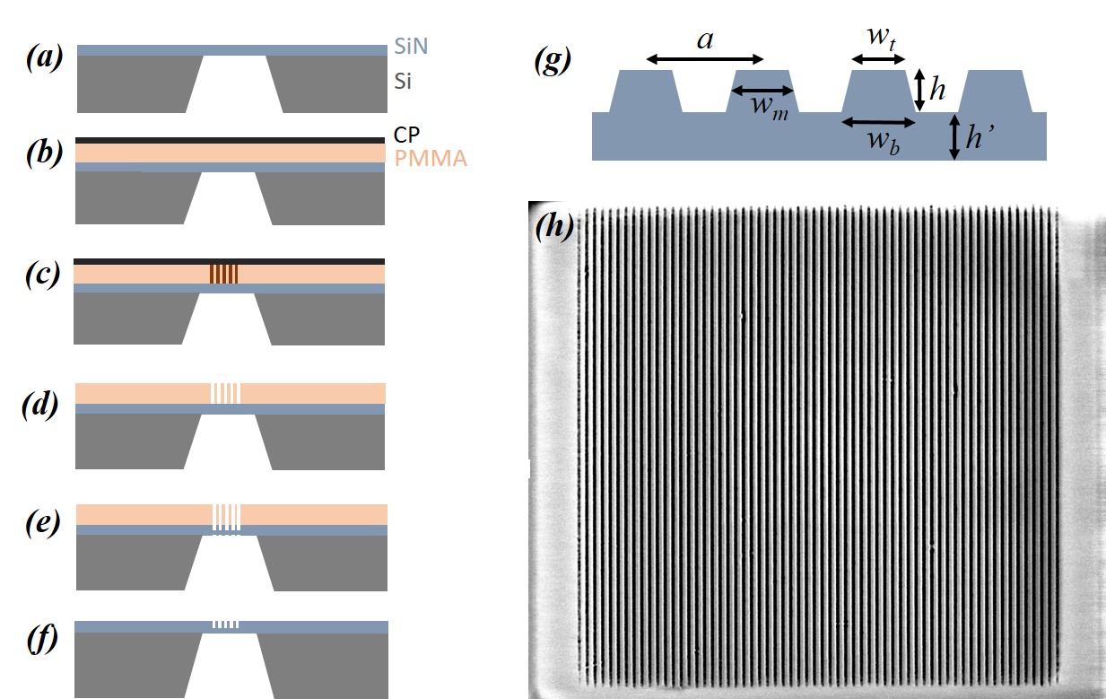
The stochiometric silicon nitride membranes used in this work are commercial [54], high stress (GPa), 0.5 mm-square and 200 nm-thick films on a 5 mm-square, 500 m-thick silicon frame. The steps for patterning the SG are depicted in Fig. 1a and are as follows: after cleaning with an O2 plasma the sample is spin-coated with a 9% 950k molecular weight PMMA resist and a conductive polymer layer (SX-AR-PC 5000/90.2) to avoid charging effects during Electron Beam Lithography (EBL). A m2 grating mask with a target period and finger width is then written by EBL at 30 kV. After writing the conductive polymer layer is removed by immersion in deionized water and the PMMA resist is developed in a solution of 3:7 H2O:IPA (Iso-propyl alcohol). The membrane is then etched in a STS Pegasus ICP DRIE system using reactive ion etching with C4F8 (flow rate 59 sccm) and SF6 (flow rate 36 sccm) for 170 seconds at 800 W. The PMMA layer is removed in acetone followed by rinsing in IPA and N2 blow drying. The sample is finally cleaned by means of the O2 plasma again.
The etching parameters are observed to be quite critical for the success of the patterning, and etching only a fraction of the 200 nm films is determinant in avoiding rupture/damage during the process. A top-view SEM picture of the resulting grating is shown in Fig. 1h. From such SEM images the period and grating finger width are estimated to be nm and nm, respectively, where the uncertainties come from the imaging system calibration. The latter number is potentially deceiving, however, as the vertical profile of the grating is not expected to be rectangular and the observed mean finger width depends on the saturation level of the SEM image.
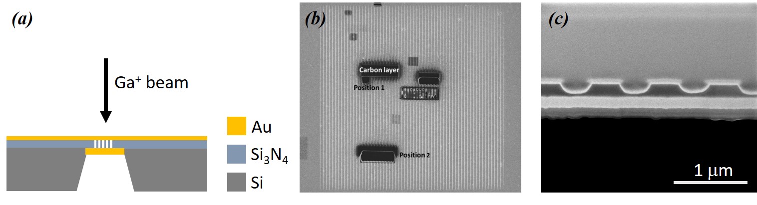
To get more insight into the vertical profile of the grating structure a Focused Ion Beam (FIB) was used to cut through the SG at different locations of the patterned area, as shown in Figs. 2a and b. Before the FIB cut the membrane was made more robust by coating on both the etched and non etched sides with nm and nm of gold, respectively, and a thick (m) carbon layer was deposited at the various cutting positions. The gold layers prevent the structure from fracturing and breaking when exposed to the ion beam. Cuts in several locations of the same grating can then be performed, as illustrated in Fig. 2b. A high energy Ga+ ion beam is focused at the edge of the cutting positions defined by the carbon layers, as shown in Figs. 2a and b. The grating cross section can then be imaged at a 45∘ angle with a SEM microscope (Fig. 2c). As expected, the grating fingers are observed to have smooth edged walls, whose width substantially varies from top to bottom. Analyzing these images yield for this particular sample a period nm, mean/top/bottom/mean finger widths of nm, nm and nm, respectively. The grating height is nm and the underlying Si3N4 layer thickness nm. The transverse profile obtained from these images can be used as input to the numerical simulations to predict transmission spectra, as will be discussed below.
3 Optical characterization
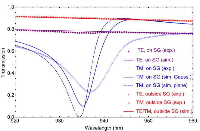
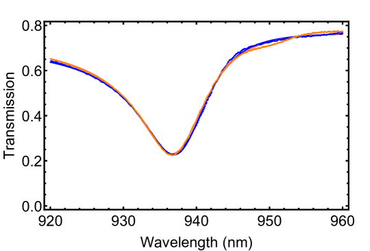
The transmission of a patterned membrane similar to the one described in the previous section was measured by focusing onto the sample linearly polarized light issued from a tunable external cavity diode laser with a mm focal length achromat doublet (spotsize 30 m). Figure 3 shows the normalized transmission measured for TE and TM polarized light impinging at normal incidence either on or outside the patterned area.
Outside the patterned area the transmissivity of the film is independent of the polarization of the light and its level is determined by the film thickness and refractive index. From ellipsometry measurements and broadband transmission spectroscopy [50] the thickness and refractive index of unprocessed samples from the same fabrication batch were determined to be nm and in the plotted range (920-960 nm). Consistently with these values the measured transmissiondecreases from 12 to 8% in that range. When light impinges on the patterned area an overall small drop in transmission is observed for TE polarized light, on account of the reduced effective thickness of the patterned film. A much more stronger wavelength-dependent drop is observed for TM polarized light around 937 nm, as a result of the interference between the incoming light and guided modes in the structure in this wavelength range.
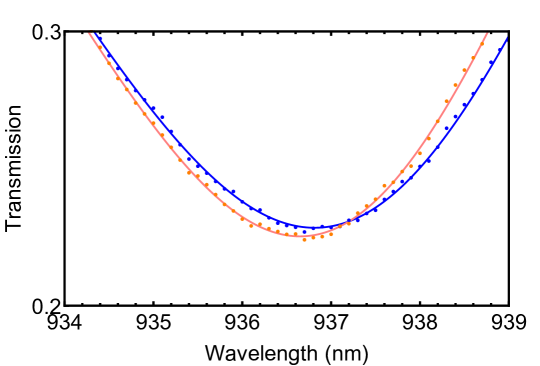
To investigate the observed spectrum we performed numerical simulations based on a RCWA approach [55] and using as input parameters the refractive index determined previously, the grating period nm and mean finger width nm estimated from topview SEM images and the approximate grating profile shown in Fig. 1g with the thicknesses nm and nm determined from the FIB cut measurements. In this approach a plane wave is incident on an infinite grating, whose unit cell is defined by the previous parameters (20 layers were used to discretize the structure), and the transmitted or reflected fields can be computed. The dashed blue line in Fig. 3 shows the result of such a simulation for a plane wave impinging on the grating at normal incidence (), which predicts a narrower Fano resonance with zero transmission occuring around 934.5 nm. The beam incident on the grating is however a focused Gaussian beam with a waist m. This beam can be considered as a superposition of plane waves impinging on the grating with various incident angles [56, 14, 18]. The transmittivity of the collimated beam is then computed by performing a weighted average of the RCWA-simulated transmittivities of plane waves incident at different angles, with a Gaussian distribution , where is the Gaussian beam divergence angle ( in our case). The resulting spectrum (solid blue line in Fig. 3) shows a shifted and broadened Fano resonance displaying non-zero minimal transmission, as compared to the infinite plane wave case, and is closer to the measured spectrum, although the latter is somehow still more shifted and broadened. Slightly altering the grating parameters in the simulations around the measured values within the systematic uncertainties does not qualitatively change this picture; while collimation broadening can be expected to play a non-negligible role, other effects are likely to contribute to the broadening and shifting of the spectrum. Effects due to the finite size of the grating could also play a role. These could in principle be numerically simulated using full three-dimensional finite element analysis; however, such simulations are computationally heavy and were not performed here. Instead, we note that an estimate of the broadening of a waveguide resonance due to finite size effects can be obtained following analysis of guided-mode resonance filters and couplers [57, 58, 59] and is approximately given by , where is the grating dimension and a constant of order unity. In our case ( m), this broadening would be of the order of 15 nm, but may be expected to be overestimated given the relatively high contrast of the grating structure [35, 60]. It is however reasonable to think that finite size effects contribute to some extent to the broadening of the observed spectrum. Let us point out that both collimation broadening and finite size effects could be reduced by increasing the size of the patterned area in the future [17, 18]. Another possible broadening effect would be inhomogeneities in the grating structure; these could in principle be investigated by applying the method demonstrated in the previous section and performing cuts in several locations of the grating.
4 Piezoelectric tuning
In subsequent experiments three corners of the patterned membrane were glued on a ring piezoelectric actuator (Noliac NAC2123) with 6 mm inner diameter and a specified load-free inner radius contraction of m for an applied 180 V voltage. The grating being offset from the membrane center by about m its period is slightly reduced by the inward contraction of the SiN film and a global shift of the Fano resonance can then be expected. The same transmission measurements as in the previous section were performed with and without voltage applied to the actuator. The results are shown in Fig. 4 for TM polarized light at normal incidence. The spectrum is clearly shifted towards lower wavelengths when a 180 V voltage is applied. The solid lines show the result of fits with a Fano profile of the form
| (1) |
and match the experimental spectra fairly well. A shift of the resonance frequency of nm can be inferred from the fits to the Fano profiles. This is consistent with what can be expected from the resulting reduction in grating period taking into account its off-centered position. The RCWA simulations show that the relative shift in resonance wavelength scales like the relative change in the grating period, i.e. . Assuming a linear contraction between the edges of the chip and its center, one has that , where mm is the chip lateral dimension. One then gets an expected resonant wavelength shift nm, in reasonable agreement with the measured shift.
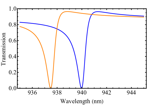
Let us note that the shift is relatively modest owing to the piezoelectric transducer and geometry used for this device, which was not optimized for this purpose, but rather for optomechanical applications in which preservation of the high quality factor of the mechanical resonances requires minimizing clamping losses as much as possible [48, 49]. The 6 mm-inner diameter of the piezoelectric ring actuator was thus chosen only slightly smaller than the 7 mm chip diagonal dimension. For photonics applications, such as low loss tunable optical filters and waveplates, much larger shifts could in principle be obtained by increasing the compression force and optimizing the position of the grating with respect to the piezoelectric transducer. For instance, using larger membrane windows and/or different actuation geometry, as in e.g. [37], could readily yield grating period changes of several nanometers. Second, the optical quality factor of the Fano resonance used here is not particularly high (). Making use of subwavelength gratings with much higher optical quality factor resonances ( was reported in [43]) would readily improve the switching contrast of such a filter. For instance, assuming a reasonable ten times larger period change of 3 nm and an optical Q of would give and a switching contrast of about 10 dB. To verify this, the results of RCWA simulations of the transmission of an infinite SG with , nm, nm and nm with and without a compression corresponding to such a 3 nm grating period change are shown in Fig. 5.
Finally, let us mention that the use of a high optical Q subwavelength grating, even with modest electrical tunability, as the flexible end-mirror of an ultrashort cavity would be interesting for investigating new regimes of cavity optomechanics with strongly-wavelength dependent reflectors [28, 53].
5 Conclusion
The possibility to directly pattern one-dimensional subwavelength gratings on commercial, high-stress, 200 nm-thick suspended silicon nitride films was demonstrated. An enhancement of the reflectivity from 10% to 78% was observed for 937 nm TM polarized light focused on a m2 grating. The broadening and non-zero minimal transmission of the Fano resonance observed in the transmission spectrum were discussed based on RCWA simulations and using transverse profile images of the grating obtained by FIB cutting. Increasing the patterned area and further optimizing of the writing/etching process using the FIB cutting method are expected to reduce collimation broadening and finite grating size effects, and thereby increase the reflectivity. Fine tunability of the optical spectrum by piezoelectric contraction of the suspended film was furthermore evidenced. Such enhanced and electrically tunable reflectivity membranes would be interesting for investigations of collective phenomena in optomechanical arrays of nanomembranes as well as for a number of photonics and optical sensing applications.
Acknowledgments
We are grateful to Pia Bomholt Jensen for assistance with FIB cutting and Folmer Lyckegaard for assistance with gold coating, and acknowledge support from the Velux Foundations, the Danish Council for Independent Research (Sapere Aude initiative) and the Carlsberg Foundation.
References
- [1] Thompson J D, Zwickl B M, Jayich A M, Marquardt F, Girvin S M and Harris J G E 2008 Nature 452 72–75 URL https://doi.org/10.1038/nature06715
- [2] Jayich A M, Sankey J C, Zwickl B M, Yang C, Thompson J D, Girvin S M, Clerk A A, Marquardt F and Harris J G E 2008 New Journal of Physics 10 095008 URL https://doi.org/10.1088/1367-2630/10/9/095008
- [3] Wilson D J, Regal C A, Papp S B and Kimble H J 2009 Phys. Rev. Lett. 103(20) 207204 URL http://link.aps.org/doi/10.1103/PhysRevLett.103.207204
- [4] Camerer S, Korppi M, Jöckel A, Hunger D, Hänsch T W and Treutlein P 2011 Physical Review Letters 107 223001 ISSN 0031-9007 URL https://doi.org/10.1103/PhysRevLett.107.223001
- [5] Karuza M, Molinelli C, Galassi M, Biancofiore C, Natali R, Tombesi P, Giuseppe G D and Vitali D 2012 New J. Phys. 14 095015 ISSN 1367-2630 URL http://stacks.iop.org/1367-2630/14/i=9/a=095015
- [6] Purdy T P, Peterson R W and Regal C A 2013 Science 339 801–804 ISSN 0036-8075 URL http://science.sciencemag.org/content/339/6121/801
- [7] Sawadsky A, Kaufer H, Nia R M, Tarabrin S P, Khalili F Y, Hammerer K and Schnabel R 2015 Physical Review Letters 114 043601 URL https://doi.org/10.1103/PhysRevLett.114.043601
- [8] Xu H, Mason D, Jiang L and Harris J G E 2016 Nature 80 537 URL http://www.nature.com/nature/journal/v537/n7618/abs/nature18604.html
- [9] Nielsen W H P, Tsaturyan Y, Møller C B, Polzik E S and Schliesser A 2017 Proceedings of the National Academy of Sciences of the United States of America 114 62 URL https://doi.org/10.1073/pnas.1608412114
- [10] Kemiktarak U, Metcalfe M, Durand M and Lawall J 2012 Applied Physics Letters 100 061124 (Preprint https://doi.org/10.1063/1.3684248)
- [11] Kemiktarak U, Durand M, Metcalfe M and Lawall J 2012 New J. Phys. 14 125010 ISSN 1367-2630 URL http://stacks.iop.org/1367-2630/14/i=12/a=125010
- [12] Bui C H, Zheng J, Hoch S W, Lee L Y T, Harris J G E and Wong C W 2012 Applied Physics Letters 100 021110 URL https://doi.org/10.1063/1.3658731
- [13] Stambaugh C, Xu H, Kemiktarak U, Taylor J and Lawall J 2015 Annalen der Physik 527 81–88 ISSN 1521-3889 URL http://dx.doi.org/10.1002/andp.201400142
- [14] Bernard S, Reinhardt C, Dumont V, Peter Y A and Sankey J C 2016 Opt. Lett. 41 5624–5627 URL http://ol.osa.org/abstract.cfm?URI=ol-41-24-5624
- [15] Norte R A, Moura J P and Gröblacher S 2016 Physical Review Letters 116(14) 147202 URL https://link.aps.org/doi/10.1103/PhysRevLett.116.147202
- [16] Reinhardt C, Müller T, Bourassa A and Sankey J C 2016 Phys. Rev. X 6(2) 021001 URL http://link.aps.org/doi/10.1103/PhysRevX.6.021001
- [17] Chen X, Chardin C, Makles K, Caër C, Chua S, Braive R, Robert-Philip I, Briant T, Cohadon P F, Heidmann A, Jacqmin T and Deléglise S 2017 Light: Science & Applications 6 e16190 URL http://dx.doi.org/10.1038/lsa.2016.190
- [18] ao P Moura J, Norte R A, Guo J, Schäfermeier C and Gröblacher S 2018 Opt. Express 26 1895–1909 URL http://www.opticsexpress.org/abstract.cfm?URI=oe-26-2-1895
- [19] Bhattacharya M and Meystre P 2008 Phys. Rev. A 78(4) 041801 URL http://link.aps.org/doi/10.1103/PhysRevA.78.041801
- [20] Hartmann M J and Plenio M B 2008 Phys. Rev. Lett. 101(20) 200503 URL http://link.aps.org/doi/10.1103/PhysRevLett.101.200503
- [21] Xuereb A, Genes C and Dantan A 2012 Phys. Rev. Lett. 109(22) 223601 URL http://link.aps.org/doi/10.1103/PhysRevLett.109.223601
- [22] Xuereb A, Genes C, Pupillo G, Paternostro M and Dantan A 2014 Phys. Rev. Lett. 112(13) 133604 URL http://link.aps.org/doi/10.1103/PhysRevLett.112.133604
- [23] Li J, Xuereb A, Malossi N and Vitali D 2016 Journal of Optics 18 084001 URL http://stacks.iop.org/2040-8986/18/i=8/a=084001
- [24] Nair B, Xuereb A and Dantan A 2016 Phys. Rev. A 94(5) 053812 URL http://link.aps.org/doi/10.1103/PhysRevA.94.053812
- [25] Piergentili P, Catalini L, Bawaj M, Zippilli S, Malossi N, Natali R, Vitali D and Giuseppe G D 2018 New Journal of Physics 20 083024 URL http://stacks.iop.org/1367-2630/20/i=8/a=083024
- [26] Brückner F, Friedrich D, Clausnitzer T, Britzger M, Burmeister O, Danzmann K, Kley E B, Tünnermann A and Schnabel R 2010 Phys. Rev. Lett. 104(16) 163903 URL https://link.aps.org/doi/10.1103/PhysRevLett.104.163903
- [27] Guo J, Norte R A and Gröblacher S 2017 Opt. Express 25 9196–9203 URL http://www.opticsexpress.org/abstract.cfm?URI=oe-25-8-9196
- [28] Naesby A and Dantan A 2018 Opt. Express 26 29886–29894 URL http://www.opticsexpress.org/abstract.cfm?URI=oe-26-23-29886
- [29] Huang M C Y, Zhou Y and Chang-Hasnain C J 2008 Nature Photonics 2 180 URL http://dx.doi.org/10.1038/nphoton.2008.3
- [30] Kemiktarak U, Durand M, Metcalfe M and Lawall J 2014 Phys. Rev. Lett. 113(3) 030802 URL https://link.aps.org/doi/10.1103/PhysRevLett.113.030802
- [31] Yang W, Gerke S A, Ng K W, Rao Y, Chase C and Chang-Hasnain C J 2015 Scientific Reports 5 13700 URL http://dx.doi.org/10.1038/srep13700
- [32] Chang-Hasnain C J and Yang W 2012 Adv. Opt. Photon. 4 379–440 URL http://aop.osa.org/abstract.cfm?URI=aop-4-3-379
- [33] Zhou W, Zhao D, Shuai Y C, Yang H, Chuwongin S, Chadha A, Seo J H, Wang K X, Liu V, Ma Z and Fan S 2014 Progress in Quantum Electronics 38 1 – 74 ISSN 0079-6727 URL http://www.sciencedirect.com/science/article/pii/S0079672714000020
- [34] Miroshnichenko A E, Flach S and Kivshar Y S 2010 Rev. Mod. Phys. 82(3) 2257–2298 URL https://link.aps.org/doi/10.1103/RevModPhys.82.2257
- [35] Quaranta G, Basset G, Martin O J F and Gallinet B Laser & Photonics Reviews 12 1800017 (Preprint https://onlinelibrary.wiley.com/doi/pdf/10.1002/lpor.201800017) URL https://onlinelibrary.wiley.com/doi/abs/10.1002/lpor.201800017
- [36] Gärtner C, Moura J P, Haaxman W, Norte R A and Gröblacher S 2018 Nano letters 18 7171–7175 ISSN 1530-6984 URL https://www.ncbi.nlm.nih.gov/pubmed/30247926
- [37] Wang Y, Stellinga D, Klemm A B, Reardon C P and Krauss T F 2015 IEEE Journal of Selected Topics in Quantum Electronics 21 108–113 ISSN 1077-260X
- [38] Ierardi V, Becker U, Pantazis S, Firpo G, Valbusa U and Jousten K 2014 Measurement 58 335 – 341 ISSN 0263-2241 URL http://www.sciencedirect.com/science/article/pii/S0263224114003972
- [39] Mutlu M, Akosman A E, Kurt G, Gokkavas M and Ozbay E 2012 Opt. Express 20 27966–27973 URL http://www.opticsexpress.org/abstract.cfm?URI=oe-20-25-27966
- [40] Fattal D, Li J, Peng Z, Fiorentino M and Beausoleil R G 2010 Nature Photonics 4 466 URL http://dx.doi.org/10.1038/nphoton.2010.116
- [41] Lu F, Sedgwick F G, Karagodsky V, Chase C and Chang-Hasnain C J 2010 Opt. Express 18 12606–12614 URL http://www.opticsexpress.org/abstract.cfm?URI=oe-18-12-12606
- [42] Klemm A B, Stellinga D, Martins E R, Lewis L, Huyet G, O’Faolain L and Krauss T F 2013 Opt. Lett. 38 3410–3413 URL http://ol.osa.org/abstract.cfm?URI=ol-38-17-3410
- [43] Zhou Y, Huang M C Y and Chang-Hasnain C J 2008 Opt. Express 16 14221–14226 URL http://www.opticsexpress.org/abstract.cfm?URI=oe-16-18-14221
- [44] Schuler L P, Milne J S, Dell J M and Faraone L 2009 Journal of Physics D: Applied Physics 42 133001 URL http://stacks.iop.org/0022-3727/42/i=13/a=133001
- [45] Dong B, Sun C and Zhang H F 2017 IEEE Transactions on Biomedical Engineering 64 4–15 ISSN 0018-9294
- [46] Leinders S M, Westerveld W J, Pozo J, van Neer P L M J, Snyder B, O’Brien P, Urbach H P, de Jong N and Verweij M D 2015 Scientific Reports 5 14328 URL http://dx.doi.org/10.1038/srep14328
- [47] Sinha D 2017 Journal of Applied Physics 121 134501 (Preprint https://doi.org/10.1063/1.4979255) URL https://doi.org/10.1063/1.4979255
- [48] Wu S, Sheng J, Zhang X, Wu Y and Wu H 2018 AIP Advances 8 015209 (Preprint https://doi.org/10.1063/1.5009952) URL https://doi.org/10.1063/1.5009952
- [49] Naserbakht S, Naesby A and Dantan A 2019 Applied Physics Letters 115 061105 (Preprint https://doi.org/10.1063/1.5108788) URL https://doi.org/10.1063/1.5108788
- [50] Nair B, Naesby A and Dantan A 2017 Opt. Lett. 42 1341–1344 URL http://ol.osa.org/abstract.cfm?URI=ol-42-7-1341
- [51] Xuereb A, Genes C and Dantan A 2013 Phys. Rev. A 88(5) 053803 URL http://link.aps.org/doi/10.1103/PhysRevA.88.053803
- [52] Xuereb A, Imparato A and Dantan A 2015 New J. Phys. 17 055013 ISSN 1367-2630 URL http://stacks.iop.org/1367-2630/17/i=5/a=055013
- [53] Černotík O, Dantan A and Genes C 2019 Phys. Rev. Lett. 122(24) 243601 URL https://link.aps.org/doi/10.1103/PhysRevLett.122.243601
- [54] Norcada Inc.
- [55] Germer T Modeled Integrated Scatter Tool version 3.01
- [56] Crozier K B, Lousse V, Kilic O, Kim S, Fan S and Solgaard O 2006 Phys. Rev. B 73(11) 115126 URL https://link.aps.org/doi/10.1103/PhysRevB.73.115126
- [57] Brazas J C and Li L 1995 Appl. Opt. 34 3786–3792 URL http://ao.osa.org/abstract.cfm?URI=ao-34-19-3786
- [58] Saarinen J, Noponen E and Turunen J P 1995 Optical Engineering 34 2560 URL https://doi.org/10.1117/12.208079
- [59] Boye R R and Kostuk R K 2000 Appl. Opt. 39 3649–3653 URL http://ao.osa.org/abstract.cfm?URI=ao-39-21-3649
- [60] Ko Y H and Magnusson R 2018 Optica 5 289–294 URL http://www.osapublishing.org/optica/abstract.cfm?URI=optica-5-3-289