Chiral voltage propagation and calibration in a topolectrical Chern circuit
Abstract
We propose an electric circuit array with topologically protected uni-directional voltage modes at its boundary. Instead of external bias fields or floquet engineering, we employ negative impedance converters with current inversion (INICs) to accomplish a non-reciprocal, time-reversal symmetry broken electronic network we call topolectrical Chern circuit (TCC). The TCC features an admittance bulk gap fully tunable via the resistors used in the INICs, along with a chiral voltage boundary mode reminiscent of the Berry flux monopole present in the admittance band structure. The active circuit elements in the TCC can be calibrated to compensate for dissipative loss.
Introduction. The Chern insulator is the mother state of topological band theory. Originally conceived by Haldane as a tight-binding model of electrons with broken time-reversal symmetry on a hexagonal lattice PhysRevLett.61.2015 , it roots in the Berry phase experienced by the electrons as the Brillouin zone is viewed as a compact parameter space Berry45 ; PhysRevLett.62.2747 . The lattice Chern number is quantized to take integer values, as it counts the total charge of Berry flux monopoles. For a Chern insulator with open boundaries, this implies chiral edge modes which experience topological protection against any kind of disorder and other imperfections, as there is no backscattering. This induces a stronger protection than, for instance, topological insulators, where only elastic backscattering is prohibited by the symmetry-protected topological character. Still, dissipative loss is a severe limitation for Chern insulators, and constitutes the central challenge to realize stable edge mode propagation.
As the Berry phase is a phenomenon of parameter space and does not rely on any property of the phase space of quantum electrons, the Chern insulator suggests itself for a plethora of alternative realizations. Haldane and Raghu employed this insight to propose a Chern insulator in photonic crystals by use of the Faraday effect, where chiral edge modes would manifest as one-way waveguides PhysRevLett.100.013904 . This work inspired the subsequent formulation and realization of Chern bands in magneto-optical photonic crystals PhysRevLett.100.013905 ; marin1 , optical waveguides subject to a magnetic field PhysRevLett.100.023902 or floquet modulation alex1 , ultra-cold atomic gases jotzu , mechanical gyrotropic kalu ; nash ; PhysRevLett.115.104302 and acoustic PhysRevLett.114.114301 ; alu1 systems, as well as, most recently, coupled optical resonators Bandreseaar4005 and exciton polariton metamaterials klembt . The nature and potential technological use of topological chiral edge modes crucially depends on the constituent degrees of freedom, the magnitude of the bulk gap, and the ability to prevent loss from affecting the edge dynamics. In all beforementioned physical systems, the latter is the most challenging aspect since, unless one intends to pump the Chern mode anyway, the edge signal exhibits significant decay despite its topological protection.
In this Article, we propose a Chern circuit which is formed by the admittance band structure of an electric network. As initially accomplished for the circuit analogue of a topological crystalline insulator PhysRevLett.106.106802 ; PhysRevX.5.021031 ; PhysRevLett.114.173902 , topolectrical circuits lee1 ; luling have recently been found to host topological admittance band structures helbig1 of high complexity, including Weyl bands lee1 ; luo ; simon1 as well as higher-order topological insulators imhof1 ; sebi1 . Moving beyond the realm of RLC circuits, the combined time reversal symmetry and circuit reciprocity breaking through negative impedance converters with current inversion (INICs) Chen allow us to formulate a topolectrical Chern circuit (TCC) without external bias fields or floquet engineering. We find topologically protected chiral voltage edge modes which, from the viewpoint of electrical engineering, bear resemblance to a voltage circulator. In contrast to previous Chern band realizations, our arrangement of active circuit elements allows for a recalibration of gain and loss to protect the topological chiral voltage signal from decay.
Topolectrical Chern circuit.
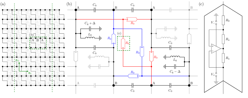
The TCC is formed by a periodic circuit structure sketched in Fig. 1a. The circuit unit cell detailed in Fig. 1b consists of two nodes each of which is connected to three adjacent nodes through a capacitor and to six next-nearest neighbours through INICs supp , which are further characterized in Fig. 1c. As discussed in detail below, these INICs provide the circuit non-reciprocity necessary to induce chiral propagation. The nodes are grounded by inductors as well as capacitors of capacitance on alternating sublattices and . Due to the graph nature of electric circuits implying a gauge degree of freedom for arranging the circuit components in real space helbig1 , we fix the Bravais vectors as and amounting to a brick wall structure shown in Fig. 1a. The grounded circuit Laplacian is defined as the matrix relating the vector of voltages V measured with respect to ground to the vector of input currents I at the circuit nodes by . For an AC frequency and two-dimensional reciprocal space implied by the brick wall gauge, the TCC Laplacian lee1 and its corresponding spectrum of eigenvalues reads
| (1) | ||||
| (2) |
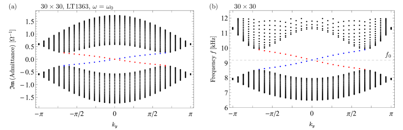
where . In Fig. 2a, we show the projected band structure employing open-boundary conditions in -direction, as specified in Fig. 1a. It features edge-localized chiral admittance modes residing in the admittance gap, reminiscent of the chiral energy modes of a Chern insulator. Spectral reflection symmetry of around zero admittance (Fig. 2a) is accomplished for the frequency .
Chiral edge modes. The capacitive grounding parameter appears in (1) as an inversion symmetry breaking term reminiscent of a Semenoff mass PhysRevLett.53.2449 . The topological character of the model roots in the INIC next-nearest neighbour A-A and B-B coupling elements. They break both time-reversal symmetry and circuit reciprocity via the effective implementation of a negative and positive resistance in the forward and reversed direction of the element, respectively supp . INICs with clockwise orientation (Fig. 1b) effectively act as a voltage circulator, where a voltage profile can only travel in one direction supp . This implements a circular motion of voltage in the bulk of the TCC with no effective translational propagation in any direction. The INIC couplings on different sublattices are oriented such that they break chiral symmetry, and introduce a Haldane mass . By formal comparison to the Haldane model, (1) amounts to inducing an effective magnetic flux of PhysRevLett.61.2015 . It is possible to precisely control this fictitious magnetic flux in the TCC by a modification of the impedance phase of the circuit elements in the INIC (Fig. 1c). The Haldane mass induces a gapped bulk admittance spectrum with chiral edge modes in the admittance gap (Fig. 2a).
Symmetries.
The incorporation of resistances in a circuit environment, such as in the TCC, breaks time-reversal symmetry (TRS) supp . From the viewpoint of thermodynamics, this is because any resistive component experiences Joule heating, leading to increased entropy as well as broken time-reversal symmetry. TRS translates into in real space and in reciprocal space supp . We define circuit reciprocity as given by in real space and by in reciprocal space supp . By the use of operational amplifiers marin2 as active circuit elements, the INIC configuration acts as a charge source or sink, causing an input or output current from ground to the system. Our current feed from the INIC is arranged such that currents between two connected voltage nodes retain equal magnitude, but flow in opposite directions. This yields an antisymmetric contribution to and breaks reciprocity.
We name the TCC Hermitian if and only if is anti-Hermitian, i.e., , which leads to purely imaginary admittance eigenvalues, and hence real eigenfrequencies supp . The stationary time evolution of a given TCC initial state is then conveniently expressed in terms of TCC energy eigenmodes. is intimately connected to its Hamiltonian formulation, as the eigenfrequencies are given by the poles of the Greens function , and hence relate to the roots of the admittance spectrum (Fig. 2b).
Topological phase diagram. We define the Chern number for the lower admittance band where denotes the Berry curvature supp . It is invariant under a change of the Bravais vector gauge, whose only consequence is a distortion of the Brillouin zone helbig1 . As for the Haldane model, from gapping out the two admittance Dirac cones due to finite Haldane or Semenoff mass, there is a topologically non-trivial regime with and a trivial regime with . We find
| (3) |
which is nonzero if . In this case, placing oneself in the admittance or eigenfrequency gap, and allowing for a boundary termination, one finds a chiral mode located at the boundary (Fig. 2a and Fig. 2b). The chiral voltage boundary mode relates to associated with the breaking of circuit reciprocity supp .
Circuit simulations. The TCC in principle allows for a detailed characterization and calibration of the chiral voltage boundary mode. Even for a physical system as accessible and tunable as electric circuits, however, various types of imperfections have to be taken into account to move from an ideal theoretical model to a realistic setting. This includes circuit element variances, parasitic resistances, and other constraints on realistic operational amplifiers we use in the INICs. The principal time scales and parametric dependencies of the chiral edge mode can be deduced from the clean TCC limit (2), where we set . Within linear approximation of the edge mode in the frequency spectrum (Fig. 2b), the group velocities of the zigzag () and bearded edge () yield . As seen from (2), the inverse resistance serves as a regulation parameter of the gap size. Numerical analysis indicate, that for significantly small values of (such that is not significantly larger than unity), the edge mode localization length (understood in units of the internodal spacing) is tunable through the resistance in the INIC.
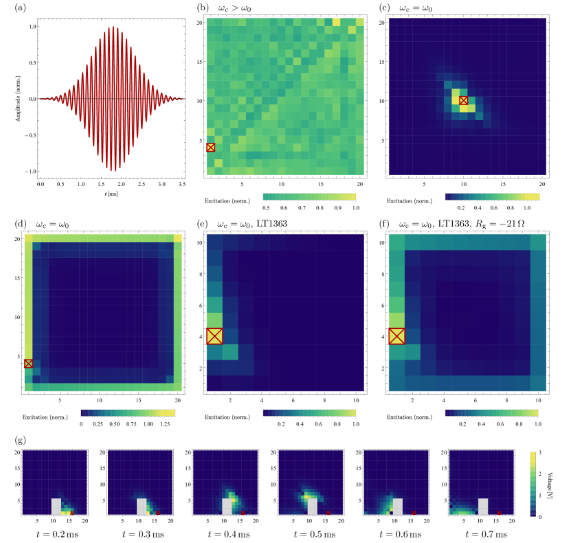
We create a finite TCC lattice, excite it with a Gaussian AC current signal centered around and a standard deviation , and perform LTspice simulations on various configurations (Fig. 3). If, as in Fig. 3b, lies within the TCC frequency band, the current spreads across the whole circuit, even if it is injected at the boundary (marked by a crossed square). If, however, lies within the bulk gap and is sufficiently small, the circuit response is crucially different depending on whether the current is injected in the bulk (Fig. 3c) or at the boundary (Fig. 3d). While it is localized for the former, the signal propagates through the chiral edge mode along the boundary for the latter. Note that due to parasitic effects introduced by the serial resistances of inductors and capacitors , the voltage pulse in the circuit faces dissipation caused by the shift of the resonance frequency spectrum along the positive imaginary axis. The most relevant parasitic effects derive from the inductor, introducing a timewise exponential decay constant that damps the chiral voltage signal. This realistic analysis is further refined in Fig. 3e and Fig. 3f, where we study no idealized, but explicit, publicly available operational amplifier elements LT1363. As seen in Fig. 3e, the realistic setting experiences significant signal decay already across 10 unit cells. In Fig. 3f, we illustrate one way to calibrate the TCC towards a more stable edge signal by adding INIC connections of effective negative resistance between the edge nodes and ground, which effectively yields the insertion of a gain parameter to the system. Through the adjustment of the resistive components in the INICs connected to ground, one can conveniently calibrate the given TCC realization closer towards its Hermitian point, which enhances the Chern mode signal. This is only one of several ways to improve the TCC Chern signal through an inherent TCC parameter adjustment. Such a type of gain implementation to compensate for dissipative loss has not been accomplished in other Chern systems. In Fig. 3f, we implement a defect (grey) at the boundary of the circuit, e.g. by grounding the corresponding voltage nodes. In a time-resolved simulation, we observe a propagation of the edge mode around this defect area. It demonstrates the topological protection of the chiral edge mode, which roots in the existence of a nonzero admittance Chern number as a bulk property.
Conclusion. We have introduced and analyzed the topolectrical Chern circuit as a topological circuit array with active INIC circuit elements. A topological voltage Chern mode appears due to the non-reciprocity induced by the INICs, which at the same time also serve as a convenient calibration tool to minimize the dissipative loss of the edge mode. This reaches an unprecedented level at which a topological chiral edge mode is tunable and analyzable in all detail in an accessible physical environment, and offers itself to further analysis of topological circulator devices in general.
I Acknowledgments
Acknowledgements.
We thank S. Imhof and A. Stegmaier for helpful discussions. The circuit simulations have been performed by the use of LTspice , http://www.linear.com/LTspice. The work in Würzburg is supported by the European Research Council (ERC) through ERC-StG-Thomale-TOPOLECTRICS-336012 and by the German Research Foundation (DFG) through DFG-SFB 1170, project B04.References
- (1) F. D. M. Haldane, Phys. Rev. Lett. 61, 2015 (1988).
- (2) M. V. Berry, Proceedings of the Royal Society of London A: Mathematical, Physical and Engineering Sciences 392, 45 (1984).
- (3) J. Zak, Phys. Rev. Lett. 62, 2747 (1989).
- (4) F. D. M. Haldane and S. Raghu, Phys. Rev. Lett. 100, 013904 (2008).
- (5) Z. Wang, Y. D. Chong, J. D. Joannopoulos, and M. Soljačić, Phys. Rev. Lett. 100, 013905 (2008).
- (6) Z. Wang, Y. Chong, J. D. Joannopoulos, and M. Soljačić, Nature 461, 772 (2009).
- (7) Z. Yu, G. Veronis, Z. Wang, and S. Fan, Phys. Rev. Lett. 100, 023902 (2008).
- (8) M. C. Rechtsman, J. M. Zeuner, Y. Plotnik, Y. Lumer, D. Podolsky, F. Dreisow, S. Nolte, M. Segev, and A. Szameit, Nature 496, 196 (2013).
- (9) G. Jotzu, M. Messer, R. Desbuquois, M. Lebrat, T. Uehlinger, D. Greif, and T. Esslinger, Nature 515, 237 (2014).
- (10) C. L. Kane and T. C. Lubensky, Nature Physics 10, 39 (2013).
- (11) L. M. Nash, D. Kleckner, A. Read, V. Vitelli, A. M. Turner, and W. T. M. Irvine, Proceedings of the National Academy of Sciences of the United States of America 112, 14495 (2015).
- (12) P. Wang, L. Lu, and K. Bertoldi, Phys. Rev. Lett. 115, 104302 (2015).
- (13) Z. Yang, F. Gao, X. Shi, X. Lin, Z. Gao, Y. Chong, and B. Zhang, Phys. Rev. Lett. 114, 114301 (2015).
- (14) A. B. Khanikaev, R. Fleury, S. H. Mousavi, and A. Alù, Nature Communications 6, 8260 (2015).
- (15) M. A. Bandres, S. Wittek, G. Harari, M. Parto, J. Ren, M. Segev, D. N. Christodoulides, and M. Khajavikhan, Science (2018).
- (16) S. Klembt, T. H. Harder, O. A. Egorov, K. Winkler, R. Ge, M. A. Bandres, M. Emmerling, L. Worschech, T. C. H. Liew, M. Segev, C. Schneider, and S. Höfling, arXiv:1808.03179.
- (17) L. Fu, Phys. Rev. Lett. 106, 106802 (2011).
- (18) J. Ningyuan, C. Owens, A. Sommer, D. Schuster, and J. Simon, Phys. Rev. X 5, 021031 (2015).
- (19) V. V. Albert, L. I. Glazman, and L. Jiang, Phys. Rev. Lett. 114, 173902 (2015).
- (20) C. H. Lee, S. Imhof, C. Berger, F. Bayer, J. Brehm, L. W. Molenkamp, T. Kiessling, and R. Thomale, Communications Physics 1, 39 (2018).
- (21) L. Lu, Nature Physics 14, 875 (2018).
- (22) T. Helbig, T. Hofmann, C. H. Lee, R. Thomale, S. Imhof, L. W. Molenkamp, and T. Kiessling, arXiv:1807.09555.
- (23) K. Luo, R. Yu, and H. Weng, Research 2018, 6793752 (2018).
- (24) Y. Lu, N. Jia, L. Su, C. Owens, G. Juzliunas, D. I. Schuster, and J. Simon, arXiv:1807.05243.
- (25) S. Imhof, C. Berger, F. Bayer, J. Brehm, L. W. Molenkamp, T. Kiessling, F. Schindler, C. H. Lee, M. Greiter, T. Neupert, and R. Thomale, Nature Physics 14, 925 (2018).
- (26) M. Serra-Garcia, R. Süsstrunk, and S. D. Huber, arXiv:1806.07367.
- (27) W.-K. Chen, The Circuits and Filters Handbook, 3rd ed. (CRC Press, Inc., Boca Raton, FL, USA, 2009).
- (28) see Supplementary Information.
- (29) G. W. Semenoff, Phys. Rev. Lett. 53, 2449 (1984).
- (30) Z. Wang, Z. Wang, J. Wang, B. Zhang, J. Huangfu, J. D. Joannopoulos, M. Soljačić, and L. Ran, Proceedings of the National Academy of Sciences 109, 13194 (2012).
- (31) H. Shen, B. Zhen, and L. Fu, Phys. Rev. Lett. 120, 146402 (2018).
Appendix A Appendix A: Negative impedance converter (INIC)
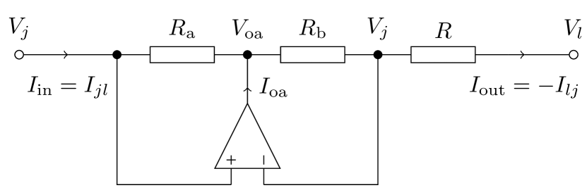
For the realization of a negative impedance converter with current inversion Chen , we use an operational amplifier (OpAmp) configuration shown in Fig. 4. The current entering the INIC from the left is given by , and the current leaving on the right by when the OpAmp is operated in a negative feedback configuration. Assuming an infinite impedance of the OpAmp inputs forbids any current flowing into the OpAmp and simplifies the output current to . Solving these equations for yields
| (4a) | ||||
| (4b) | ||||
Translating those results to the Laplacian form leads to the node voltage equation
| (5) |
where . The matrix is not symmetric, and circuit reciprocity is thus broken. To obtain an anti-Hermitian form as desired in the TCC, we require , i.e. . If this is not the case, the eigenfrequencies of the system become complex, resulting in either a damping or an instability. While the former is manageable, active elements such as OpAmps always necessitate a careful setup such that the active feed does not lead to a divergence, and hence breakdown of the circuit. In mathematical terms, the eigenfrequencies should always be adjusted such that their imaginary part is positive. In a real experiment, it hence needs to be ensured that the system operates stable, i.e. accepting a certain overall loss in order to avoid instabilities. Parasitic effects may in fact help to shift the circuit towards the stable regime. Since electric circuits are so easily tunable, and e.g. resistors can be implemented by individually adjustable potentiometers, the interplay between robust stability and low dissipation can be fine-tuned to the desired optimal Hermitian TCC sweet spot.
Appendix B Appendix B: Hamiltonian formulation
We define voltage and current vectors by denoting the voltages measured at the nodes of a circuit board against ground, and the input currents at the nodes by -component vectors V and I, respectively. The equations of motion of the circuit are given by
| (6) |
where capacitance , conductance , and inductance are the real-valued ()-matrices forming the grounded circuit Laplacian lee1 by
| (7) |
The homogeneous equations of motion (, where the circuit’s time evolution is solely determined by its eigenfrequencies) can be re-written as differential equations of first order
| (8) |
where , i.e., the voltages and their first time derivatives are treated as independent variables. This defines the -Hamiltonian block matrix
| (9) |
where, for the TCC in reciprocal space as in Eq. 1,
| (10a) | ||||
| (10b) | ||||
| (10c) | ||||
The time evolution of a given eigenstate yields where the eigenvalues , are the resonance frequencies of the system (Fig. 2b), defined as the roots of the admittance eigenvalues . To render the measurable voltage V and its time derivative real, the eigenfrequencies of the Hamiltonian must occur in pairs of corresponding to complex conjugated pairs of eigenstates , . This enables us to label the eigenvalues by with and . In Bloch form we label the eigenfrequencies by their corresponding wavenumber k and band index as a composite index . This mapping from wave numbers to frequencies as eigenvalues of the Hamiltonian defines the frequency spectrum in reciprocal space. Due to the intimate connection of the Laplacian and Hamiltonian spectrum, the emergence of a band gap in the admittance band structure is accompanied by an analogous gap opening in the frequency spectrum (Fig. 2). The eigenvectors of the Hamiltonian can be constructed out of the eigenvectors of the Laplacian according to
| (11) |
These are right eigenvectors. Note that the left eigenvectors of the non-Hermitian Hamiltonian may differ.
Appendix C Appendix C: Symmetries
Written in the form of (7), it becomes clear that the Laplacian is anti-Hermitian if and only if and are Hermitian matrices while must be anti-Hermitian, which is fulfilled for the ideal TCC Laplacian.
Time reversal is defined as the parametric operation . As a consequence, voltages transform even and currents odd under time reversal. Concluding from the time-reversed form of (6), we call a circuit time reversal symmetric (TRS) if , which is equivalent to excluding any resistive component in the circuit, where energy can dissipate. This condition can be reformulated as allowing only for fully imaginary real space Laplacians, and is in accordance with the TRS condition in real space defined in the main text, which can be checked by insertion into (7). Translated into reciprocal space, the TRS condition yields .
As a visualization of circuit reciprocity, consider two voltage nodes of the circuit with labels and connected by a passive circuit element. The current flowing out of node must be the current entering at node . In other words, the current running from to , , is the negative of the current running from to , i.e. . This behaviour is called circuit reciprocity. In the Laplacian formalism, circuit reciprocity is given by or in real space, and by in Bloch form. In the present implementation, we use operational amplifiers as active circuit elements in an INIC configuration to tune the system to the point where for the INIC connection. Other implementations of broken circuit reciprocity use magnetic fields or sophisticated transistor arrays such as in passive circulators developed for electrical communication engineering. Based on the fact that the resonance frequencies for are identical to the eigenvalues of the Hamiltonian, we obtain for the frequency spectrum. The voltage eigenmodes of a periodic system are constructed out of Bloch waves in reciprocal space and retrieve the form of plane waves labeled by the wave number k,
| (12) |
For the following considerations, we assume a Hermitian circuit system. If it is additionally TRS and reciprocal, the eigenmodes for inverse k are characterized by
| (13) |
by using and . The eigenmodes to travel in the opposite direction than the ones corresponding to k, and ultimately combine to standing waves that experience no propagation in any direction in a steady-state solution of the system. A propagation can only be induced by breaking the symmetry , which is solely possible by a combined breaking of time reversal symmetry and reciprocity. As detailed in the main text, the INIC configuration implemented as the next-nearest neighbor hopping element breaks time reversal symmetry and reciprocity simultaneously, inducing unidirectional propagation in one direction along the boundary of the TCC in the topological regime.

The states associated with the midgap admittance and frequency bands in Fig. 2a and Fig. 2b of the main text are localized at opposing edges of the circuit due to the breaking of chiral symmetry through the mass term defined in the main text. In the TCC model, establishes the nontrivial topology through next-nearest neighbor INIC connections in a three node arrangement as seen in Fig. 1b and in a more highlighted form in Fig. 5. The associated breaking of reciprocity is caused by a circular motion of voltage in the bulk of the TCC. To physically explain this behaviour, consider three nodes in Fig. 5 with corresponding voltages . In this setting, a current flows out of INIC and , but into from both sides, respectively as depicted in Fig. 5. This way, the current flows from both sides into node , and surpasses the voltage , such that INIC now acts as a current drain and current flows out of node in both directions. Consequently, will fall below , and a new configuration is reached. The voltage has thereby traveled in a clockwise direction as indicated by the orientation of the INICs in Fig. 5. This process will continuously repeat such that a circular motion of voltage in this triangular INIC connection is established, thereby breaking chiral symmetry and reciprocity. The corresponding eigenmodes attain a chiral character, and while applying open boundary conditions, it becomes possible to initiate a voltage wave packet at the boundary of the TCC, which travels along the edge of the circuit in one direction.
Appendix D Appendix D: Hermitian TCC limit
Lemma.
Let a circuit network consist of nodes described by a circuit Laplacian in real space, which can be divided into contributions of different circuit elements according to (7). Moreover, let all capacitances and inductances in the Laplacian be positive. If the Laplacian matrix is anti-Hermitian, for all real frequencies , then the eigenfrequencies of the corresponding Hamiltonian (9) are real.
Proof.
If , it means that , and . Consider the quadratic forms
| (14a) | |||
| (14b) | |||
| (14c) | |||
which are real for all complex -vectors V, since the representing matrices are Hermitian. Assuming only positive capacitances and inductances in the system, the structure of the Laplacian matrices dictates that and are weakly diagonally dominant. Moreover, all entries of the matrices are real, and the diagonal elements are non-negative. Therefore, the matrices are positive semi-definite and .
Now assume that is an eigenvector of the Hamiltonian to eigenvalue . Then the equation
| (15) |
must hold. For the non-trivial cases and , we can solve the quadratic equation for the eigenfrequency by completing the square. We obtain
| (16) |
which is real, because all components are real-valued and , are nonnegative.
Appendix E Appendix E: Berry phase in Hamiltonian and Laplacian form
The Chern number as a topological invariant is defined for the Hamiltonian as the generator of time translation. In the following, we show that for a time-independent, Hermitian system, , the Berry phase and the Chern number, which determine the topological phase of the system, can be identically computed using the Laplacian eigenvectors. Consider the Berry connection defined as
| (17) |
Here, the s are the right eigenvectors of the Hamiltonian. Although the system is Hermitian (, the left eigenvectors of the Hamiltonian may differ from the right eigenvectors. The latter can be expressed using the eigenvectors of the Laplacian,
| (18) |
where the are assumed to be normalized, such that is the normalization of the Hamiltonian eigenvectors. Computing the derivative of the eigenvector while omitting the band indices that are irrelevant for the computation yields
| (19) |
The projection of this result on , exploiting the normalization of the Laplacian eigenvectors, reads
| (20) |
Since , the first and last term in the bracket cancel, and we eventually find
| (21) |
That means that the Berry connection and therefore the Berry curvature and Chern number for the (right) Hamiltonian and Laplacian eigenvectors coincide. Note that the left eigenvectors or right and left eigenvectors of combined may give alternative Berry connections and curvatures. However, the associated Chern numbers are equal PhysRevLett.120.146402 . In this regard, the admittance and frequency band structure of a Hermitian system is topologically equivalent, and we can define the admittance Chern number as the global topological invariant of a circuit system.
Appendix F Appendix F: Low-admittance TCC expansion
The TCC Laplacian in its two-band Bloch from in (1) of the main text can be recast in terms of the Pauli matrices , and as ,
| (22a) | ||||
| (22b) | ||||
| (22c) | ||||
| (22d) | ||||
It features an inversion symmetry breaking Semenoff mass and a reciprocity and time reversal symmetry breaking Haldane mass , which both open a band gap due to their appearance in . We can compute the effective low admittance theory at the Dirac cones at and by expanding up to first order in q as
where the -signs represent the positive and negative chirality of the Dirac cones with admittance gapping mass terms of , respectively. To establish more of a form invariance to the conventional Dirac form, we implement a linear transformation in via , which being a gauge transformation for the circuit graph manifests as a distortion of the Brillouin zone. Neglecting the term proportional to the unit matrix gives the transformed effective low admittance TCC Laplacian
| (23) |
The sign of the Haldane mass relates to the chirality of the Dirac cones, effectively yielding mass terms with opposing signs at the Dirac cones, while the Semenoff mass stays invariant throughout the whole BZ. The Haldane mass therefore induces a Berry flux monopole to which each Dirac cone contributes one half integer Berry charge. The mapping from the torus to the unit sphere establishes the Chern number as the winding number of the vector as a covering of the unit sphere. In the TCC model, this winding number is for each Dirac cone due to the half covering of the unit sphere by the mappings of for each cone. The Chern number of the admittance band structure defined in a gauge-invariant scheme resorts to the introduction of the Berry curvature
| (24) |
We now illustrate that in a reciprocal or time reversal symmetric system, the Chern number vanishes due to the antisymmetry of the Berry curvature in reciprocal space. For that, recall the condition for the circuit Laplacian of a reciprocal system. This leads to individual constraints on the components of the d-vector
| (25a) | |||
| (25b) | |||
| (25c) | |||
| (25d) | |||
We can then use these conditions to compute the Berry curvature (24) of a reciprocal system for inverse wave vectors
| (26) |
by insertion of (25b) - (25d). In a time-reversal symmetric system, exploiting the condition ,
| (27a) | |||
| (27b) | |||
| (27c) | |||
| (27d) | |||
For Hermitian systems, the conditions (27b) -(27d) equal those for reciprocal systems, because the d-vector must be real. In such a case, (26) is trivially fulfilled. The TCC model is a Hermitian model by construction, which means that while omitting next-nearest neighbor hopping terms, the Chern number must vanish. Only by breaking time-reversal symmetry and reciprocity through the INIC next-nearest neighbor connection can the Chern number be nonzero. From a topological point of view, this establishes the combined breaking of reciprocity and time reversal symmetry in a circuit context as the analogue of time reversal symmetry breaking in a quantum electronic system for which the Haldane model was formulated PhysRevLett.61.2015 .
In Appendix D, we have shown that the Berry phase and, consequently, the Chern number is identical in the Hamiltonian and Laplacian formalism. We can therefore establish the admittance band Chern number as a topological invariant of the circuit dynamics. In our TCC model, we set the phase originating from the effective magnetic flux PhysRevLett.61.2015 in the next-nearest neighbor hopping term to , while in full generality, an arbitrary phase is possible by incorporating the desired complex impedance in the INIC configuration. The value of is the favoured configuration in our context, as it features the largest bandgap. By terminating the circuit in an arbitrary direction, we expect to acquire edge modes that are exponentially localized at the boundary between a topologically nontrivial and trivial regime.
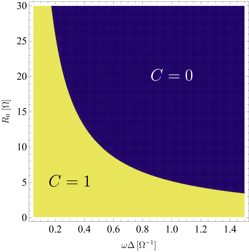
The Chern number for the lower band of the TCC model amounts to the combination of the Chern numbers caused by the half-charged Berry flux monopoles at each Dirac cone
which is nonzero if as mentioned in the main text. In Fig. 6, we show the phase diagram of the TCC model as a function of the capacitive grounding term and the combination of frequency and INIC resistance , which we both restrict to positive values. The topological regime is marked by the Chern number , whereas the topologically trivial phase has vanishing Chern number. As expected, in the limit of , we are always in the topological regime, no matter how we choose . For larger , the parameter needs to be reduced in an inversely proportional fashion to in order to stay in the topological regime. The line of phase transition is determined by the condition .