Electronically Programmable Photonic Molecule
Abstract
Physical systems with discrete energy levels are ubiquitous in nature and are fundamental building blocks of quantum technology. Realizing controllable artificial atom- and molecule-like systems for light would allow for coherent and dynamic control of the frequency, amplitude and phase of photons. In this work, we demonstrate a photonic molecule with two distinct energy-levels and control it by external microwave excitation. We show signature two-level dynamics including microwave induced photonic Autler-Townes splitting, Stark shift, Rabi oscillation and Ramsey interference. Leveraging the coherent control of optical energy, we show on-demand photon storage and retrieval in optical microresonators by reconfiguring the photonic molecule into a bright-dark mode pair. These results of dynamic control of light in a programmable and scalable electro-optic platform open doors to applications in microwave photonic signal processing, quantum photonics in the frequency domain, optical computing concepts and simulations of complex physical systems.
Photonic analogues of condensed matter systems have resulted in important discoveries like photonic crystals Joannopoulos et al. (1997), parity-time symmetric systems Regensburger et al. (2012) and topological photonic systems Lin et al. (2016); Lu et al. (2014), and have led to breakthrough technologies including quantum ground state cooling of nanomechanical systems Chan et al. (2011), new classes of sensors Hodaei et al. (2017); Chen et al. (2017) and one-way lasers Bandres et al. (2018).A photonic analogue of a two-level system could allow full-control over the energy and phase of photons using the concept of two-level systems control in atomic or molecular systems, where the state of the electron can be controlled and functionalized by external electromagnetic fields. Such a photonic system would enable the investigation of complex physical phenomena Joannopoulos et al. (1997); Regensburger et al. (2012); Lu et al. (2014); Bandres et al. (2018); Kues et al. (2017) and unique functionalities, including on-demand photon storage and retrieval, coherent optical frequency shift and optical quantum information processing at room temperature Kues et al. (2017); O’Brien (2007); Liu et al. (2001). However, the fundamental building block, a coherent photonic two-level system that can be programmed and dynamically controlled, is still missing. While realizing a photonic device with discrete energy levels is straightforward, for example using modes of an optical resonator, controlling such a system dynamically is challenging as it requires mixing of optical frequencies via strong nonlinear processes. As a result, coherent coupling between discrete photon energy modes have only been studied using all optical methods Guo et al. (2016); Ramelow et al. (2018); Sato et al. (2012), which require high optical pump powers and have limited design parameter space, configurability and scalability.
Electro-optic methods Capmany and Novak (2007); Xu et al. (2005); Ayata et al. (2017); Wade et al. (2015); Liu et al. (2011); Shambat et al. (2011); Shen et al. (2017) are ideally suited for controlling photonic two-level systems since they have fast response, can be programmed and allow for large scale integration.To realize a fully unitary photonic two-level system with coherent electro-optic control, the photon lifetime of each energy state needs to be much longer than the time required to drive the system from one state to the other. On the one hand, Large optical systems with optical amplifiers Spreeuw et al. (1990) can emulate a classical two-level system but the quantum coherence of the optical photons is destroyed in the process. On the other hand, conventional integrated photonic platforms have not been able to meet the requirements of long photon lifetime and fast modulation simultaneously. For example, fast phase modulators Kues et al. (2017); Karpinski et al. (2017) can generate new optical frequencies but they do not support distinct and long-lived optical modes. On the other hand, ultra-high Q on-chip resonators have traditionally been realized in passive materials, such as silicon dioxide (SiO2) Armani et al. (2003); Lee et al. (2012) and silicon nitride (Si3N4) Ji et al. (2017); Bauters et al. (2011), which can only be controlled electrically using slow thermal effect. Electrically active photonic platforms based on silicon Xu et al. (2005), III-V materials Shambat et al. (2011); Guo et al. (2016), plasmonics Ayata et al. (2017), graphene Liu et al. (2011), and polymers Enami et al. (2007) allow for fast electro-optic modulation at gigahertz frequencies, but suffer from dramatically reduced photon lifetimes compared to passive platforms.
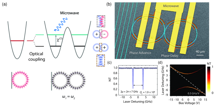
In this work, we overcome the existing performance trade-off paradigm and realize a programmable photonic two-level system that can be dynamically controlled using gigahertz microwave signals (Fig. 1a). Specifically, we create a microwave addressable photonic molecule using a pair of - radius integrated lithium niobate (LN) microring resonators patterned in close proximity to each other (Fig. 1b). The low optical loss Zhang et al. (2017) and the efficient co-integration microwave electrodes Guarino et al. (2007); Witmer et al. (2017) allow us to simultaneously achieve large electrical bandwidth ( 30 GHz), strong modulation efficiency (0.5 GHz/V) and long photon lifetime (2 ns).
The photonic molecule supports a pair of well-defined optical energy levels, which are evident from the optical transmission measured using a tuneable telecom wavelength laser (Fig. 1c; also, see Supplementary for full spectrum). The two optical energy levels are formed by the evanescent coupling of light from one resonator to another through a 500-nm gap. When the optical coupling strength exceeds the optical loss rate of each cavity, the coupling leads to a normal mode splitting resulting in a frequency doublet consisting of a lower frequency symmetric (S) and a higher frequency antisymmetric (AS) optical mode (Fig. 1a and c). The S (AS) mode spatially spans both optical cavities, with the light in the two cavities being in- (out-of-) phase. The two new eigenmodes, separated in frequency by the optical coupling strength, are the energy states of the photonic molecule. In our case, the two optical modes are separated by GHz and have cavity linewidths of MHz, corresponding to a loaded (intrinsic) quality factors of (), thus forming a well-resolved two-level system (Fig. 1c).
We induce photonic transitions in the two-level system using high-frequency electro-optic phase modulation of the two modes. The phase modulation is realized through the Pockels effect () of LN, where the optical refractive index can be changed by an applied electric field, with a response time on the femtosecond scale. To enable strong overlap between microwave and optical fields without significantly increasing the optical loss, we place gold microelectrodes 2.5 away from the edge of the rings that form the photonic molecule (Fig. 1b). Importantly, the microwave circuit layout is designed to induce a phase delay on one ring and a phase advance on the other ring therefore introducing coupling between the spatially orthogonal S and AS modes (Fig. 1a and Supplementary).
We explore the analogy between an atomic two-level system and the photonic two-level system, and leverage it to demonstrate the control of the photonic molecule. We note that in our system the electro-optic effect plays the role equivalent to that of an electric dipole moment in the case of an atomic two-level systems, where in both systems external electromagnetic fields are used to couple and address the energy levels. Building on this analogy, we show that the energy levels of the photonic molecule can be programmed by applying a direct current (DC) electric field, the effect equivalent to a DC Stark shift used to control the energy levels in an atom. This is accomplished by applying a DC bias voltage in the range of 15 V to the microwave electrodes, which results in an avoided crossing curve shown in figure 1d. The extracted tuning/modulation efficiency GHz/V is an order of magnitude larger than previously demonstrated in bulk electro-optic resonator systems Rueda et al. (2016); Savchenkov et al. (2009), and is due to the highly efficient overlap between microwave and optical fields enabled by our system Wang et al. (2018).
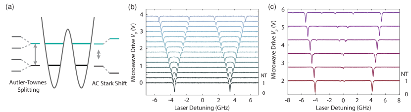
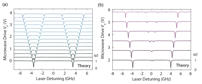
Next, we use a continuous wave (CW) coherent microwave field to control our photonic two-level system. This situation is similar to an atomic two-level system under a strong coherent excitation, with an important difference that in our case the number of photons that could populate each of the two levels is not limited to one, resembling that of an atomic ensemble. When the microwave frequency matches the energy difference of the two levels, an effective coupling between the two initially decoupled S and AS modes is introduced, leading to microwave-induced photonic Autler-Townes splitting (Rabi splitting), shown in Fig. 2a. This is similar to the emergence of dressed states in the case of an atomic two-level system resonantly excited with CW light. In our system, the splitting frequency () can be precisely controlled up to several gigahertz by controlling the amplitude of the microwave signals (Fig. 2b). When the microwave frequency is far detuned from the transition frequency, an effective dispersive effect in the level splitting is induced, analogous to the AC Stark shift in atomic systems (Fig. 2c). Importantly, this effect can be used to control the effective coupling strength between the energy levels of the photonic molecule, which are otherwise determined by geometric factors.
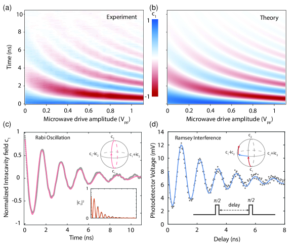
We demonstrate the photonic molecule can be used for unitary transformation of light in the frequency domain using Rabi oscillation and Ramsey interference (see Supplementary). The observed Rabi oscillation corresponds to a rotation along the real axis of the energy Bloch sphere (Fig. 3c, inset) and indicates that light tunnels back and forth between the two optical modes at two different optical frequencies. In other words, using the language of nonlinear optics, applied microwave signal drives a sequence of resonance enhanced sum- and difference-frequency generation (SFG and DFG) processes that result in energy of photons being changed several times (more than 10 in Fig. 3c) before it is eventually dissipated due to the cavity photon loss (cavity life time 1.6 ns). To study the Rabi oscillation, we initialize the system by coupling a CW laser into the S mode and measure the real-time optical transmission as the microwave drive is turned on (see Methods and Supplementary). We find a large range of Rabi frequencies achievable with low applied voltages (Fig. 3a) to be in excellent agreement with theoretical predictions (Fig. 3b and Supplementary). In particular, for a peak drive voltage of V, we observe coherent Rabi oscillation with a frequency of 1.1 GHz, being of the initial mode splitting. Even stronger driving regimes, where the Rabi frequencies are close or even exceed the level splitting, could be accessible in our system, thus enabling exploration of the extreme conditions where the rotating-wave approximation completely breaks down Casanova et al. (2010).
To show the control over the relative phase of the two photonic levels in our system (i.e. rotation along the imaginary axis), we measure photonic Ramsey interference by driving the system with detuned microwave pulses at 7.8 GHz. After initializing the system in the S mode, we apply a microwave pulse to transform the optical field into a superposition of the two states. As the microwave is turned off for a time period of , the superposition state precesses along the equator of the Bloch sphere at a rate determined by the microwave detuning After sending another microwave pulse, the photons are rotated to different energy states, determined by the delay , and measured using a photodetector. The result is the so-called Ramsey interference shown in figure 3d. As the optical lifetime of the two-level system ( 1.6 ns) is much shorter than the coherence time of the laser (s), the phase coherence time of the two energy levels obtained in this measurement is dominated by cavity dissipation in good agreement with that obtained from the Rabi oscillation.
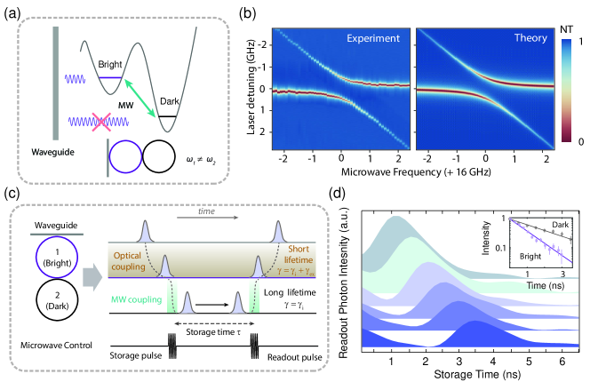
We leverage the ability to perform unitary transformations in the frequency domain to achieve on-demand photon storage and retrieval - a critical task for optical signal processing. While a static resonator can be used to slow down the propagation of a photon, such slow-down is fundamentally limited by the frequency bandwidth of the resonator, i.e. the delay-bandwidth product, and cannot be controlled on-demand. In contrast, the use of a dynamically-modulated resonator system can overcome the delay-bandwidth product constraint, enabling new functionalities such as optical buffering Yanik and Fan (2004). To enable controllable write and read of photons into a resonator and from an external waveguide, the optical coupling strength needs to be altered faster than the cavity photon lifetime. To achieve this, we apply a large DC bias voltage (15 V) to reconfigure the photonic molecule into a pair of bright and dark modes. In this limit, one of the modes is mainly localized in the 1st ring (purple in Fig. 4a), and thus is still accessible to the input optical waveguide and is optically bright, while the other mode is mainly localized in the 2nd ring (black in Fig. 4a) and thus is decoupled from the input optical waveguide by geometry and becomes optically dark (See Supplementary for details). Notably, optical access to the dark optical mode can be granted by applying a microwave signal with frequency matched to the difference between the two optical modes (Fig. 4a). The microwave modulation results in an effective coupling between the bright and the dark mode, which we directly observe from the avoided crossing in the spectrum of the bright optical mode (Fig. 4b). In our experiment, the waveguide coupling is designed to be critically-coupled to a single resonator maximizing the transmission extinction ratio. We excite the critically-coupled bright mode from the optical waveguide, and then apply a microwave pulse to switch light from the bright to the dark mode (Fig.4c). Once the microwave signal is turned off, the photons are trapped in the dark mode and become decoupled from the waveguide leaving cavity intrinsic dissipation as the only photon loss mechanism. After a desired storage time, we apply another microwave pulse to deterministically retrieve the photons from the dark mode back into the bright mode and then into the optical waveguide (Fig. 4c). Tracking the intensity of the retrieved optical pulses stored in the dark mode, we extract a dark mode lifetime of 2 ns, which is about two times of the lifetime of the critically coupled bright mode as expected (Fig. 4d). Using an over-coupled bright optical modes, while further improving the quality factor of the integrated lithium niobate resonators towards its material limit (), could result in a tunable storage time of hundreds of nanoseconds (see Supplementary).
Our demonstration of the coherent and dynamic control of a two-level photonic molecule with microwave fields and on-demand photon storage and retrieval paves a path to a new paradigm of control over photons. These results represent the initial step towards integrated electro-optic coherent manipulation of photonic states and energies, and could have immediate applications in signal processing and quantum photonics. With microwave control and the possible integration of on-chip photonic components including filters, routers and modulators, a new generation of photonic-electronic systems with advanced functionalities can be put in practice. Considering the high versatility and scalability of dynamically controlled two- and multi-level photonic systems, they have the potential to enable novel photonic technologies including topological photonics Lin et al. (2016), advanced photonic computation concepts McMahon et al. (2016); Shen et al. (2017) and on-chip optical quantum systems O’Brien (2007); Kues et al. (2017).
This work was supported in part by National Science Foundation Grant (ECCS1609549, DMR-1231319), Office of Naval Research MURI grant N00014-15-1-2761 and Army Research Laboratory Center for Distributed Quantum Information W911NF1520067, Center for Integrated Quantum Materials (CIQM). Device fabrication was performed at CNS at Harvard University.
References
- Joannopoulos et al. (1997) J. D. Joannopoulos, P. R. Villeneuve, and S. Fan, Nature 386, 143 (1997).
- Regensburger et al. (2012) A. Regensburger, C. Bersch, M.-A. Miri, G. Onishchukov, D. N. Christodoulides, and U. Peschel, Nature 488, 167 (2012).
- Lin et al. (2016) Q. Lin, M. Xiao, L. Yuan, and S. Fan, Nature Communications 7, ncomms13731 (2016).
- Lu et al. (2014) L. Lu, J. D. Joannopoulos, and M. Soljacic, Nature Photonics 8, 821 (2014).
- Chan et al. (2011) J. Chan, T. P. M. Alegre, A. H. Safavi-Naeini, J. T. Hill, A. Krause, S. Groblacher, M. Aspelmeyer, and O. Painter, Nature 478, 89 (2011).
- Hodaei et al. (2017) H. Hodaei, A. U. Hassan, S. Wittek, H. Garcia-Gracia, R. El-Ganainy, D. N. Christodoulides, and M. Khajavikhan, Nature 548, 187 (2017).
- Chen et al. (2017) W. Chen, a. K. Ozdemir, G. Zhao, J. Wiersig, and L. Yang, Nature 548, 192 (2017).
- Bandres et al. (2018) M. A. Bandres, S. Wittek, G. Harari, M. Parto, J. Ren, M. Segev, D. N. Christodoulides, and M. Khajavikhan, Science , eaar4005 (2018).
- Kues et al. (2017) M. Kues, C. Reimer, P. Roztocki, L. R. Cortés, S. Sciara, B. Wetzel, Y. Zhang, A. Cino, S. T. Chu, B. E. Little, D. J. Moss, L. Caspani, J. Azaña, and R. Morandotti, Nature 546, 622 (2017).
- O’Brien (2007) J. L. O’Brien, Science 318, 1567 (2007).
- Liu et al. (2001) C. Liu, Z. Dutton, C. H. Behroozi, and L. V. Hau, Nature 409, 490 (2001).
- Guo et al. (2016) X. Guo, C.-L. Zou, H. Jung, and H. X. Tang, Physical Review Letters 117, 123902 (2016).
- Ramelow et al. (2018) S. Ramelow, A. Farsi, Z. Vernon, S. Clemmen, X. Ji, J. E. Sipe, M. Liscidini, M. Lipson, and A. L. Gaeta, arXiv:1802.10072 [physics, physics:quant-ph] (2018), arXiv: 1802.10072.
- Sato et al. (2012) Y. Sato, Y. Tanaka, J. Upham, Y. Takahashi, T. Asano, and S. Noda, Nature Photonics 6, 56 (2012).
- Capmany and Novak (2007) J. Capmany and D. Novak, Nature Photonics 1, 319 (2007).
- Xu et al. (2005) Q. Xu, B. Schmidt, S. Pradhan, and M. Lipson, Nature 435, 325 (2005).
- Ayata et al. (2017) M. Ayata, Y. Fedoryshyn, W. Heni, B. Baeuerle, A. Josten, M. Zahner, U. Koch, Y. Salamin, C. Hoessbacher, C. Haffner, D. L. Elder, L. R. Dalton, and J. Leuthold, Science 358, 630 (2017).
- Wade et al. (2015) M. T. Wade, X. Zeng, and M. A. Popovic, Optics Letters 40, 107 (2015).
- Liu et al. (2011) M. Liu, X. Yin, E. Ulin-Avila, B. Geng, T. Zentgraf, L. Ju, F. Wang, and X. Zhang, Nature 474, 64 (2011).
- Shambat et al. (2011) G. Shambat, B. Ellis, M. A. Mayer, A. Majumdar, E. E. Haller, and J. Vučković, Optics Express 19, 7530 (2011).
- Shen et al. (2017) Y. Shen, N. C. Harris, S. Skirlo, M. Prabhu, T. Baehr-Jones, M. Hochberg, X. Sun, S. Zhao, H. Larochelle, D. Englund, and M. Soljacic, Nature Photonics 11, 441 (2017).
- Spreeuw et al. (1990) R. J. C. Spreeuw, N. J. van Druten, M. W. Beijersbergen, E. R. Eliel, and J. P. Woerdman, Physical Review Letters 65, 2642 (1990).
- Karpinski et al. (2017) M. Karpinski, M. Jachura, L. J. Wright, and B. J. Smith, Nature Photonics 11, 53 (2017).
- Armani et al. (2003) D. K. Armani, T. J. Kippenberg, S. M. Spillane, and K. J. Vahala, Nature 421, 925 (2003).
- Lee et al. (2012) H. Lee, T. Chen, J. Li, K. Y. Yang, S. Jeon, O. Painter, and K. J. Vahala, Nature Photonics 6, 369 (2012).
- Ji et al. (2017) X. Ji, F. A. S. Barbosa, S. P. Roberts, A. Dutt, J. Cardenas, Y. Okawachi, A. Bryant, A. L. Gaeta, and M. Lipson, Optica 4, 619 (2017).
- Bauters et al. (2011) J. F. Bauters, M. J. R. Heck, D. John, D. Dai, M.-C. Tien, J. S. Barton, A. Leinse, R. G. Heideman, D. J. Blumenthal, and J. E. Bowers, Optics Express 19, 3163 (2011).
- Enami et al. (2007) Y. Enami, C. T. Derose, D. Mathine, C. Loychik, C. Greenlee, R. A. Norwood, T. D. Kim, J. Luo, Y. Tian, A. K.-Y. Jen, and N. Peyghambarian, Nature Photonics 1, 180 (2007).
- Zhang et al. (2017) M. Zhang, C. Wang, R. Cheng, A. Shams-Ansari, and M. Loncar, Optica 4, 1536 (2017).
- Guarino et al. (2007) A. Guarino, G. Poberaj, D. Rezzonico, R. Degl’Innocenti, and P. Gunter, Nature Photonics 1, 407 (2007).
- Witmer et al. (2017) J. D. Witmer, J. A. Valery, P. Arrangoiz-Arriola, C. J. Sarabalis, J. T. Hill, and A. H. Safavi-Naeini, Scientific Reports 7 (2017), 10.1038/srep46313.
- Rueda et al. (2016) A. Rueda, F. Sedlmeir, M. C. Collodo, U. Vogl, B. Stiller, G. Schunk, D. V. Strekalov, C. Marquardt, J. M. Fink, O. Painter, G. Leuchs, and H. G. L. Schwefel, Optica 3, 597 (2016).
- Savchenkov et al. (2009) A. A. Savchenkov, W. Liang, A. B. Matsko, V. S. Ilchenko, D. Seidel, and L. Maleki, Optics Letters 34, 1300 (2009).
- Wang et al. (2018) C. Wang, M. Zhang, B. Stern, M. Lipson, and M. Loncar, Optics Express 26, 1547 (2018).
- Casanova et al. (2010) J. Casanova, G. Romero, I. Lizuain, J. J. Garcia-Ripoll, and E. Solano, Physical Review Letters 105, 263603 (2010).
- Yanik and Fan (2004) M. F. Yanik and S. Fan, Physical Review Letters 92, 083901 (2004).
- McMahon et al. (2016) P. L. McMahon, A. Marandi, Y. Haribara, R. Hamerly, C. Langrock, S. Tamate, T. Inagaki, H. Takesue, S. Utsunomiya, K. Aihara, R. L. Byer, M. M. Fejer, H. Mabuchi, and Y. Yamamoto, Science 354, 614 (2016).
Supplemental Information
I Summary of Fabrication and Measurements Methods
Devices are fabricated on a single crystalline thin-film lithium niobate (LN) device layer bonded onto a silicon (Si) handle wafer with a 2 m thick thermally grown silicon dioxide layer on top. Standard electron-beam (e-beam) lithography is used to realize optical waveguides and microresonator patterns in hydrogen silsequioxane (HSQ) e-beam resist. The patterns are then transferred into the LN layer using argon plasma etching in a standard inductively couple plasma reactive ion etching (ICP-RIE) tool. The etched depth is 350 nm leaving a 250 nm LN slab behind. The slab allows for efficient electrical field penetration into the waveguide core region. The first layer of the gold interconnects is patterned using e-beam lithography and the metals are deposited with e-beam evaporation methods and lift-off processes. Next, a 1.6 m silicon dioxide layer is deposited on top using plasma enhanced physical vapour deposition (PECVD) method. Finally, metal vias and the top metal layer are realized using a standard photolithography followed by e-beam evaporation and lift-off processes.
The light from a tunable telecom wavelength laser (SANTEC TS510) is launched into, and collected from, the LN waveguides using a pair of lensed optical fibres. The microwave control signals are generated from an arbitrary waveform generator (AWG, TEKTRONIX 70001A), before they are sent to electrical amplifiers. Electrical circulator or isolators are used to prevent multiple electrical reflections. For the Rabi oscillation measurements, the electric field amplitude () in the S mode is measured by interfering the light out-coupled from the double-ring system with the pump light in the optical waveguide. The interference produces a homodyne signal for that is sent to a 12 GHz photodiode (Newport 1544A), and due to the optical frequency difference, the rapid interference signal between the pump light and can be filtered out electrically using a low-pass filter. For the Ramsey measurements, the optical power is sampled after the 2nd pulse using the fast photodiode. For the photon storage measurements, the pump light is synchronously turned off with the first pulse allowing for direct power readout of the retrieved light and prevent pump further leaking into the bright mode. The modulation on the pump signal is achieved by an external electro-optic modulator synchronized with the microwave control signals.
II Device and Experimental Setup Details
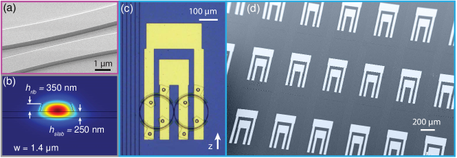
The ring resonators of the photonic molecule have waveguide width of 1.4 m and vary coupling gaps of nm. The coupling waveguides are 800 nm wide by 600 nm thick with a rib height of 350 nm and slab height of 250 nm. This ratio is chosen to ensure optimum electro-optic over-lap while still maintaining a tight bending radius.
The high frequency microwave electrodes are designed to achieve differential driving of the two resonators. As shown in figure S1, the top contact pad is connected to the bottom electrodes of the left ring and the top electrodes of the right ring (and vise versa for the bottom contact pad). Since the LN thin film is -cut (extraordinary axis in plane), such configuration allows the electrical field to be in the same direction on each ring, while opposite for the two rings. Here we pattern 60 programmable photonic molecules on a 10 mm by 8 mm thin film lithium niobate (LN) chip.
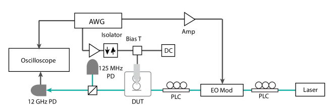
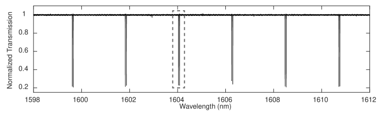
The optical properties of the devices are characterized using a tunable telecom laser (Santec TSL-550). The polarization of the light is tuned to TE (in-plane of the chip) before sending into the chip with a lensed fiber. The DC transmission is measured on a 125 MHz photodetector (New Focus 1811A) and the fast oscillation signal is measured on a 12 GHz photodetector (New Focus 1544A) and a fast real-time oscilloscope (Tektronix MSO71604C). Figure S3 shows the normalized transmission spectrum of the photonic molecule, showing pairs of two-level resonances separated by the free-spectral-range of the microring resonator ( 2.2 nm).
The microwave signals are prepared using an arbitrary waveform generator (Tektronix 70001A), which provides synchronized signals to drive the photonic molecule as well as an external modulator and the oscilloscope. The microwave driving signal for the photonic molecule is amplified and sent through an isolator to minimize reflection to the amplifier. A bias-T is used to coupled DC field into the resonator for fine tuning.
III Description of the photonic molecule
III.1 System Hamiltonian
The nanophotonic two-level system under a coherent microwave drive can be described by a Hamiltonian with the form
| (S1) |
where () and () are the annihilation (creation) operators of the two optical modes of the respective microresonator, is the coupling strength between the two optical resonators, is the interaction strength of microwave field to the optical resonator, determined by the coupling strength and microwave peak amplitude . is the frequency of the microwave modulation.
III.2 Identical resonator: two bright modes
When the resonant frequencies of the two resonators are identical, i.e. , equation (S1) can be expressed as
| (S2) |
where , and .
To simplify the system, we apply a unitary transformation and the rotating wave approximation (RWA), we obtain
| (S3) |
where the microwave detuning and is the frequency difference between and . Equation S3 is equivalent to the time independent Hamiltonian
| (S4) |
We obtain the following equations of motion using input-output theory from equation S4,
| (S5) |
III.3 Autler-Townes Splitting and AC Stark Shifts
Under a continuous wave microwave modulation with frequency close to the optical two-mode splitting, each resonance of will further split into two dips with splitting frequency
| (S6) |
obtained by diagonalizing the coupling matrix from equation S5.
For the Autler-Townes splitting measurement data shown in Fig. 2a in the main text and simulation shown in Fig. S4, the microwave modulation signal is on-resonance with the optical two-mode splitting, i.e. , with .
When the microwave frequency detuning to the two-mode resonances is much larger than the driving strength (i.e. ), the microwave modulation behaves as a weak perturbation. This perturbation induces a shift of the optical energy levels. Applying the second-order perturbation theory, we have
III.4 Optical two-level dynamics
To study the dynamics of the photonic two-level system, we consider the equations of motion S5 with optical loss and laser input fields. For a single tone optical input on resonance with , the equations of motion are:
| (S7) | |||
| (S8) |
where is the total decay rate of the modes , is the waveguide coupling rate to mode and is the input laser field. After dropping the fast rotating terms with frequency of , we obtain the dynamical solution of and ,
| (S9) | ||||
where is the steady state amplitude in mode before the microwave is turned on and is the laser detuning. Here is the Autler-Townes splitting frequency as in equation S6 and is also the Rabi oscillation frequency. The output power from the waveguide is then
| (S10) | ||||
Substitute equations S9 into the expression of the output power and set , we obtain
| (S11) |
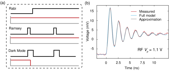
where and we made the approximation to drop the fast rotating terms of at GHz, as we restrict our measurement bandwidth to GHz. The intra-cavity field can therefore be directly calculated from the output intensity by . Therefore the real-time AC signal on the photodetector is directly related to the intracavity field . Figure S5 shows the full numerical solution as of equation S2, the approximated solution S11 and the measured photodetector voltage.
The Ramsey interference is achieved by applying two microwave pulses separated by a time delay . Here the microwave signal is detuned from the level-splitting by . Using the protocol of Ramsey interference and equation S7, S8 , we can get the solution after two pulse as a function of time delay :
| (S12) |
| (S13) |
where from mode . is the duration of the pulse. The first terms in equations S12 and S13 represent the intra-cavity fields exist in the cavity prior to the arrival of the first pulse. The second terms are the leakage of the pump signal into the cavity during the delay, which contributes to a DC term. So the oscillation of the output signal rotating at with the frequency corresponds to the population of after dropping the fast rotating terms related to .
III.5 Optical dark modes
In the case where and are far detuned by , as in the photon storage and retrieval measurements, we prefer to eliminate the coupling term by a Bogoliubov transformation. Assuming a new basis of satisfying:
Since needs to satisfy the bosonic commutation relationship, we have the condition . So we set with . Then result of this transformation gives us a Hamiltonian for :
where . This Hamiltonian indicate that for , the microwave modulation has a component that induces an exchange interaction and a component that induces a frequency modulation .
As for the bright mode pair case we discussed above, i.e. for a small bias , are nearly degenerate and in basis,
whereas in the case of a birght-dark optical mode pair, i.e. the bias voltage is high , have a large frequency difference and in basis, is composed by a large part of with small part of and has large part of while has only small part of . That means:
Here the conversion term is finite and is suppressed by a factor and the term is large, meaning that are being frequency modulated. However, Since the modulation frequency is orders of magnitudes larger than the bandwidth of the optical modes, we can neglect this term under high- approximation. The resulting Hamiltonian still has a similar form to the bright mode pairs, with a pre-factor in conversion efficiency.
| (S14) |
Similar to the previous section, applying RWA and input-output theory to equation S14, we obtain
where , is the internal loss of each ring and is the external loss of ring 1 to waveguide, and are the external losses of modes to waveguide. From these equations of motion, we see that at large bias voltages, and the access of mode to the external waveguide is effectively controlled by the microwave drive . At the same time, the life time for mode becomes closer to that of the intrinsic cavity life time. Therefore, -pulse control sequences can be implemented as described in the main text to achieve the on-demand photon-storage and retrieval.
The bright mode can be over-coupled to the optical waveguide while the dark mode is detuned far from the bright optical mode. As an example, assuming a lithium niboate ring resonator can be fabricated close to its material loss limit (), set GHz, GHz so , and let GHz, one could achieve a tunable delay of more than 800 ns with a minimum of 500 ps steps (limited by output coupling bandwidth) and over efficiency.