title
Automated Netlist Generation for 3D Electrothermal and Electromagnetic Field Problems
Abstract
We present a method for the automatic generation of netlists describing general three-dimensional electrothermal and electromagnetic field problems. Using a pair of structured orthogonal grids as spatial discretisation, a one-to-one correspondence between grid objects and circuit elements is obtained by employing the finite integration technique. The resulting circuit can then be solved with any standard available circuit simulator, alleviating the need for the implementation of a custom time integrator. Additionally, the approach straightforwardly allows for field-circuit coupling simulations by appropriately stamping the circuit description of lumped devices. As the computational domain in wave propagation problems must be finite, stamps representing absorbing boundary conditions are developed as well. Representative numerical examples are used to validate the approach. The results obtained by circuit simulation on the generated netlists are compared with appropriate reference solutions.
keywords:
absorbing boundary conditions, circuits, electromagnetics, electrothermal, finite integration technique, netlists.1 Introduction
In order to analyse complex electromagnetic (EM) problems, two main routes can be identified. First, a numerical approach for solving the full set of Maxwell’s field equations offers the advantage of capturing all relevant effects but can be very demanding in terms of computational resources. One of the first methods for EM analysis was the finite difference time domain (FDTD) scheme proposed by Yee [1] in the 1960s. This method became popular and is still a standard approach for high-frequency EM simulations [2]. About ten years later, in the 1970s, Weiland [3] introduced the finite integration technique (FIT) as an extension to the FDTD scheme using integral unknowns and allowing for non-Cartesian and unstructured grids [4]. Additionally, later developments of the method led to the usage of integral unknowns to obtain an exact implementation of Maxwell’s equations [5]. The method proved to be more efficient in terms of memory requirements and computing time. While the finite element method (FEM) was mainly used in structural mechanics for many years, the introduction of edge elements made it applicable for EM problems as well [6]. Secondly, one may use compact models to obtain an efficient representation of a complex system. For example, electrical engineers employ circuits to model and describe the behaviour of complex devices. Nevertheless, the generation of such compact models can be a tedious task requiring empirical know-how to apply the appropriate approximations. To generate such circuit models, different techniques are available. For instance, mathematical analysis and physical insight allows to construct circuits representing the problem at hand as is done by Choi et al [7]. A circuit’s topology and the required component values can also be obtained from experimental results as is done by Moumouni and Baker [8] and other groups. Another approach, e.g. followed by Codecasa et al [9], Eller [10] and Wittig et al [11], is to apply model order reduction (MOR) techniques directly to the field formulation of the problem from which a circuit description can be found more easily [9]. However, the resulting elements may have non-physical values. Now, if one is able to represent an EM problem by means of an electric circuit, one can use any circuit simulator to obtain the solution. The most popular representatives are SPICE programs that were introduced in the 1970s [12] and are still used as a synonym for circuit solvers. Later, extensions to deal with electrothermal (ET) simulations using circuits were developed within the SPICE framework [13, 14]. The mathematical tool employed by most SPICE-like programs is still the modified nodal analysis (MNA) presented by Ho et al [15] in the 1970s.
First approaches to combine numerical field simulation with circuit elements were proposed in the 1990s. These were based on the FDTD scheme [16, 17, 18, 19] because of the topological similarities between circuits and the finite difference scheme. Later, the insertion of lumped elements into FEM schemes in time or frequency domain was developed by Guillouard et al [20, 21]. These approaches became known as field-circuit coupling and have evolved into an important research topic [22, 23, 24, 25]. One possible field-circuit coupling method is the direct insertion of lumped circuit elements into the field model by applying these to edges of the discretisation grid [26].
To extract compact circuits representing EM problems in a generic way, numerous approaches can be found in the literature. In the partial element equivalent circuit (PEEC) method presented by Ruehli [27, 28], equivalent circuits are derived from integral equations, allowing for a combined EM-circuit solution both in frequency and time domain. However, PEEC requires empirical approximations in addition to the applied discretisation. For quasistatic approximations, automated circuit generation based on the boundary element method was presented by Milsom [29]. The method presented therein yields circuits whose size depends on the electrical dimensions of the problem. Many methods for application-specific circuit extraction based on device or system responses are also available [30, 31, 32]. A methodology for the generation of equivalent circuits based on the semi-discrete Maxwell’s field equations was also proposed by Ramachadran et al [33]. Therein, Yee’s discretisation scheme is employed to cast Maxwell’s curl equations as the concatenation of interacting fundamental circuits in which voltages and currents model the sought electric and magnetic fields. In this manner, circuit stamps are required for both primal and dual edges. Their interaction is organised by voltage controlled voltage sources (VCVSs) and current controlled current sources (CCCSs), respectively.
In the design of electronic devices, enhancing their functionalities is always of high interest. The according volume shrinking may give rise to high power densities that can lead to thermal issues. As an example, the introduction of stacked 3D chips intensifies the heat issue since the heat can be trapped between the stacked layers. Therefore, ET modelling is of great importance for device engineers. To handle the ET coupling in a circuit simulation framework, two general approaches are mainly available: the relaxation method which consists of the iterative coupling of an electric circuit with an external thermal-only field simulator [34, 35, 36], and the monolithic approach which consists of the direct coupling of the electric circuit with a thermal circuit [37]. The latter allows to run the simulation directly on the full ET circuit without any software package and thereby avoids the weak coupling between solvers. To extract ET circuits from a given 3D problem, various methods were proposed. Some of them were based on existing EM simulation methods and have been extended in functionality to also cover the ET case, as done by Lombardi et al [38] for the PEEC. Generating compact models from the calculated or measured response function is another popular approach and has been followed by Evans et al and Bernardoni et al [39, 40]. For thermal problems, methods that derive an equivalent circuit directly from the mesh can also be found [41, 42], but none of them accounts for the ET coupling. Karagol and Bikdash [43] presented an approximate representation obtained from a graph-partitioning algorithm of an FEM mesh resulting in a medium-sized ET circuit. A lumped-element representation of every FEM element has also been proposed for ET simulations [44]. For an exact representation of a semi-discretised 3D ET field problem, Casper et al [45] developed an automatic netlist generation method based on the FIT.
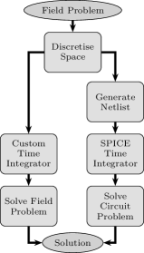
In this paper, we present a method to automatically generate netlists representing general 3D ET and EM coupled field problems. In our approach, neighbouring cells in the primal grid interact via the parallel connection of circuit elements as illustrated in Figure 1a. Thus, the size of the resulting circuit depends on the geometrical size of the problem and the fineness of the discretisation grid. This allows to use any available circuit simulator. Hence, the need for a dedicated field solver with a custom time integrator is alleviated. To accomplish this, we employ the FIT for discretising the relevant continuous field equations. In contrast to Yee’s finite difference scheme employed by Ramachandran et al [33], FIT is a structure-preserving discretisation strategy which does not require further approximations in dealing with the field and material quantities. Moreover, the concept of integral quantities used in the FIT translates naturally into the framework of circuit descriptions. In this manner, we obtain an exact grid representation of the field equations that we map transparently into circuit stamps. In these stamps, which are associated only with primal edges, lumped elements are directly taken from the entries of the material matrices. These entries are properly integrated constitutive parameters. In Figure 1b, we summarise our approach. In addition to previous work on ET problems [45], we also present a more elaborated description and implementation of boundary conditions and excitations. We also point out that the methodology presented herein allows for straightforward field-circuit coupling and is especially useful for an accurate representation of small devices in a larger circuit. In order to simulate wave propagation problems on a finite computational domain by means of circuit simulation, we present absorbing boundary conditions (ABCs) [46, 47].
The outline of this paper is as follows. In Section 3, we provide the required basics of the FIT. The fundamentals of the MNA are summarised in Section 4. Then, the main part of the paper starts with the circuit representation of ET field problems in Section 5. How to extract circuit stamps for EM field problems is presented in Section 6. Finally, we show numerical examples in Section 7 and conclude the paper in Section 8.
2 Continuous Thermal and Electromagnetic Formulations
Let us consider a domain with boundary and characterised by the constitutive parameters , where is the electric permittivity, is the magnetic reluctivity and is the electric conductivity. For every facet , every volume and with impressed electric sources , the EM field in is given by Maxwell’s equations
| (1a) | ||||
| (1b) | ||||
| (1c) | ||||
| (1d) | ||||
We call henceforth (1) the E-H formulation for conciseness. Above, and are the electric and magnetic flux density, respectively, is the electric conduction current and is the electric charge density. To guarantee the uniqueness of the solution, Maxwell’s equations are supplemented with the constitutive relations, viz.
with suitable initial and boundary conditions (BCs) on .
We also deem it convenient to obtain Maxwell’s equations involving the auxiliary magnetic vector potential . To this end, we recall that and , with an auxiliary scalar potential , a gauging material parameter and an arbitrary scalar gauging function . Substitution of these definitions in (1) and applying Stokes’ theorem yields
| (2a) | ||||
| (2b) | ||||
| (2c) | ||||
| (2d) | ||||
which we refer to as the E-A formulation.
Whenever conducting materials are involved, electric currents result in Joule losses that enter as source term into the heat equation which is given by
| (3) |
where is the volumetric heat capacity, is the temperature, is the thermal conductivity and represent any impressed thermal flux density. In general, when thermal effects are considered, all constitutive parameters are also a function of the temperature. To perform circuit extraction, we shall consider the above ET and EM formulations separately as described in Sections 5 and 6, respectively.
3 Discretising the Thermal and Electromagnetic Formulations
We discretise the domain into a pair of orthogonal grids given by the primal grid and its dual . The grid consists of primal points , primal edges (lines) , primal facets (areas) , and primal volumes . Similarly, the grid consists of dual points , dual edges , dual facets , and dual volumes . The grids and are dual to each other in the sense that a primal edge intersects a dual facet and a primal point is located inside a dual volume and vice versa. For a regular hexahedral grid, the grid staggering is depicted in Figure 2. Due to this duality, the number of primal and dual grid objects fulfils
As mentioned above, we write for the -th edge of the primal grid and we emphasise the duality of edges and facets by using the same index. Thus, is the dual facet corresponding to the primal edge and is the dual edge corresponding to the primal facet . Let us further introduce a short (index) notation for geometric objects. If or are used as an index, we simply write instead. Whether refers to an edge or a facet should become clear from the context. For the dual objects, we use instead of or . The notation for points and volumes and their duals is done accordingly. In Table 1, we summarise this notation.

| Description | Normal | Index |
|---|---|---|
| -th primal point | ||
| -th dual point | ||
| -th primal edge | ||
| -th dual edge | ||
| -th primal facet | ||
| -th dual facet | ||
| -th primal volume | ||
| -th dual volume |
The grid counterparts of the field quantities are allocated to points, edges, facets or volumes and collected in column vectors. Typical examples from electromagnetics (EM) are the discrete electric potentials , fields , currents and charges that are allocated to primal points, edges, facets and volumes, respectively. The number of bows indicates the dimension of the corresponding geometric object. Nevertheless, we typically write instead of for conciseness. Defining all other grid quantities accordingly, their allocation used in this paper is shown in Figure 2. Furthermore, if we want to indicate a grid quantity, e.g. an electric field, to be allocated to an edge that is part of the boundary of a facet (), we use the indexed notation . To relate grid quantities on either the primal or dual mesh, topological matrices, corresponding to the continuous topological operators, have to be defined. The incidence between grid points and edges is given by the discrete gradient matrix . For an oriented edge , if is the starting point of the edge, if is the ending point of the edge and if is neither starting nor ending point of the edge (). To express the incidence between grid edges and facets, we use the discrete curl matrix . Given a primal facet and its oriented boundary , if edge is oriented in opposite direction than , if edge is oriented in the same way as and if does not touch (). Finally, the discrete divergence matrix denotes the incidence between grid facets and volumes. For a primal volume and its oriented boundary , the entries of are defined in analogy to those of and . Additionally, we have the dual gradient, curl and divergence matrices , and , respectively, defined accordingly. Useful relations between the topological matrices on the primal and dual grids are given by , and [48].
To relate quantities on the primal grid to quantities on the dual grid and vice versa, material relations are employed. For the problem formulated in Section 2, the following three different kind of relations can be identified:
-
•
Quantities allocated to primal facets must be related to quantities allocated to dual edges.
-
•
Quantities allocated to primal edges must be related to quantities allocated to dual facets.
-
•
Quantities allocated to primal points must be related to quantities allocated to dual volumes.
As representatives for the above listed constitutive relations, we formulate three discrete material laws as
where is the magnetic reluctance matrix mapping the discrete magnetic flux allocated to primal facets to the discrete magnetic field allocated to dual edges, is the electric capacitance matrix mapping the discrete electric field allocated to primal edges to the discrete electric flux density allocated to dual facets, and is the thermal capacitance matrix mapping the time derivative of the grid temperature allocated to primal points to the discrete heat power allocated to dual volumes. For other constitutive parameters, the material matrices are defined following these three cases.
Having established the grid constructs and and the corresponding topological and material matrices, the E-H formulation (1) of Maxwell’s equations upon such a grid pair can be written as [5]
| (4e) | ||||
| (4o) | ||||
| (4s) | ||||
| (4w) | ||||
where is the electric conductance matrix, is the discrete magnetic flux density, is the discrete impressed electric current density and is the discrete electric charge. Similarly, with the discrete vector potential , the discrete E-A formulation is given by
| (5e) | ||||
| (5o) | ||||
together with the discrete form of the gauging
| (6) |
where is the discrete counterpart of the gauging function and is a gauging matrix. Since maps from quantities on primal edges to dual facets, it shares properties with the material matrices (e.g. ) and thus can be interpreted as a material matrix with a material value equal to .
Casting also the heat equation (3) into a spatially discrete form, we obtain
where is the thermal conductance matrix and is the discrete vector of the Joule losses. For details on the computation of , we refer the reader to the work by Casper et al [45]. The impressed thermal fluxes are given by their discrete representative .
3.1 Finite Integration Technique and its Relation to Other Discretisation Schemes
For the circuit extraction from 3D field models as presented in this paper, we require diagonal, symmetric and positive definite material matrices. To fulfil this requirement, we choose to use the FIT and assume the material to coincide with the primal grid cells, see Figure 2. While the FIT has also been formulated for anisotropic materials [49], diagonal material matrices are obtained only in the isotropic case or in the case when the principal axes of anisotropy coincide with the coordinate axes. Then, the entries of the different material matrices are given by
where , , , , and are obtained by a suitable averaging scheme [48, 50] and represents the measure (i.e. area, length or volume) of the corresponding geometrical object.
When using the FIT as the discretisation scheme with a canonical numbering of the grid nodes, the curl and material matrices exhibit the block structure
| (7) |
where , are the grid differential operators for the different coordinate directions. Here, was used as an example whereas an equivalent block structure applies for all other material matrices. Within the theory of the FIT, the discrete quantities , , , that were introduced in Section 3 are defined by means of integration with respect to their corresponding geometrical object, such that
where an analogous definition applies for , , and . Due to the applied integration, one speaks of grid voltages instead of discrete fields, of grid currents (fluxes) instead of discrete current (flux) densities and of grid charges instead of discrete charge densities.
As an alternative to the FIT, equivalent approaches such as the cell method [51] or the FEM can be used as long as the orthogonality and one-to-one relation between primal and dual grid objects is guaranteed. When using FEM, linear basis functions together with an appropriate mass lumping for the material matrices must be used to obtain an equivalent scheme [52].
4 A Primer on Circuit Theory and the Modified Nodal Analysis
In this section, we briefly review some fundamentals about circuit theory and the MNA [15, 53]. Kirchhoff’s current and voltage laws are derived and form the basics for circuit analysis.
Any circuit can be understood as a directed graph consisting of interconnected nodes and branches. Let be one of the nodal potentials in a circuit and one of directed branches. With the incidence matrix linking nodes and branches, the voltage-potential relation is given by
The entries of are defined such that if the branch is directed away from node and if is directed towards . If is neither starting nor ending point of , then . With this definition, the exemplary voltage on the branch directed from to is given by .
For time invariant geometries, the current continuity equation reads
| (8) |
for an arbitrary volume . By considering a volume around an arbitrary circuit node and assuming that capacitive charges are located either fully inside or outside of , the total charge and also the charge’s change rate in is zero. Therefore, (8) becomes
If is composed by a finite number of conductors with cross-sectional areas , Kirchhoff’s current law (KCL) is obtained as
| (9) |
where is the total current through the facet . This relation is also depicted in Figure 3a. To express (9) for all nodes in the circuit (cf. Figure 3b), the incidence matrix can be used such that
| (10) |
where is a vector of all currents allocated to the branches and is a vector of zeros of suitable dimension.


In a circuit, the basic branch elements are conductors, capacitors, inductors as well as voltage and current sources. As these elements are allocated to branches, sets of , , , and branches are defined. Hence, can be arranged into a block matrix with sub-blocks for these elements [53], viz.
A circuit example consisting of a current source, two resistors and two capacitors together with the corresponding block structure of is shown in Figure 3c. A similar subdivision is done for the current and voltage vectors,
With these definitions, the voltages are given by
| (11) |
and (10) becomes
| (12) |
The relation between voltages and currents for the different branches is established by constitutive diagonal matrices that contain the element-wise material parameters. These are the conductance, capacitance, and inductance matrices , and , respectively. Expressing the corresponding source branches by means of the source voltages and source currents , this relation becomes
| (13) |
Combining (11), (12) and (13), we obtain the MNA formulation
| (14) |
Note that in contrast to the standard MNA theory, (14) still requires regularisation, typically done by the introduction of a reference (ground) node.
5 Circuit Representation of Electrothermal Field Problems
In this section, we derive the circuit representation for transient ET field problems. We apply the electroquasistatic (EQS) approximation [54] to Maxwell’s equations given by (1) and consider the coupling with the transient heat equation given by (3). Then, the bi-directionally coupled system in differential form reads
| (15a) | ||||
| (15b) | ||||
with suitable initial and boundary conditions. The coupling is manifested by the Joule heating given by in one way and by the temperature dependent conductivity in the opposite way. Due to the EQS approximation, this formulation does not account for inductive effects but does consider resistive and capacitive effects. For simplicity, we neglect the temperature dependency of the permittivity and of the volumetric heat capacity . Applying FIT upon the ET system of (15), the semi-discrete formulation reads
| (16d) | ||||
| (16h) | ||||
with initial and boundary conditions yet to be applied. Note that the system (16d) requires a regularisation which is typically done by choosing a reference (ground) node , where is one of the entries of .
To generate the netlist for formulation (16), the electric and thermal sub-problems are considered separately. The connection is subsequently established by the Joule losses and the temperature dependent electric conductivity. Next, in Section 5.1 and Section 5.2, the netlist generation for the EQS case and the thermal case is presented, respectively. Temperature dependent materials are discussed in Section 5.3 and finally, the implementation of initial and boundary conditions is described in Section 5.4. This allows us to formulate an algorithm for the ET netlist generation as presented in Section 5.5.
5.1 Electroquasistatic Circuit Representation
Let us now concentrate on the EQS sub-problem given by (15a). Since inductances are neglected in the EQS case, (14) simplifies to
| (17) |
Thus, by inspection of (16d) and (17), we are led to the following equivalences:
-
•
The incidence matrices and coincide with the FIT divergence matrix .
-
•
The capacitance matrix coincides with the FIT capacitance matrix .
-
•
The incidence matrices and coincide with the identity matrix.
-
•
The conductance matrix coincides with the FIT conductance matrix .
-
•
The nodal voltages correspond to the FIT degrees of freedom .
-
•
The source currents are given by the divergence of the impressed currents .
-
•
The source voltages correspond to the Dirichlet potentials , which are related to the reference node .
-
•
These equivalences also prevail themselves in the physical units.
Summarised, the field-circuit relations for EQS read
| (18a) | ||||
| (18b) | ||||
| (18c) | ||||
| (18d) | ||||
| (18h) | ||||
| (18i) | ||||
where is the identity matrix of corresponding size and represents the potentials on the Dirichlet boundary nodes. To find the circuit stamp of each edge in the grid upon which (16d) holds, we employ the equivalences of (18) from which the circuit topology is derived. From (18a), conductors and capacitors are placed along the branches of the circuit. According to (18b), the values of the conductors and capacitors are directly taken from the corresponding FIT material matrices.

Current and voltage sources are connected between a circuit node and ground as indicated by (18c). Furthermore, (18d) shows that the circuit’s nodal potentials are equal to the potentials at the grid points. According to (18h), the current sources in the circuit represent the divergence of the FIT impressed currents. Finally, if Dirichlet BCs are imposed, voltage sources in the circuit represent FIT Dirichlet potentials as given by (18i). We further discuss BCs in Section 5.4. To summarise, if we consider an exemplary grid edge , we obtain a representative EQS circuit stamp as shown in Figure 4. Note that the temperature dependence of the materials is neglected for now and will be discussed in Section 5.3
5.2 Thermal Circuit Representation
In this section, we describe the circuit representation of the sub-problem described by (15b). By comparing (16h) to (16d), we observe a slightly different equation structure. Thermal capacities are not subject to spatial differences and thus do not link to neighbouring nodes. Instead, a thermal capacitance influences the change rate of the absolute temperature of a node. Thus, thermal capacitances are placed on branches connecting the nodes to a reference node at zero temperature. This reference node is an additional non-physical node that is introduced to obtain a consistent circuit representation. In the literature, this approach is also referred to as the Cauer model representing a discretised image of the heat flow [55, 56]. An equivalent approach is the Foster model, in which the capacitances are placed between the circuit nodes and the parameters are adjusted accordingly. In the Foster model, the heat propagation is instantaneous and does not account for the fact that an object requires some delay before changing its temperature.
The MNA formulation of (14) must be extended by this additional reference ground node such that
| (19) |
with
where is a column vector of ones of appropriate size and . With these definitions, the equivalences between the MNA formulation of (19) and the thermal formulation of (16h) are readily obtained as
| (20a) | ||||
| (20b) | ||||
| (20c) | ||||
| (20d) | ||||
| (20h) | ||||
| (20i) | ||||
where represents the temperatures at Dirichlet boundary nodes. To derive the circuit stamp of each edge in the grid upon which (16h) holds, we employ the equivalences in (20) from which the circuit topology is derived. From (20a), we infer that capacitances, voltage and current sources are directly connected between a circuit node and the thermal ground. As in the EQS case, conductors connect two neighbouring nodes in the grid as seen from (20b). The values of the conductors and capacitors are taken directly from the matrices and according to (20c). In this manner, the nodal potentials represent the sought temperatures as seen from (20d). The current source is the sum of Joule losses, in fact represented by CCCSs, and the impressed heat flux according to (20h). Finally, if Dirichlet BCs are given, these are modelled by voltage sources in the circuit as stated in (20i). We further comment on BCs in Section 5.4. To summarise, if we consider an exemplary grid edge , we obtain a representative thermal circuit stamp as shown in Figure 5a. Note that the temperature dependence of the materials is neglected until now and will be discussed in Section 5.3.

To further highlight the equivalences between electric and thermal circuits, we would like to briefly comment on this. Many quantities in electrical circuits can find their equivalent in thermal circuits. For example, electric potentials are equivalent to temperatures while electric currents are equivalent to heat fluxes. In Table 2, some of these equivalences are summarised.
| Electrical Circuit | Thermal Circuit |
|---|---|
| electric potential () | temperature () |
| electric voltage () | temperature difference () |
| electric current () | thermal heat flux () |
| electric charge () | thermal energy () |
| electric conductor () | thermal conductor () |
| electric capacitance () | thermal capacitance () |
5.3 Temperature Dependent Materials
Most materials exhibit temperature dependent behaviour. For the kind of considered materials, the temperature mainly influences the electric and thermal conductivity of the involved materials. In this section, we describe an approach to account for a temperature-dependent electric conductivity when generating the corresponding SPICE netlist. Nevertheless, the presented approach can be applied accordingly to other material’s temperature dependencies as well, e.g. the thermal capacity.
Since the SPICE elements that represent the electric conductivities are conductors placed in circuit branches (cf. Section 5.1), we first need to define the temperature of a branch . To this end, we take the average temperature of the nodes interconnected by the branch . Assuming that the temperature dependence of the electric conductivity is known, the temperature-dependent electric conductance of branch is given by
| (21) |
We implement (21) by means of behavioural sources in the SPICE language.
5.4 Initial Conditions and Boundary Conditions
When a coupled problem of more than one transient differential equation is considered, each sub-problem requires its own initial conditions and BCs. Therefore, we impose these conditions on the EQS and thermal sub-problems separately. However, certain equivalences allow to follow the same procedure for both sub-problems. For any kind of transient problem, initial conditions are required. As every SPICE dialect supports specifying initial conditions, these can be directly imposed by the corresponding syntax in the netlist. For electric problems, different types of BCs are of interest. In low-frequency problems as the EQS case, Dirichlet or Neumann conditions are typically used. Dirichlet BCs conditions correspond to a fixed potential enforced at the boundary, while Neumann conditions prescribe the electric current through the boundary. Similarly, in thermal problems, Dirichlet BCs correspond to a prescribed temperature at the boundary, while Neumann BCs prescribe thermal fluxes through the boundary. Additionally, thermal problems commonly also involve Robin BCs that describe convective and radiative boundaries.
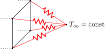
Dirichlet BCs are represented in the circuit by voltage sources between the ground node and the Dirichlet nodes. Homogeneous Neumann conditions are automatically fulfilled since no edge or branch leaves the domain. For simplicity, we do not consider inhomogeneous Neumann conditions in this paper. A Robin BC can be understood as a conduction between a boundary node and an external node representing the fixed ambient temperature . Therefore, Robin BCs are represented in the circuit by conductors connected between the boundary nodes and as shown in Figure 5b. We collect the relevant BCs in Table 3.
| Boundary Condition | Implementation |
|---|---|
| Dirichlet | lumped voltage sources |
| hom. Neumann | no edges leaving the circuit |
| Robin | additional non-physical ground |
5.5 Electrothermal Netlist Generation
To finalise this section, we formulate Algorithm 1 to automatically generate ET SPICE netlists. For every grid edge that connects grid points and , where , the thermal conductance, electric capacitance and the temperature dependent electric conductance (cf. Section 5.3) are written to the netlist connecting nodes and of the circuit (lines 2–4). Due to the possible non-linearity of the electric conductivity (cf. Section 5.3), a behavioural source is used, where is the voltage between node and . Initial conditions (ic) for the electric part can be included using the corresponding syntax for the capacitors. Here, we use exemplary zero initial conditions. Additionally, for every grid point , the thermal capacitance and the current controlled current source (CCCS) representing the Joule losses are added to the netlist connecting node and the ground node (gnd) of the circuit (lines 5 and 6)111For a straight-forward implementation, we use behavioural sources instead of CCCSs. Initial conditions (ic) for the thermal part are specified by pre-charging the thermal capacitors with the initial temperature . To specify a CCCS in the SPICE language, a behavioural source is used. If is specified as an electric (thermal) Dirichlet node, an additional voltage source connecting node and the ground node of the circuit is inserted (lines 9–14). Furthermore, if an impressed current (heat flux) flows out of , an additional current source is added to the netlist connecting node and the ground node of the circuit (lines 15–20).
6 Circuit Representation of Electromagnetic Field Problems
In this section, we neglect thermal effects and describe the circuit representation of general 3D EM field problems as given by (1)–(2). However, the thermo-EM coupling can be established analogously. First, in Section 6.1, we introduce an auxiliary set notion to collect specific edges and facets of the grid. In Section 6.2, the E-H formulation (4) and the E-A formulation (5)–(6) of the Maxwell grid equations (MGEs) are transparently mapped into an electric circuit that fully describes the problem at hand. Finally, in Section 6.3, we extend our analysis in order to realise ABCs as circuit stamps. These are typically needed to limit the computational domain while minimising unphysical reflections caused by the domain truncation.
6.1 Auxiliary Sets of Edges and Facets
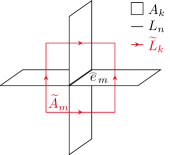
In the following sections, we will take sums over specific edges or facets of the grid. Since the edges and facets in the neighbourhood of a specific edge are of interest, we introduce sets containing collections of these edges and facets and label them with the superscript m. Let be the set of all facets in which is embedded. For a regular hexahedral grid, these facets are shown in Figure 6. All edges that are embedded in the facets contained in are collected in the set , where this definition also implies . We denote by the resulting set after extracting the very edge from , that is . Additionally, we denote the edges that are embedded in facet by the sets and , respectively. The definitions of the sets , , and are visualised in Figure 6 for the case of a regular hexahedral grid. For such a grid, , , and contain , , and edges, respectively. In Section 6.2.2, an additional tree and cotree splitting is introduced. Thereby, edges can either belong to the tree or the cotree. This motivates the introduction of the subscripts t and c to denote tree and cotree, respectively. The additional auxiliary sets that are used due to this splitting are denoted by , , and . Lastly, the dual edges that are embedded in the dual facet are collected in the set .


6.2 Circuit Representation of the Maxwell Grid Equations
In this section, circuit representations of the MGEs given by (4)–(6) are derived. First, we start with the E-H formulation of (4) to find a corresponding circuit description which is presented in Section 6.2.1. Subsequently, in Section 6.2.2 a circuit description based on the E-A formulation of (5)–(6) is presented. For this formulation, a tree-cotree decomposition is used.
6.2.1 Circuit Representation Based on the E-H Formulation
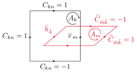
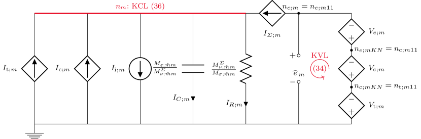
A first electric circuit representing the MGEs is realised from the E-H formulation of (4). The goal is to find an expression for the electric voltage on one primal edge such that a circuit stamp for each edge is obtained. Let be the edge of interest with its corresponding dual facet . We collect all relevant quantities on the grid objects in the neighbourhood of by using the notation introduced in Section 6.1. To find the voltage on , let us consider the pair of interlocked facets and as illustrated in Figure 8a. For this part of the grid, it suffices to consider only the -th row of (4e) and the -th row of (4o) giving
| (22e) | ||||
| (22o) | ||||
From (22e), the magnetic grid voltage allocated at edge (which happens to be also embedded in facet ) reads
| (23) |
By inserting (23) in (22o) for all , the voltage on edge is implicitly given by
Since is contained in , we can extract the contribution of from the sum on the left hand side such that
| (24) |
We further define
| (25a) | ||||
| (25g) | ||||
Thanks to the properties , and , we have that and thus their product equals to unity. However, the product can be either or as illustrated by Figure 8a. Thus, we write (24) with the help of (25g) compactly as
| (26) |
Equation (26) is the Kirchhoff’s current law (KCL) associated with the primal edge with representing the voltage drop along the edge. In fact, according to the definitions of the field quantities in (26), it is easy to realise that
-
•
has unit of voltage (),
-
•
has unit of current (),
-
•
is positive and has unit of capacitance (),
-
•
is positive and has unit of conductance (),
-
•
is positive and has unit of reluctance (),
-
•
has unit of current ().
Thus, by using voltage controlled current sources (VCCSs) to model accounting for the contributions from neighbouring edges, we can directly represent (26) with the circuit stamp depicted in Figure 7, which preserves the voltage drop between the terminals of . There are as many of these stamps as primal edges in , and all of them interact via VCCSs. The concatenation of these elementary stamps constitutes the electric circuit representing the electromagnetic problem at hand.

In Algorithm 2, the steps to generate the netlist representing the EM circuit for the entire grid are listed. A circuit stamp, as shown in Figure 7, needs to be created for every edge in the grid which is realised by a loop in the code. In each iteration, a resistor, inductor and capacitor with the values taken from the material matrices is added (lines 2–4). If an impressed current source shall be placed on , an independent current source with a predefined value is used (lines 5–7). Finally, an inner double loop is required to insert the controlled current sources that model the influence of the edges in the neighbourhood. For this purpose, we choose to insert CCCSs 222Due to the integral term in the expression for , a direct translation into VCCSs is not possible. Instead, behavioural sources or CCCSs can be used. being controlled by the current with a gain of (lines 8–12). By abuse of notation, we denote the controlling device by .
We remark that a similar analysis on (4) in which magnetic conductivities and sources are considered instead of electric ones can be done333Although magnetic carriers have not been observed in nature, there may be situations in which one can profit from the inclusion of an equivalent magnetic conductivity in Maxwell’s equations [57, 58].. This approach would lead to a circuit stamp that is dual to the one in Figure 7. Namely, in this dual stamp, the Kirchhoff’s voltage law (KVL) is guaranteed for each dual edge and represents the electric current in the circuit. Furthermore, the resulting lumped elements, stemming from the material matrices, are placed in series with the discrete impressed magnetic current that plays the role of an independent voltage source exciting the circuit. The interaction between the dual stamps is mediated via current controlled voltage sources (CCVSs). In the general case, when both electric and magnetic sources are present, the electric circuit will consist of both the primal and dual stamps, which interact via CCCSs and VCVSs, accordingly.
6.2.2 Circuit Representation Based on the E-A Formulation
In this section, we describe a circuit representation based on the E-A formulation of (5)–(6). To guarantee uniqueness of the solution, the magnetic potential is gauged by means of a tree-cotree decomposition [59]. Therefore, although the inferred circuit stamps are gauge dependent, the solution obtained for is unique. We start by considering one primal facet (cf. Figure 8a). For this facet, it suffices to consider the -th row of (5e) and the -th row of (5o) such that the E-A formulation of the MGEs for a generic edge reads
| (27e) | ||||
| (27o) | ||||
As in Section 6.2.1, we aim at finding a unique circuit representation of edge . We start by observing that the system matrix of (5) is singular444Note that this is also true for the corresponding continuous operator.. This singularity manifests itself in the non-uniqueness of . In fact, only the curl of is uniquely defined. As a remedy, we must explicitly impose the gauging (6) upon (5). To this end, let us assume that we have constructed a suitable tree and a cotree out of the primal grid , as exemplified in Figure 9. Then, we symbolically introduce the orthogonal permutation matrix to partition into its tree and cotree components with and entries, respectively.
Symbolically, this reads
| (28) |
Similarly, we also divide and into their tree and cotree components by applying the matrix accordingly, viz.
| (29) |
The identities of (28) and (29) together with the orthogonality property of enable us to rewrite the gauging of (6) as
| (30) |
Additionally, since is a square and invertible matrix555These two properties come from two facts: the squareness is a consequence of removing the row associated with the ground node required in circuit analysis. The invertibility is due to removing the non-null kernel space of the matrix by means of the tree-cotree decomposition., we may finally express the tree component as
The column vector , which represents the grid counterpart of the scalar function quantifying the divergence of , is of free choice. Therefore, we conveniently choose impressing the Coulomb gauge [60] to straightforwardly arrive at
| (31) |
The matrix is known as the essential incidence matrix [59] and establishes a direct relation between the tree and cotree components and , respectively666Owing to this property, we identify in the rows of the collection of all fundamental cut-sets associated with the selected tree and cotree. We recall that a fundamental cut-set is a set formed by the union of a single tree edge and the unique set of adjoining cotree edges. In this manner, the fundamental cut-sets are used to express Kirchhoff’s current law in the general form of (31).. By inspection and expansion of (31), we express the -th component of the column vector as
| (32) |
with
and spanning over the nodes in . In this manner, (32) removes the redundancy associated with and guarantees a unique solution of (27).
Let us now get back to the generic primal edge once again. As introduced in Section 6.1, we use specific sets to refer to edges in the tree and cotree denoted by , and , , respectively. Isolating the voltage along edge embedded in facet from (27e), we arrive at
We may then take the sum over all facets (cf. Figure 8b). Then, by splitting into tree and cotree components, we arrive at
| (33) |
where is the number of facets in containing the edge . Note that for a regular hexahedral grid. Let us now introduce the auxiliary definitions
where
which allow to express (33) as
| (34) |
Similarly, we expand the left-hand side of (27o) as
which, upon substitution in (27o) and by splitting into tree and cotree components, yields
| (35) |
where
since . By means of the auxiliary definitions
where
we express (35) as
| (36) |
We observe that (34) and (36) can be interpreted as the KVL and KCL of an arbitrary primal edge provided that and represent the sought voltage and current, respectively. As a matter of fact, we observe that
-
•
has unit of and represents the voltage drop along that is either in the tree or cotree set.
-
•
has unit of Weber () and represents the current along . If , this current is a degree of freedom. Otherwise, it is modelled by a CCCS as stated in (32). For compact notation, we label this CCCS as , where .
-
•
has unit of and is expected to be positive since for all materials. This term scales the displacement, conduction and impressed current as seen in (35).
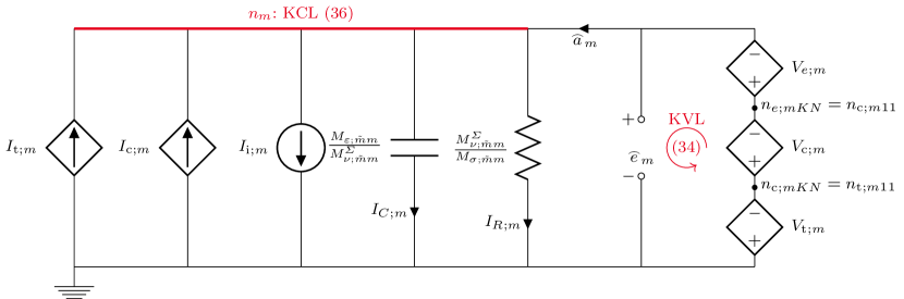
With these observations, we may depict (33) and (35) by means of the circuit stamps of Figure 10a and Figure 10b for a cotree and tree edge, respectively. As we can see therein, is regarded as the electric current along the primal edge , while the voltage drop between its terminals is established by the VCVS and the CCVSs and that mediate the interaction with neighbouring edges. When the edge belongs to the tree , then the current is modelled by the CCCS as demanded by (32). Otherwise, for cotree edges, is a degree of freedom. The current is then split into several branches where a resistance, capacitance, the impressed current source, and CCCSs are connected. The concatenation of these fundamental stamps forms the electric circuit representing the magnetic vector potential formulation of the electromagnetic problem.
In Algorithm 3, we show the pseudocode to generate the netlist of the circuit stamps depicted in Figures 10a and 10b. The iteration over all edges in the grid is done in the outermost loop. In each iteration, one resistor and capacitor connecting the node to ground (gnd) must be added to the netlist (lines 2 and 3). If an impressed current is present at , an independent current source with value is added between and gnd (lines 4–6). For every tree edge, the currents from the cotree edges in the neighbourhood are modelled by a parallel connection of CCCSs between and (lines 7–11). Using a double loop, the inductive currents and from the tree and cotree branches, respectively, are added as a parallel connection of CCCSs between and gnd (lines 12–19). The controlling current is given by the current through device FIc and the gain is . Finally, the voltages , and are added as a series connection between and gnd with intermediate nodes indexed by , and (lines 20–30). For the voltage , the voltage between node n and gnd controls a VCVS with a gain of On the other hand, the voltages and are added as behavioural sources using DDT as the SPICE syntax for time derivatives and a gain of . Note that for a cotree edge, the node coincides with the node .
We remark that a similar analysis on (1) by considering only magnetic conductivities and sources instead of electric ones is also possible. Thus, with the auxiliary electric potential and , where is an arbitrary gauging function, circuit stamps which are dual to those shown in Figure 10a and Figure 10b can be found. In these dual stamps, represents an electric current while , namely the grid counterpart of , would be regarded as a voltage drop. Finally, if both electric and magnetic sources were present, then the entire circuit would consist of the aggregate of interacting primal and dual stamps.
6.3 Absorbing Boundary Conditions
In many electromagnetic field simulation set-ups, the computational domain must be bounded. To simulate free wave propagation, one must impose according conditions for the fields at the boundaries of the domain. These conditions are known as ABCs [46] and aim at minimising (ideally cancelling) unphysical incoming reflections. At the boundary of the domain, a distinction is made between normal and tangential components and between longitudinal and transverse derivatives777In this regard, the longitudinal (transverse) derivative coincides with the normal (tangent) derivative at the boundary..
For starters, let , and denote the longitudinal, transversal and temporal derivative operators, respectively. Furthermore, within the context of this analysis, we define . We start the realisation of circuit stamps for ABCs by considering the time-domain wave equation for the electric field in a homogeneous and isotropic medium888Although we restrict ourselves to homogeneous and isotropic media, the analysis can also be extended to more general cases., viz.
| (37) |
Equation (37) can be expanded in terms of the so-called travelling wave operators as
| (38) |
Above, we observe that in an arbitrary point in space, the field can in general be considered as the superposition of an inward and outward travelling wave and , respectively, viz.
which upon substitution in (38) straightforwardly leads to the following set of travelling wave equations,
inasmuch as both wave components are linearly independent. Owing to their definition, the wave components satisfy independently and simultaneously the following999This property can be easily visualised if we consider, for a moment, one-dimensional wave propagation along the -axis. In this circumstance, we have that and representing backward and forward travelling waves at speed with an arbitrary function.,
| (39) |
which tells us explicitly that the outward (inward) travelling wave operator cancels out the inward (outward) travelling wave at any point of interest.
Now, let us get back to (38) to further expand the operators therein to obtain
| (40) |
As we can see, the above wave operators entail the calculation of the inverse of , which generally translates into a global integral operator [61]. In principle, the expansion of this integral operator around the observation point yields the exact explicit representation of the travelling wave operators in (40). However, this approach is contrary to the idea of realising simple and efficient ABCs for circuit simulations.
As a remedy, we may expand as in a Taylor series to yield
| (41) |
The above equation holds for any component of . Furthermore, if the field propagates in free space, we may assume that the operation is negligible in the neighbourhood of an observation point within the spherical wavefront. Hence, we may rewrite (41) in terms of simplified inward and outward travelling wave propagators as
| (42) |
since the general expression of in (42) admits the superposition of inward and outward travelling waves and . Then, to minimise unwanted incoming reflections at a certain boundary given by , we may impose on the condition
| (43) |
in agreement with (39). The condition given by (43) is a first-order ABC known as Engquist-Madja condition [46]. It is a local condition because it is evaluated pointwise taking only into account the wave component propagating perpendicularly to the boundary. Thereby, the condition in (43) states that a practical transparent boundary at can be realised if it is guaranteed that the phase-amplitude of the field on the boundary at a certain time is equal to that one the field had at some previous instant at a point . The practical relevance of (43) comes from its simplicity.
Let us now interpret (43) within the context of the Maxwell grid equations in order to realise circuit stamps associated with the ABCs of (43). To this end, let us consider the grid wave equation for the electric grid voltage , which for time-independent constitutive parameters and non-conducting source-free regions can be obtained from the grid curl equations of (4), viz.
With the structure of the matrices , and given by (7) and the subdivision , the expression
| (44) |
for the component is obtained. Similar expressions can be also obtained for the other two components and .
The grid counterpart of the ABC in (43) is obtained from (44) by extracting the grid wave equation associated with a generic primal edge oriented along the -direction. This yields
| (45) |
with and spanning over the corresponding primal and dual edges oriented along the indicated directions. We make the following observations upon the above grid wave equation.
-
•
Two main grid wave components contribute to the time variation of along . The first of these grid wave components propagates along the -direction and stems from the spatial variation of along this direction as stated by the grid derivatives in . The second one propagates along the -direction and stems from the spatial variation of along this direction as stated by .
-
•
Two secondary grid wave components contribute to the time variation of along . The first one propagates along the -direction and stems from the spatial variation of along the -direction as stated by . The second one propagates along the -direction and stems from the spatial variation of along the -direction as stated by .
-
•
Owing to both the structure of (45) and the grid-like embedding where the propagation takes place, we may apply superposition to treat each propagation direction separately. Therefore, each grid wave component satisfies its own one-dimensional grid wave equation.

We construct the grid counterpart of (43) by adhering to the same principle that led to it. Namely, we take only into account grid wave propagation perpendicular to the boundary of interest. Thereby, let us assume that our boundary is located for example at . Thus, by invoking the superposition principle, we may write the grid wave equation associated with the component that propagates along the -direction as
| (46) |
where we have used the labels (z) and (x) to explicitly indicate directions of propagation. By considering that for sufficiently well-refined grids and we may expect to not vary significantly for the two relevant facets (cf. Figure 11), we may define an average value that enables us to write the leftmost term on the left-hand side of (46) as
with a similar result for the rightmost term on the left-hand side of (46). Thus, together with the property , we may proceed to write (46) as
Above, the term is the grid counterpart of the continuous operator in the wave equation of (37). Analogously, we may assume that in the vicinity of at the boundary , the wavefront of the impinging grid wave is plane. Therefore, we may neglect transverse variations and we arrive at

We observe that is formally the second-order grid derivative of the scalar field along the -direction. This directly leads us to the grid counterpart of (37) in the vicinity of , viz.
Again, this equation can be factorised in terms of grid wave propagators similar to (42) to yield the grid version of (43), viz.
| (47) |
which can be easily extended to other field components and to other boundary orientations. It also states that the grid wave impinging perpendicularly to the boundary at the edge propagates at a speed . A similar result can be obtained if we had used the grid wave equation of the magnetic field . Having said this, we can think of the space between edge and , namely the preceding -edge in -direction, as a homogeneous transmission line with characteristic impedance
and length , see Figure 12. The voltage that excites the line is given by the voltage on edge , namely . Therefore, if one wants to implement the ABC at edge , an impedance must be assigned to . A subsequent circuit extraction can be carried out by implementing either Algorithm 2 or 3.
7 Numerical Examples
In this section, the presented methodology to generate electric circuit stamps representing 3D field problems is applied to several representative numerical examples. In Section 7.1, we use our netlist extraction method as described in Section 5 on an ET problem. The considered ET problem is a 3D field problem corresponding to the series connection of a capacitor and a resistor. While applying an external voltage, the transient heating due to the resulting current is simulated using SPICE and then compared to a field solver reference solution. Additionally, a circuit representation for the ET field problem of a microelectronic chip package is obtained and used for circuit simulation. In Section 7.2, we apply our method of circuit extraction for EM field problems as described in Section 6 to compute the resonant frequencies of a rectangular cavity with perfect electric conducting (PEC) boundaries. This example is quite illustrative and easy to implement because of the required BCs on the cavity walls. It simply suffices not to print the circuit stamp associated with those edges on the wall, meaning that the associated stamps are short-circuited. Furthermore, the availability of an analytic formula for the resonant frequencies permits a direct error assessment. Finally, in Section 7.3, the implementation of ABCs as discussed in Section 6.3 is carried out to investigate reflections at the end of a rectangular coaxial waveguide. For all presented examples, the Matlab® code to generate the corresponding netlists from the discretised 3D field problem is openly available [62].
7.1 Electrothermal Circuit Validation
To validate our netlist extraction method on an ET problem, we consider the Joule heating in a 3D field problem represented by a series connection of an electric resistor and a capacitor. The temperature dependence of the electric conductivity is manifested via the temperature coefficient . The relevant configuration is realised by a brick of two different materials as shown in Figure 13. The brick is of dimension , with the resistive part having a length of and the capacitive part having a length of . At and , PEC electrodes are used. In Table 4, all material properties are summarised for a reference temperature of .
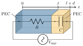
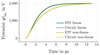
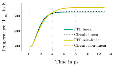
A spatial grid with cells is employed and the field problem is solved by using an in-house implementation of the FIT method with a first-order implicit Euler scheme as time integrator. The simulation time amounts to . For the simulation of the extracted electric circuit, we use the freely available LTspice software101010All circuit simulations in this paper have been done using LTspice in its version 4.22x with default settings.. LTspice uses adaptive refinement in time for which an initial time step of is used. The resulting non-equidistant time axis is refined by a factor of three and then used for the FIT solver. A voltage with is applied at the electrodes as shown in Figure 13. Using this setting, two simulations are run. The first neglects the temperature dependence of the conductivities and thus a linear setting ensues. The second neglects only the temperature dependence of the thermal conductivity but accounts for that of the electric conductivity via the temperature coefficient entailing a non-linear setting. To observe the transient behaviour, we select the resistor-capacitor interface point as observation point and plot the results in Figure 14.
| Symbol | Description | ||
|---|---|---|---|
| electric conductivity | |||
| relative permittivity | |||
| thermal conductivity | |||
| volumetric heat density | |||
| temperature coefficient | – |
For a quantitative error assessment of the solution, we define the measures
| (48) |
where , , and are the potential and temperature solution vectors obtained via circuit and FIT simulation, respectively. To calculate these errors appropriately, the circuit solution is interpolated to the time axis employed by the FIT solution using cubic spline interpolation. We want to remark that the quantities in (48) are not errors in the classical sense since none of the solutions is exact. The computed differences amount to and for the linear case and and for the non-linear case. The remaining error is attributed mainly to the different time integrators.
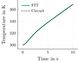
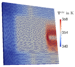
For an industry-relevant example, the proposed method is applied to the 3D microelectronic chip package [45] as shown in Figure 15a. The field problem is discretised as described in Section 3 and Algorithm 1 is used to generate the corresponding netlist. This netlist uses circuit elements to describe a field problem that has been discretised using a grid with nodes. Running a transient analysis on this netlist, an error of and compared to the field simulation is achieved. Figure 15b shows the temperature of the hottest point in the chip package obtained by FIT and circuit simulation. The temperature distribution in the chip package resulting from circuit simulation is shown in Figure 15c. Thus, a good agreement of circuit simulation results for a 3D ET problem is achieved when compared to the corresponding field solver results.
7.2 Electromagnetic Circuit Validation
In this section, we validate the method presented in Section 6 for the circuit representation of EM field problems. To this end, a lossless rectangular resonant cavity with PEC boundaries and outer dimensions of is simulated and its resonant frequencies are computed. The homogeneous material within the cavity is specified by the relative permittivity and the relative permeability for which the resonant frequencies can also be calculated by means of the formula [63]
where is the speed of light and are the indices of the resonant modes and are given by natural numbers including zero. For these resonant frequencies, the longitudinal transverse electric (TE) and transverse magnetic (TM) field components are given by
| (49a) | |||
| (49b) | |||
respectively, where and are the corresponding field amplitudes. For a TE (TM) mode to exist, () must not become zero.
To simulate the excitation of modes within the cavity, we discretise the interior of the cavity using a regular grid of cells in each direction and apply PECs upon all cavity walls. Then, we obtain the resonant frequencies by solving the generalised eigenvalue problem given by
where a resonant frequency is denoted by . Alternatively, we can use appropriate excitations to analyse the resulting field at a set of given frequencies. For example, we can use an electric current source oriented along the positive -direction and attached to the central grid point to excite TM modes. In a similar manner, TE modes are excited by means of a looping electric current source located in the cavity centre. We then solve the discretised problem given by
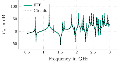
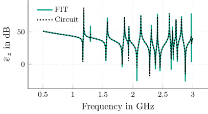
for a set of angular frequencies , where is the current source vector whose entries are all zero except at the corresponding source edges. The frequency axis from to is discretised using points for TM excitation and points for TE excitation. The results are evaluated on one edge for each excitation type. For the TM case, an edge in positive -direction connected to the central grid point is used while for the TE case, an edge in positive -direction connected to the point (5,6,10) is used. In Figure 16, the voltages and along these edges are plotted. From the peaks in the plots, the corresponding resonant frequencies and are identified111111We have used the function findpeaks of Matlab® R2017a to identify the peaks in the plot..
To validate our circuit extraction method for EM problems, we generate the netlist of the resonant cavity according to Algorithm 2 and simulate the resulting circuit in LTspice by performing an AC analysis in the same frequency range as before. We then identify the circuit voltages corresponding to and and plot them also directly in Figure 16 for a comparison. The circuit resonant frequencies and are again identified by means of the peaks and we collect the computed resonant frequencies for the first few modes in Table 5. Note that, according to (49), the TM-mode does not exist for . Additionally, the errors
are presented. For all modes, these errors are much smaller than .
| Mode | (%) | (%) | ||||||
|---|---|---|---|---|---|---|---|---|
| 011 | — | — | — | |||||
| 110/101/012/021 | ||||||||
| 111 | ||||||||
| 121 | ||||||||
| 013 | — | — | — | |||||
| 122 |
7.3 Signal Transmission Using Absorbing Boundary Conditions
In this section, based on the method described in Section 6.3, we present a simple validation example for ABCs in the context of circuit simulation. To this end, let us consider a coaxial transmission line of rectangular cross section oriented along the -direction as depicted in Figure 17. For the simulation of an infinitely long line using a finite computational domain, the implementation of ABCs is required to counteract unwanted incoming reflections. We use an excitation signal at port 1 and simulate its propagation in time until it has reached port 2. Thus, we generate two simulation results in time domain. The first one corresponds to the case when port 2 is terminated with a perfect magnetic wall, that is an open port (). The second one corresponds to the case when port 2 is terminated with the characteristic line impedance (). For both cases, a perfect magnetic conducting (PMC) () at port 1 is applied121212According to image theory, the perfect magnetic wall at port 1 serves as a mirror which reflects uprightly the otherwise backward travelling wave..

The length of the coaxial line is , the width and height of the outer conductor are and of the inner conductor . While the conductors are modelled as PEC, the material between them is vacuum. Due to the expected propagation in -direction, the longitudinal direction requires a finer discretisation compared to the transversal direction. Thus, we choose a grid of cells. According to (47) for such a discretisation grid, the characteristic impedance for the edges connecting the inner and outer conductor along the plane of port 2 should amount to131313Note that in the calculation of , the value employed for is taken directly from the parallel edge just in front of the boundary edge in accordance with the impinging grid wave front speed. . For the given grid, there are eight such edges giving eight parallel conductances such that the total resistance at port 2 equals , which is also the characteristic impedance of the line. To excite the signal at port 1, the edges connecting the inner and outer conductors along the plane of port 1 are impressed with a current such that the total current from inner to outer conductor is
with , which is a Gauss pulse with a maximal frequency141414Confining the excitation to this maximal frequency component, we assure that the TEM mode is the only propagating mode on the line component of . The used constants are given by and by . The simulation time is chosen such that the excited pulse can reach port 2. Having defined the geometry, the excitation and the simulation time, we also generate the corresponding netlist using Algorithm 2.
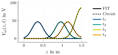
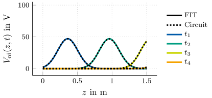
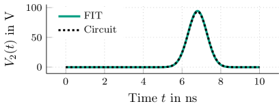
The generated netlist is simulated by means of a transient analysis in LTspice. On the other hand, the Leapfrog scheme is used as a time integrator within the FIT framework to carry out the simulation directly on the 3D grid. In both cases, we use the time axis generated by the adaptive time stepping algorithm provided by LTspice, which satisfies the Courant-Friedrichs-Levy (CFL)-condition being a stability requirement for the explicit Leapfrog scheme [1]. In the following, we compare the voltage between outer and inner conductor and the voltage at port 2. For and , Figure 18 shows at different times computed by means of FIT and circuit simulation. Figure 18a shows the case in which port 2 is terminated by a perfect magnetic boundary (standard homogeneous Neumann) condition while Figure 18b shows the case when a matching impedance according to (47) is applied at port 2. As predicted by the theory in Section 6.3, we observe that the matching impedance at port 2 counteracts incoming reflections effectively. In Figure 19, we show computed by means of FIT and circuit simulation for the two already considered cases. We observe therein that incoming reflections at port 2 result in an undesired overshooting of the voltage. For a quantitative comparison, we define the relative error of between FIT and circuit results as
and obtain and .
8 Conclusion and Future Work
A method for the automatic netlist generation of general 3D ET and EM problems has been presented. The topology of each circuit stamp associated with edges in the regular primal grid has been derived by using FIT for spatial discretisation. Using the MNA, the FIT-discretised ET formulation has been mapped into a circuit that can be solved by any SPICE-like program. It has been shown that initial conditions can be easily prescribed as initial potentials for the lumped capacitances in the SPICE language. Furthermore, the implementation of mixed boundary conditions of Dirichlet, homogeneous Neumann and Robin type has been discussed. We have also shown that temperature dependent material models result in non-linearities in the lumped resistances requiring the implementation of behavioural VCCSs in SPICE.
From the standard E-H formulation and the E-A formulation, we have derived circuit stamps representing general EM problems. In both circuit representations, the integrated electric field models the voltage between the stamp terminals while the integrated magnetic vector potential models the electric current in the E-A formulation. To guarantee uniqueness of the solution in the latter, we have employed Coulomb’s gauge on the magnetic vector potential, that has been implemented by means of a tree-cotree decomposition of the primal discretisation grid. Thereby, the electric current along edges in the cotree are degrees of freedom whereas those along edges in the tree are modelled by CCCSs being controlled by currents in the cotree. For both representations, a dual circuit formulation exists if magnetic sources instead of electrical sources are considered. In the dual case, an auxiliary electric potential would be used instead of the magnetic vector potential. To demonstrate the correctness of our formulations, several numerical examples have been shown for the primal circuits involving electric sources only.
The formulation of inhomogeneous Neumann BCs could be a further extension to the presented approach. Furthermore, the method can also be applied to extract circuits from FEM models. To account for thermal effects in EM problems, the methods for the extraction of ET and EM circuit stamps can be combined to generate a thermo-EM circuit stamp. Methods to account for non-linear material characteristics in the EM case are still to be developed. However, in principle one can follow similar ideas to those presented in the ET case. For large field models, the resulting circuit can become very large. Therefore, to efficiently simulate such circuits, dedicated MOR techniques for circuits can be applied. The first of these techniques is known as the asymptotic waveform evaluation (AWE) proposed by Pillage and Rohrer [64] and extensions developed afterwards. The most prominent ones are the matrix Padé via a Lanczos-type process (MPVL) by Feldmann and Freund [65] and the passive reduced-order interconnect macromodeling algorithm (PRIMA) [66]. More recent approaches are based on the proper orthogonal decomposition [67] and other well-known general MOR techniques.
Acknowledgements
This is a pre-print of an article published in the Journal of Computational Electronics. The final authenticated version is available online at: https://doi.org/10.1007/s10825-019-01368-6. The authors thank Abdul Moiz and Victoria Heinz for their passionate work on implementing the automated electrothermal netlist generation. The work is supported by the European Union within FP7-ICT-2013 in the context of the Nano-electronic COupled Problems Solutions (nanoCOPS) project (grant no. 619166), by the Excellence Initiative of the German Federal and State Governments and the Graduate School of Computational Engineering at Technische Universität Darmstadt.
References
- [1] Kane S. Yee. Numerical solution of initial boundary value problems involving Maxwell’s equations in isotropic media. IEEE Trans. Antenn. Propag., 14(3):302–307, May 1966.
- [2] Allen Taflove. Advances in Computational Electrodynamics: The Finite-Difference Time-Domain-Method. Artech House, Dedham, MA, 1998.
- [3] Thomas Weiland. A discretization method for the solution of Maxwell’s equations for six-component fields. AEÜ, 31:116–120, March 1977.
- [4] Ursula van Rienen and Thomas Weiland. Triangular discretization method for the evaluation of RF-fields in cylindrically symmetric cavities. IEEE Trans. Magn., 21(6):2317–2320, November 1985.
- [5] Thomas Weiland. Time domain electromagnetic field computation with finite difference methods. Int. J. Numer. Model. Electron. Network. Dev. Field, 9(4):295–319, 1996.
- [6] Alain Bossavit. A rationale for “edge-elements” in 3-D fields computations. IEEE Trans. Magn., 24(1):74–79, January 1988.
- [7] Myoung Joon Choi, Kyu-Pyung Hwang, and N. Cangellaris. Direct generation of SPICE compatible passive reduced order models of ground/power planes. In Thomas G. Reynolds, Peter Slota, Mike McShane, and Wayne J. Howell, editors, Proceedings of the 50th Electronic Components & Technology Conference, pages 775–780. IEEE, 2000.
- [8] Yacouba Moumouni and R. Jacob Baker. Concise thermal to electrical parameters extraction of thermoelectric generator for SPICE modeling. In Tom Chen and R. Jacob Baker, editors, IEEE 58th International Midwest Symposium on Circuits and Systems (MWSCAS), pages 1–4. IEEE, 2015.
- [9] Lorenzo Codecasa, Vincenzo d’Alessandro, Alessandro Magnani, and Andrea Irace. Circuit-based electrothermal simulation of power devices by an ultrafast nonlinear MOR approach. IEEE Trans. Power Electron., 31(8):5906–5916, 2016.
- [10] Martin Eller. A Low-Frequency Stable Maxwell Formulation in Frequency Domain and Industrial Applications. Dissertation, Technische Universität Darmstadt, Darmstadt, November 2017.
- [11] Tilmann Wittig, Irina Munteanu, Rolf Schuhmann, and Thomas Weiland. Model order reduction and equivalent circuit extraction for FIT discretized electromagnetic systems. Int. J. Numer. Model. Electron. Network. Dev. Field, 15(5-6):517–533, December 2002.
- [12] L. W. Nagel and D. O. Pederson. Simulation program with integrated circuit emphasis. Technical Report UCB/ERL M382, EECS Department, University of California, Berkeley, April 1973.
- [13] R.S. Vogelsong and C. Brzezinski. Extending SPICE for electro-thermal simulation. In Ray Milano, Marc Hartranft, and Dave Brown, editors, Proceedings of the IEEE 1989 Custom Integrated Circuits Conference, pages 21.4/1–21.4/4, May 1989.
- [14] A. R. Hefner and D. L. Blackburn. Simulating the dynamic electrothermal behavior of power electronic circuits and systems. IEEE Trans. Power Electron., 8(4):376–385, 1993.
- [15] Chung-Wen Ho, Albert E. Ruehli, and Pierce A. Brennan. The modified nodal approach to network analysis. IEEE Trans. Circ. Syst., 22(6):504–509, June 1975.
- [16] Wenquan Sui, Douglas A. Christensen, and Carl H. Durney. Extending the two-dimensional FDTD method to hybrid electromagnetic systems with active and passive lumped elements. IEEE Trans. Microw. Theor. Tech., 40(4):724–730, 1992.
- [17] Yui-Sheng Tsuei, A. C. Cangellaris, and J. L. Prince. Rigorous electromagnetic modeling of chip-to-package (first-level) interconnections. IEEE Trans. Compon., Hybrids, and Manuf. Technol., 16(8):876–883, 1993.
- [18] Melinda Piket-May, Allen Taflove, and John Baron. FD-TD modeling of digital signal propagation in 3-D circuits with passive and active loads. IEEE Trans. Microw. Theor. Tech., 42(8):1514–1523, 1994.
- [19] Vincent A. Thomas, Michael E. Jones, Melinda Piket-May, Allen Taflove, and Evans Harrigan. The use of SPICE lumped circuits as sub-grid models for FDTD analysis. IEEE Microwave and Guided Wave Letters, 4(5):141–143, 1994.
- [20] Karine Guillouard, Man-Fai Wong, V. Fouad Hanna, and Jacques Citerne. A new global finite element analysis of microwave circuits including lumped elements. IEEE Trans. Microw. Theor. Tech., 44(12):2587–2594, 1996.
- [21] Karine Guillouard, Man-Fai Wong, V. Fouad Hanna, and Jacques Citerne. A new global time-domain electromagnetic simulator of microwave circuits including lumped elements based on finite-element method. IEEE Trans. Microw. Theor. Tech., 47(10):2045–2049, 1999.
- [22] Lauri Kettunen. Fields and circuits in computational electromagnetism. IEEE Trans. Magn., 37(5):3393–3396, September 2001.
- [23] Galina Benderskaya, Herbert De Gersem, Thomas Weiland, and Markus Clemens. Transient field-circuit coupled formulation based on the finite integration technique and a mixed circuit formulation. COMPEL, 23(4):968–976, 2004.
- [24] Sebastian Schöps, Herbert De Gersem, and Thomas Weiland. Winding functions in transient magnetoquasistatic field-circuit coupled simulations. COMPEL, 32(6):2063–2083, September 2013.
- [25] Sebastian Schöps. Multiscale Modeling and Multirate Time-Integration of Field/Circuit Coupled Problems. Dissertation, Bergische Universität Wuppertal & Katholieke Universiteit Leuven, Düsseldorf, May 2011. VDI Verlag. Fortschritt-Berichte VDI, Reihe 21.
- [26] Martin Witting. Simulation elektrischer Netzwerke unter Berücksichtigung ihrer elektromagnetischen Umgebung. Dissertation, Technische Universität Darmstadt, Darmstadt, 1997.
- [27] Albert E. Ruehli. Equivalent circuit models for three-dimensional multiconductor systems. IEEE Trans. Microw. Theor. Tech., 22(3):216–221, 1974.
- [28] Albert E. Ruehli, Giulio Antonini, and Lijun Jiang. The Partial Element Equivalent Circuit Method for Electro-Magnetic and Circuit Problems. Wiley and Sons, Hoboken, New Jersey, 2015.
- [29] Robert F. Milsom. Efficient SPICE-compatible electromagnetic model of arbitrarily shaped integrated passive structure. IEEE Trans. Microw. Theor. Tech., 47(7):1033–1044, 1999.
- [30] Giulio Antonini. SPICE equivalent circuits of frequency-domain responses. IEEE Trans. EMC, 45(3):502–512, 2003.
- [31] Peter Russer, Mario Righi, Channabasappa Eswarappa, and Wofgang J. R. Hoefer. Lumped element equivalent circuit parameter extraction of distributed microwave circuits via TLM simulation. In IEEE MTT-S International Microwave Symposium Digest, pages 887–890. IEEE, 1994.
- [32] Myoung Joon Choi and Andreas C. Cangellaris. A quasi three-dimensional distributed electromagnetic model for complex power distribution networks. IEEE Trans. Adv. Packag., 25(1):28–34, 2002.
- [33] Aravind Ramachandran, Anand Ramachandran, and Andreas C. Cangellaris. SPICE-compatible stamps for semi-discrete approximations of Maxwell’s equations. Int. J. Numer. Model. Electron. Network. Dev. Field, 21(4):265–277, 2008.
- [34] A. Chvala, D. Donoval, J. Marek, P. Pribytny, M. Molnar, and M. Mikolasek. Fast 3-D electrothermal device/circuit simulation of power superjunction MOSFET based on SDevice and HSPICE interaction. IEEE Trans. Electron. Dev., 61(4):1116–1122, April 2014.
- [35] S. Wünsche, C. Clauss, P. Schwarz, and F. Winkler. Electro-thermal circuit simulation using simulator coupling. IEEE Trans. Very Large Scale Integr. (VLSI) Syst., 5(3):277–282, September 1997.
- [36] W. van Petegem, B. Geeraerts, W. Sansen, and B. Graindourze. Electrothermal simulation and design of integrated circuits. IEEE J. Solid. State. Circ., 29(2):143–146, February 1994.
- [37] N. Simpson, R. Wrobel, and P.H. Mellor. An accurate mesh-based equivalent circuit approach to thermal modeling. IEEE Trans. Magn., 50(2):269–272, February 2014.
- [38] Luigi Lombardi, Raffaele Raimondo, and Giulio Antonini. Electrothermal formulation of the partial element equivalent circuit method. Int. J. Numer. Model. Electron. Network. Dev. Field, 31(4):e2253, 2018.
- [39] Paul L. Evans, Alberto Castellazzi, and C. Mark Johnson. Automated fast extraction of compact thermal models for power electronic modules. IEEE Trans. Power Electron., 28(10):4791–4802, 2013.
- [40] Mirko Bernardoni, Nicola Delmonte, Diego Chiozzi, and Paolo Cova. Non-linear thermal simulation at system level: Compact modelling and experimental validation. Microelectron. Reliab., 80:223–229, 2018.
- [41] Massimiliano Culpo, Carlo de Falco, Georg Denk, and Steffen Voigtmann. Automatic thermal network extraction and multiscale electro-thermal simulation. In Janne Roos and Luis R. J. Costa, editors, Scientific Computing in Electrical Engineering SCEE 2008, volume 14 of Mathematics in Industry, pages 281–288, Berlin, June 2010. Springer.
- [42] Patrick Wilkerson, Ashok Raman, and Marek Turowski. Fast, automated thermal simulation of three-dimensional integrated circuits. In Koneru Ramakrishna, editor, The Ninth Intersociety Conference on Thermal and Thermomechanical Phenomena in Electronic Systems, ITHERM’04, volume 1, pages 706–713. IEEE, 2004.
- [43] Serap Karagol and Marwan Bikdash. Generation of equivalent-circuit models from simulation data of a thermal system. IEEE Trans. Power Electron., 25(4):820–828, 2010.
- [44] Jia Tzer Hsu and Loc Vu-Quoc. A rational formulation of thermal circuit models for electrothermal simulation. I. finite element method [power electronic systems]. IEEE Trans. Circ. Syst. Fund. Theor. Appl., 43(9):721–732, 1996.
- [45] Thorben Casper, Herbert De Gersem, and Sebastian Schöps. Automatic generation of equivalent electrothermal SPICE netlists from 3D electrothermal field models. In Willem van Driel and Peter Rodgers, editors, 17th International Conference on Thermal, Mechanical and Multi-Physics Simulation and Experiments in Microelectronics and Microsystems (EuroSimE 2016), April 2016.
- [46] Bjorn Engquist and Andrew Majda. Absorbing boundary conditions for the numerical simulation of waves. Mathematics of Computation, 31(139):629–651, 1977.
- [47] Gerrit Mur. Absorbing boundary conditions for the finite-difference approximation of the time-domain electromagnetic-field equations. IEEE Trans. EMC, (4):377–382, 1981.
- [48] Markus Clemens and Thomas Weiland. Discrete electromagnetism with the finite integration technique. PIER, 32:65–87, 2001.
- [49] Holm Krüger, H. Spachmann, and Thomas Weiland. Time domain modeling of gyromagnetic materials using the finite integration technique. IEEE Trans. Magn., 37(5):3269–3272, 2001.
- [50] Thorben Casper, Herbert De Gersem, Renaud Gillon, Tomáš Götthans, Tomáš Kratochvíl, Peter Meuris, and Sebastian Schöps. Electrothermal simulation of bonding wire degradation under uncertain geometries. In Luca Fanucci and Jürgen Teich, editors, Proceedings of the 2016 Design, Automation & Test in Europe Conference & Exhibition (DATE), pages 1297–1302. IEEE, April 2016.
- [51] Piergiorgio Alotto, A. De Cian, and G. Molinari. A time-domain 3-D full-Maxwell solver based on the cell method. IEEE Trans. Magn., 42(4):799–802, April 2006.
- [52] Anders Bondeson, Thomas Rylander, and Pär Ingelström. Computational Electromagnetics. Texts in Applied Mathematics. Springer, 2005.
- [53] Michael Günther, Uwe Feldmann, and E. Jan W. ter Maten. Modelling and Discretization of Circuit Problems, volume 13 of Handbook of Numerical Analysis, pages 523–659. Elsevier BV, Amsterdam, 2005.
- [54] Markus Clemens, Markus Wilke, Galina Benderskaya, Herbert De Gersem, Wigand Koch, and Thomas Weiland. Transient electro-quasistatic adaptive simulation schemes. IEEE Trans. Magn., 40(2):1294–1297, March 2004.
- [55] Y. C. Gerstenmaier, W. Kiffe, and G. Wachutka. Combination of thermal subsystems modeled by rapid circuit transformation. In Bernard Courtois, Márta Rencz, Clemens Lasance, and Vladimir Székely, editors, 13th International Workshop on Thermal Investigations of ICs and Systems (THERMINIC 2007). IEEE, 2007.
- [56] Tamara Bechtold, Evgenii B. Rudnyi, and Jan G. Korvink. Fast Simulation of Electro-Thermal MEMS: Efficient Dynamic Compact Models. MEMS and Microtechnology. Springer Verlag, Heidelberg, Germany, 2006.
- [57] J. R. Wait. Letter to the editor: the “magnetic conductivity” and wave propagation. IEEE Trans. EMC, 34(2):139, May 1992.
- [58] Dmitri E. Kharzeev and Harmen J. Warringa. Chiral magnetic conductivity. Phys. Rev. D, 80(3):034028, August 2009.
- [59] Irina Munteanu. Tree-cotree condensation properties. ICS Newsletter (International Compumag Society), 9:10–14, 2002.
- [60] C.A. Balanis. Advanced Engineering Electromagnetics. CourseSmart Series. Wiley, 2012.
- [61] K. Zhukovsky. Solution of some types of differential equations: Operational calculus and inverse differential operators. The Scientific World Journal, 2014:1–8, 2014.
- [62] Thorben Casper, David Duque, Victoria Heinz, Abdul Moiz, Herbert De Gersem, and Sebastian Schöps. ANTHEM - Automatic Netlist generator for THermo-EM field problems, 2018. https://github.com/tc88/ANTHEM.
- [63] David F. Griffiths. Introduction to Electrodynamics. Prentice-Hall, New Jersey, September 1999.
- [64] Lawrence T. Pillage and Ronald A. Rohrer. Asymptotic waveform evaluation for timing analysis. IEEE Trans. Comput. Aided. Des. Integrated Circ. Syst., 9(4):352–366, 1990.
- [65] Peter Feldmann and Roland W. Freund. Reduced-order modeling of large linear subcircuits via a block Lanczos algorithm. In Bryan T. Preas, Thomas P. Pennino, and Ellen J. Yoffa, editors, Proceedings of the 32nd annual ACM/IEEE Design Automation Conference, pages 474–479. ACM, 1995.
- [66] A. Odabasioglu, M. Celik, and L. T. Pileggi. PRIMA: passive reduced-order interconnect macromodeling algorithm. IEEE Trans. Comput. Aided. Des. Integrated Circ. Syst., 17(8):645–654, 1998.
- [67] Michael Hinze, Martin Kunkel, and Ulrich Matthes. POD model order reduction of electrical networks with semiconductors modeled by the transient drift-diffusion equations. In Michael Günther, Andreas Bartel, Markus Brunk, Sebastian Schöps, and Michael Striebel, editors, Progress in Industrial Mathematics at ECMI 2010, volume 17 of Mathematics in Industry, Berlin, April 2012. Springer.