Spin-Blockade Spectroscopy of Si/SiGe Quantum Dots
Abstract
We implement a technique for measuring the singlet-triplet energy splitting responsible for spin-to-charge conversion in semiconductor quantum dots. This method, which requires fast, single-shot charge measurement, reliably extracts an energy in the limits of both large and small splittings. We perform this technique on an undoped, accumulation-mode Si/SiGe triple-quantum dot and find that the measured splitting varies smoothly as a function of confinement gate biases. Not only does this demonstration prove the value of having an in situ excited-state measurement technique as part of a standard tune-up procedure, it also suggests that in typical Si/SiGe quantum dot devices, spin-blockade can be limited by lateral orbital excitation energy rather than valley splitting.
Qubits based on electrons confined in silicon quantum dots (QDs) benefit from the advantages inherent to many semiconductor platforms: fast control, small form factors, and established fabrication methods. Moreover, mitigation of a dominant decoherence pathway—interactions with non spin-zero nuclei—is possible with isotopic enhancement Ladd and Carroll (2018). These advantages have led to key demonstrations, including extended coherence Muhonen et al. (2014); Eng et al. (2015); Yoneda et al. (2018) as well as fast, accurate control via a number of techniques including tunnel barrier modulation Reed et al. (2016); Martins et al. (2016), electron spin resonance Veldhorst et al. (2014); Muhonen et al. (2015); Fogarty et al. (2017), and induced spin-orbit coupling Kawakami et al. (2016). Recently, one-qubit randomized benchmarking Veldhorst et al. (2014); Zajac et al. (2017); Yang et al. (2018), two-qubit randomized benchmarking Huang et al. (2018), and two-qubit entangling sequences Veldhorst et al. (2015); Zajac et al. (2017); Watson et al. (2018) have been demonstrated with Si-based qubits.
Many quantum dot based qubits rely on the conversion of electron spin states, which preserve quantum information by interacting weakly with their electrical environment, to charge states for control and measurement. In exchange-based schemes, distinct spin states of two interacting electrons (spin-singlets and spin-triplets) are converted into distinguishable charge states utilizing the well-established principles of Pauli spin blockade (SB)Hanson et al. (2007). The robustness of SB relies on the energy separation between the ground-singlet and ground-triplet levels of two electrons occupying the same dot, denoted here as . This energy limits state measurement and preparation fidelities by setting the range over which one can achieve spin-to-charge conversion and the accuracy with which one can initialize a ground state singlet in a system at finite temperature Gamble et al. (2016).
Establishing what sets in Si QDs is crucial for qubit design. While orbital excitation energies are, in principle, easily manipulated by changing confining potentials with gate biases, the maximum attainable is conventionally thought to be limited by valley splitting, the energy splitting between the two lowest-lying quantized states originating from conduction band valleys of bulk, tensily strained silicon Boykin et al. (2004). Two-electron orbital energies are determined by the strength and symmetry of in-plane confinement Melnikov and Leburton (2006); Hanson et al. (2007), whereas valley splittings are determined primarily by the details of out-of-plane electron confinement, a challenge that has inspired many theoretical and engineering efforts Boykin et al. (2004); Sasaki et al. (2009); Zhang et al. (2013); Neyens et al. (2018). Numerous techniques have been used to estimate the magnitude of valley splitting in Si/SiGe quantum dots, including photon-assisted tunneling van der Wiel et al. (2002), cavity coupling Mi et al. (2017), Landau-Zener-Stückelberg interferometry Schoenfield et al. (2017), magnetotransport Neyens et al. (2018), and magnetospectroscopy Lim et al. (2011); Borselli et al. (2011). However, the results of these techniques may not accurately measure as they probe length scales not generally relevant to QD electrons, require the application of additional electromagnetic fields, or use biasing configurations different from nominal operation. These conditions impede a direct translation of the measured energies to qubit performance.
In this Letter, we describe an excited-state spectroscopy technique which directly measures in QDs. The utility of this method lies in its ability to extract both small and large in exactly the bias configuration required to achieve spin-to-charge conversion and without relying on a detailed physical model or the addition of control fields beyond those normally required to operate exchange-only quantum dot qubits. We discuss the requirements placed on our measurement system to perform this technique, which is fundamentally limited by the fidelity of single-shot state discrimination. We then demonstrate this technique on a Si/SiGe double-dot and find to be highly tunable and smoothly varying with bias voltages, suggesting that in this device is limited by orbital confinement energy rather than valley splitting Friesen and Coppersmith (2010); Shi et al. (2011); Yang et al. (2013). Both the establishment of a reliable method for in situ excited-state spectroscopy and the identification of limitations to device performance should be relevant to many QD architectures.
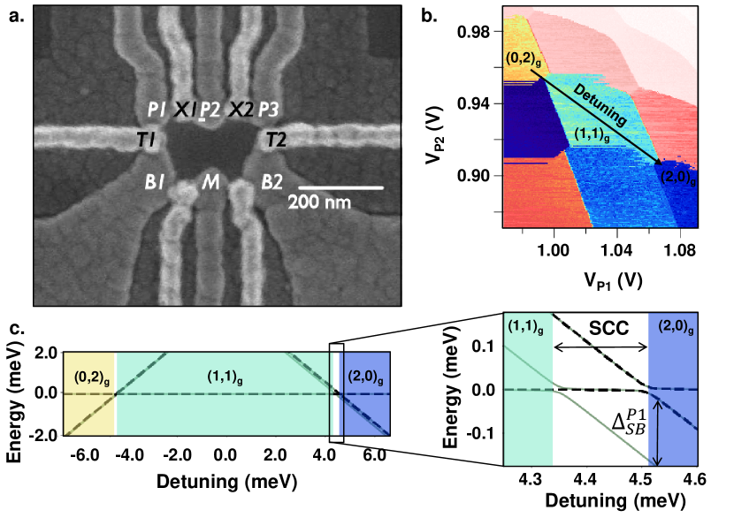
We measure an accumulation-mode, Si/SiGe triple dot (Fig. 1a) which is similar to other devices Lai et al. (2011); Borselli et al. (2015); Zajac et al. (2015); Ward et al. (2016); Studenikin et al. (2018) that have demonstrated both a scalable platform for trapping many electrons Zajac et al. (2016) and universal qubit control Eng et al. (2015); Reed et al. (2016). Building on our previous experience Borselli et al. (2015); Deelman et al. (2016), electrons are confined in a tensile-strained Si quantum well, embedded in a strain-relaxed, undoped SiGe alloy. Lateral confinement is provided by two types of overlapping metal gates: large field gates that prevent the accumulation of electrons in undesirable locations and smaller control gates. Quantum dots are defined under the “plunger” gates labeled , , and and are loaded from electron reservoirs under the “bath” gates and . Tunneling from the baths to the dots is mediated by the “tunnel” gates and , and interdot tunnel coupling is controlled by the “exchange” gates and . Bound electrons capacitively couple to the “measure” dot , with each charge configuration affecting the measured conductance as seen in Fig. 1b. Gate biases provide control of the triple dot through two mechanisms: a linear response in the chemical potentials, which can sensitively calibrate away any residual charge disorder, and an exponential response in tunnel coupling, which allows fast control with large on/off ratios and ultimately facilitates high performance quantum gates.
Spin-to-charge conversion (SCC), by which two-electron spin states are converted into distinct charge states, occurs at biases where two electron number-conserving charge states are nearly degenerate, e.g., bottom-right: (2,0)-(1,1) and top-left: (0,2)-(1,1) of Fig. 1b Kane (1998); Hanson et al. (2007). As dictated by the Pauli exclusion principle, the two-electron spin-symmetric triplet must be antisymmetric in some other degree of freedom. In silicon, this can be provided by valley, orbital excitation, or some hybridization of the two Friesen and Coppersmith (2010). The ground-singlet to ground-triplet energy splitting of two electrons occupying dot , denoted , determines the range of detunings that support SCC, i.e., biases at which the ground-triplet remains in the (1,1) charge state while the ground-singlet occupies a single QD (see Fig.1c). These distinct charge states result in different electrostatic potentials at the measure dot, leading to measurably different conductances at this charge sensor Borselli et al. (2015).
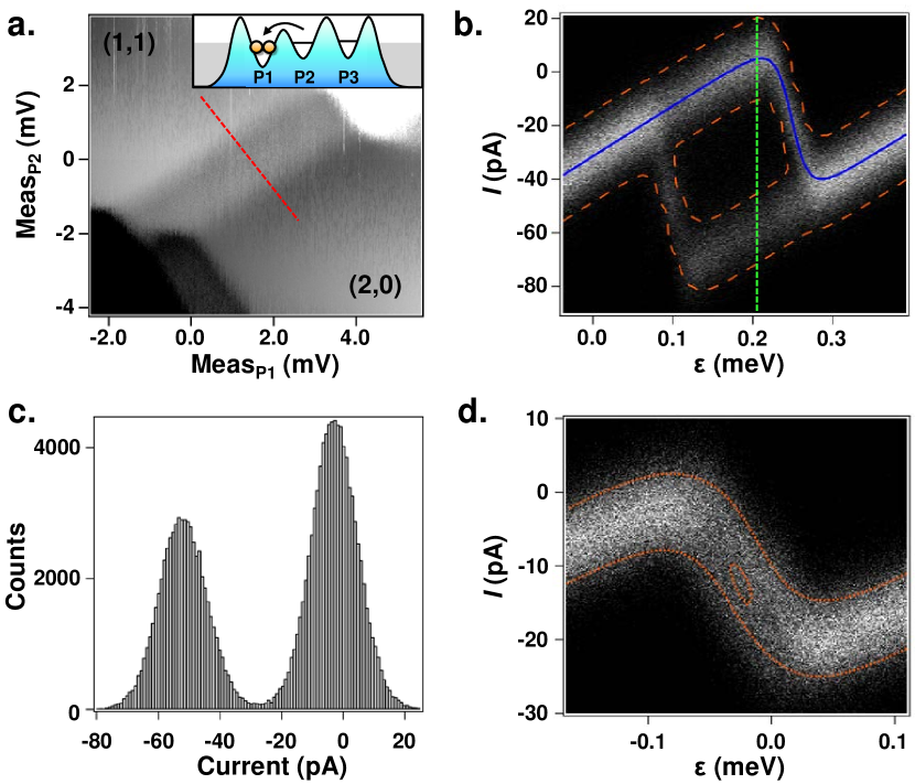
Our technique measures by analyzing single-shot current values as singlet/triplet mixed states are swept adiabatically through detunings that support spin to charge conversion. This involves a four-step pulse sequence: (1) state preparation, (2) spin dephasing, (3) measurement near SCC, and (4) a final charge reference measurement. In step (1) we prepare a spin-singlet by biasing near the (1,0)-(2,0) charge boundary where fast cotunneling processes quickly relax (2,0) triplets to (2,0) singlets. For step (2), to prepare a mixed state, we adiabatically traverse the (2,0)-(1,1) anticrossing and rapidly pulse to the center of the (1,1) cell. Then the spin-singlet is allowed to dephase in a bath of fluctuating non spin-zero nuclei for 10 s, which is long compared to the measured s in this 800 ppm 29Si device. In step (3) the resulting mixed state is rapidly biased back near the (1,1)-(2,0) anticrossing, then adiabatically ramped to a measurement point, which is swept through detunings near and including SCC. A second measurement (4) is performed deep within the (2,0) cell and subtracted from the first to remove the effects of low-frequency charge noise. This sequence is very similar to those used for standard quantum measurements when operating the device as a singlet-triplet qubit. However, high-fidelity state preparation in step (1) is unnecessary as the remaining steps work identically for a mixture of ground singlets and triplets; therefore this step could be skipped altogether if care is taken that the electrons are not excited out of the singlet/triplet ground state manifold.
The region of SCC is revealed as a step in the contrast of conductance between measurements at steps (2) and (4), apparent in a two-dimensional sweep of the biases on P1 and P2 during the first measurement (see Fig. 2a). We extract the energy by taking a line cut (marked in red in Fig. 2a) perpendicular to the region of SCC and repeating the pulse sequence many times at each point along this detuning axis, recording the result of each repetition. This results in a distribution of independently measured currents at each value of detuning. We bin the number of counts at a given detuning within a range of measured current values to obtain the grayscale intensity plot of Fig. 2b, revealing two distinct branches of the transition from the higher-current, (1,1) charge state to the lower-current, (2,0) charge state. With positive detuning defined to be in the (1,1) to (2,0) direction, we ascribe the charge transition that occurs at smaller detuning to a spin singlet state. The transition occurring at larger detuning then corresponds to a spin triplet, separated from the singlet branch by the lowest excited-state energy of both electrons occupying dot P1, . The pulse sequence can easily be modified to sample detunings near the (0,2)-(1,1) anticrossing, with the second charge reference measurement performed deep in the (0,2) charge cell; the resulting data are qualitatively similar to that shown in Fig. 2a, but the extracted energy is . Therefore, with only a slight addition to the pulse sequence, we are able to efficiently measure the excited state energies of two neighboring dots at a given bias configuration. In order to accurately convert the applied detuning bias voltages to an energy scale, we incorporate both the gate lever arm strength and cross-capacitance between dots and in calculating a scaling factor. The uncertainty in our measurement of the lever arm constitutes a significant source of uncertainty in our measurement of (see Supplemental Section I).
In order to standardize the extraction of , we fit the intensity measured as a function of binned current and detuning (Figure 2b) to the following functional form:
where and are the relative populations of ground-singlet and ground-triplet with tunnel couplings and , respectively. is the dot-to-dot detuning in units of energy, and is the detuning energy of the spin-singlet charge transition. is the differential current through dot M, with constant offset and linear offset ; the slope stems from a linear cross-capacitance between dots and dot M. The function
| (2) |
describes the current broadening by an amount of
| (3) |
the functional form expected for charge-based readout of a charge state anticrossing at finite temperature DiCarlo et al. (2004). gives the amplitude of the current contrast, and is the effective electron temperature. State initialization primarily determines the ratio of the fit spin state populations, .
While these formulae provide a concrete fit model, the splitting extracted from this technique is largely independent of model details. The midpoint of each branch indicates the electrons’ wave function is in an equal superposition of charge states, i.e., at an anticrossing. As long as this assumption holds, the distance between anticrossings will give (with no upper-bound), regardless of higher-lying excited states, charge noise, or other effects that might distort the curves. By contrast, other parameters of Eq. (Spin-Blockade Spectroscopy of Si/SiGe Quantum Dots), in particular and , are much more sensitive to the precise fit model (see Supplemental Section V). Although these model parameters give insight into the physics responsible for the measured lineshapes, in practice they only capture the slopes of the curves.
In the case of dot P1 where the two branches are well-separated, the energy-referred width of the SCC region in Fig. 2a serves as a reasonably good estimate of , up to corrections of order . However, when SCC is not as robust, our technique is still effective at extracting . Figure 2d shows data, taken from a similar device, in which the branches are not visibly distinct. Though the horizontal separation between branches only manifests as a widening of the combined curve near the anticrossings, we are still able to extract . To bound our confidence in such a fit, we consider the extreme case of trying to determine from a single histogram (i.e. a vertical slice of a plot like Fig. 2d). Using Eq. (3) we can relate to the separation of the histogram peaks, . The remaining parameters of Eqs. (Spin-Blockade Spectroscopy of Si/SiGe Quantum Dots–3) can be fit to high precision, even at low splitting, so finding reduces to a problem of fitting the separation between mixed Gaussian distributions with finite statistics.
Given single-shot measurements, we can calculate a confidence interval comparing an estimated to the actual . This calculation (performed in detail in Supplemental Section IV) gives
| (4) |
where is the inverse error function and is the confidence of the estimate (e.g. for 95% confidence). This uncertainty stems from shot noise, and exhibits the standard square root statistical improvement with number of shots. The first error term is the standard error in estimating the width of a distribution, while the second represents the added difficulty of measuring a separation between mixed Gaussians that is small compared to their individual variances. Though the splitting ( eV) from the fit shown in Fig. 2d is of the same order as both the tunnel coupling ( eV) and thermal broadening (eV), the last term in Eq. (4) gives an uncertainty of eV due to histogram width (with 95% confidence). Note that in practice, we never fit to just one histogram; fitting to the full dataset—including an estimate of at each detuning—adds confidence to our estimate, so this uncertainty is an upper bound. Nonetheless, it shows that our technique can confidently measure splittings in real devices below 30 eV, or lower with additional averaging.
For dots with splittings greater than the tunnel coupling, the signal-to-noise ratio (SNR) of the singlet-triplet measurement is not fundamentally limited by or , but rather solely by and the current discrimination observed between the (1,1) and (2,0) charge states. Such is the case for dot P1, with an SNR of 6.5 near (shown in Fig. 2c). This limit is apparent by noting that at the detuning indicated by the dashed green line of Fig. 2b, the two branches are fully (1,1) and (2,0) in character. The measured current contrast is dictated by the capacitive coupling from dots and to the charge sensor, a property of this particular gate design. The uncertainty in the measured current, , of 7.6 pA is accounted for by the contributions of charge noise (3.7 pA broadening for 5 V/ at 1 Hz of gate-referred noise), Johnson noise (4.3 pA), HEMT input-referred noise (3.7 pA), and shot noise (3.6 pA) as described in Supplemental Section II.
A critical aspect of accurately resolving using this technique is our ability to perform single-shot charge measurements at timescales much shorter than singlet-triplet processes. Since the measurement uncertainty scales quadratically with histogram width, , the blurring of singlet and triplet histograms caused by decay during measurement is detrimental, especially when a small and/or a high electron temperature limits SNR on fast timescales. Near the region of SCC, we typically observe s, while the total measurement integration times of steps (3) and (4) are 12.5 s. This fast measurement time is accomplished by mounting cryogenic HEMTs near the device to reduce parasitic capacitanceVink et al. (2007), resulting in 60 dB of low-noise amplification up to 1 MHz.
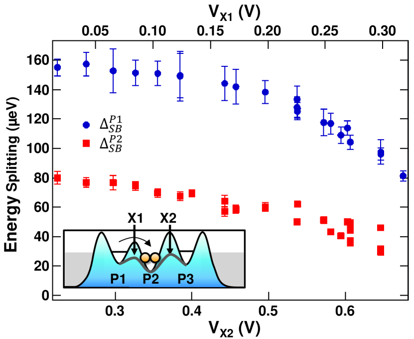
We now use this technique to measure how changes in confining potential affect of dots and . We sweep the bias voltages on gates and at a constant ratio, as indicated by the bottom and top axes of Fig. 3, to deform the confinement potentials while maintaining interdot tunnel couplings amenable to SCC. We observe that the energy splittings for each dot decrease with bias voltage by a factor of 2, with maximum values of eV for and eV for . We can rule out a continuous variation of the gate-dot lever arm as the source of this effect (see Supplemental Section I) and conclude that the underlying energy splitting is changing.
Identifying the physics responsible for this variation is challenging but important to improve device performance. The relatively smooth, correlated change in over a wide range of biases suggests that valley splitting alone is not responsible: shifting wave functions would sample disorder at the interface of a SiGe alloy in a more random fashion Abadillo-Uriel et al. (2018); Zhang et al. (2013). Also unlikely is an arrangement of steps that would cause valley splittings to change with bias on distinct dots at nearly the same rateFriesen et al. (2007). Vertical electric fields easily tune valley splitting in MOS Si quantum dots Yang et al. (2013); Gamble et al. (2016), but the effect is much weaker in Si/SiGe, especially when controlled by neighboring barrier gates. We therefore posit that in this case, the most likely cause of the change in with bias is a modification of the two-electron orbital confinement energy, i.e., the wave functions become more elliptical with forward bias on the barrier gates Melnikov and Leburton (2006); Hanson et al. (2007). We note that valley-orbit hybridization is also possible and could be the cause of an apparent saturation in at tighter confinements Friesen and Coppersmith (2010). Even though we believe that this device is limited by orbital splittings, we expect valley splittings to be similar in magnitudeNeyens et al. (2018). The delicate interplay between these two degrees of freedom necessitates an measurement technique as described here.
In summary, we have described an excited-state spectroscopy method for measuring the two-electron ground-to-excited state energy separation of quantum dots. The measured energy splitting is directly relevant to state preparation and measurement of singlet/triplet based qubits. This technique, which is only suitable in systems where charge measurements are possible within spin , is applied to quantum dots tuned for spin-to-charge conversion. In showing the tunability of with confinement gate bias, we demonstrate the utility of this technique in optimizing device performance. This measurement technique should be useful to all quantum dot architectures that require robust spin-blockade.
The authors gratefully acknowledge T. Ladd, M. Gyure, M. Reed, A. Pan, D. Kim for helpful discussions.
References
- Ladd and Carroll (2018) Thaddeus D. Ladd and Malcolm S. Carroll, “Silicon qubits,” in Encyclopedia of Modern Optics (Second Edition), edited by Bob D. Guenther and Duncan G. Steel (Elsevier, Oxford, 2018) second edition ed., pp. 467 – 477.
- Muhonen et al. (2014) Juha T. Muhonen, Juan P. Dehollain, Arne Laucht, Fay E. Hudson, Rachpon Kalra, Takeharu Sekiguchi, Kohei M. Itoh, David N. Jamieson, Jeffrey C. McCallum, Andrew S. Dzurak, and Andrea Morello, “Storing quantum information for 30 seconds in a nanoelectronic device,” Nature Nanotechnology 9, 986 (2014).
- Eng et al. (2015) Kevin Eng, Thaddeus D. Ladd, Aaron Smith, Matthew G. Borselli, Andrey A. Kiselev, Bryan H. Fong, Kevin S. Holabird, Thomas M. Hazard, Biqin Huang, Peter W. Deelman, Ivan Milosavljevic, Adele E. Schmitz, Richard S. Ross, Mark F. Gyure, and Andrew T. Hunter, “Isotopically enhanced triple-quantum-dot qubit,” Science Advances 1 (2015), 10.1126/sciadv.1500214.
- Yoneda et al. (2018) Jun Yoneda, Kenta Takeda, Tomohiro Otsuka, Takashi Nakajima, Matthieu R. Delbecq, Giles Allison, Takumu Honda, Tetsuo Kodera, Shunri Oda, Yusuke Hoshi, Noritaka Usami, Kohei M. Itoh, and Seigo Tarucha, “A quantum-dot spin qubit with coherence limited by charge noise and fidelity higher than 99.9%,” Nature Nanotechnology 13, 102–106 (2018).
- Reed et al. (2016) M. D. Reed, B. M. Maune, R. W. Andrews, M. G. Borselli, K. Eng, M. P. Jura, A. A. Kiselev, T. D. Ladd, S. T. Merkel, I. Milosavljevic, E. J. Pritchett, M. T. Rakher, R. S. Ross, A. E. Schmitz, A. Smith, J. A. Wright, M. F. Gyure, and A. T. Hunter, “Reduced sensitivity to charge noise in semiconductor spin qubits via symmetric operation,” Phys. Rev. Lett. 116, 110402 (2016).
- Martins et al. (2016) Frederico Martins, Filip K. Malinowski, Peter D. Nissen, Edwin Barnes, Saeed Fallahi, Geoffrey C. Gardner, Michael J. Manfra, Charles M. Marcus, and Ferdinand Kuemmeth, “Noise suppression using symmetric exchange gates in spin qubits,” Phys. Rev. Lett. 116, 116801 (2016).
- Veldhorst et al. (2014) M. Veldhorst, J. C. C. Hwang, C. H. Yang, A. W. Leenstra, B. de Ronde, J. P. Dehollain, J. T. Muhonen, F. E. Hudson, K. M. Itoh, A. Morello, and A. S. Dzurak, “An addressable quantum dot qubit with fault-tolerant control-fidelity,” Nature Nanotechnology 9, 981 EP – (2014).
- Muhonen et al. (2015) J T Muhonen, A Laucht, S Simmons, J P Dehollain, R Kalra, F E Hudson, S Freer, K M Itoh, D N Jamieson, J C McCallum, A S Dzurak, and A Morello, “Quantifying the quantum gate fidelity of single-atom spin qubits in silicon by randomized benchmarking,” Journal of Physics: Condensed Matter 27, 154205 (2015).
- Fogarty et al. (2017) M. A. Fogarty, K. W. Chan, B. Hensen, W. Huang, T. Tanttu, C. H. Yang, A. Laucht, M. Veldhorst, F. E. Hudson, K. M. Itoh, D. Culcer, A. Morello, and A. S. Dzurak, “Integrated silicon qubit platform with single-spin addressability, exchange control and robust single-shot singlet-triplet readout,” arXiv:1708.03445 (2017).
- Kawakami et al. (2016) Erika Kawakami, Thibaut Jullien, Pasquale Scarlino, Daniel R. Ward, Donald E. Savage, Max G. Lagally, Viatcheslav V. Dobrovitski, Mark Friesen, Susan N. Coppersmith, Mark A. Eriksson, and Lieven M. K. Vandersypen, “Gate fidelity and coherence of an electron spin in an si/sige quantum dot with micromagnet,” Proceedings of the National Academy of Sciences 113, 11738–11743 (2016), http://www.pnas.org/content/113/42/11738.full.pdf .
- Zajac et al. (2017) D. M. Zajac, A. J. Sigillito, M. Russ, F. Borjans, J. M. Taylor, G. Burkard, and J. R. Petta, “Resonantly driven cnot gate for electron spins,” Science (2017), 10.1126/science.aao5965.
- Yang et al. (2018) C. H. Yang, K. W. Chan, R. Harper, W. Huang, T. Evans, J. C. C. Hwang, B. Hensen, A. Laucht, T. Tanttu, F. E. Hudson, S. T. Flammia, K. M. Itoh, A. Morello, S. D. Bartlett, and A. S. Dzurak, “Silicon qubit fidelities approaching stochastic noise limits via pulse optimisation,” arXiv:1807.09500 (2018).
- Huang et al. (2018) W. Huang, C. H. Yang, K. W. Chan, T. Tanttu, B. Hensen, R. C. C. Leon, M. A. Fogarty, J. C. C. Hwang, F. E. Hudson, K. M. Itoh, A. Morello, A. Laucht, and A. S. Dzurak, “Fidelity benchmarks for two-qubit gates in silicon,” (2018), arXiv:1805.05027 .
- Veldhorst et al. (2015) M. Veldhorst, C. H. Yang, J. C. C. Hwang, W. Huang, J. P. Dehollain, J. T. Muhonen, S. Simmons, A. Laucht, F. E. Hudson, K. M. Itoh, A. Morello, and A. S. Dzurak, “A two-qubit logic gate in silicon,” Nature 526, 410 (2015).
- Watson et al. (2018) T. F. Watson, S. G. J. Philips, E. Kawakami, D. R. Ward, P. Scarlino, M. Veldhorst, D. E. Savage, M. G. Lagally, Mark Friesen, S. N. Coppersmith, M. A. Eriksson, and L. M. K. Vandersypen, “A programmable two-qubit quantum processor in silicon,” Nature 555, 633 (2018).
- Hanson et al. (2007) R. Hanson, L. P. Kouwenhoven, J. R. Petta, S. Tarucha, and L. M. K. Vandersypen, “Spins in few-electron quantum dots,” Rev. Mod. Phys. 79, 1217–1265 (2007).
- Gamble et al. (2016) John King Gamble, Patrick Harvey-Collard, N. Tobias Jacobson, Andrew D. Baczewski, Erik Nielsen, Leon Maurer, Inès Montaño, Martin Rudolph, M. S. Carroll, C. H. Yang, A. Rossi, A. S. Dzurak, and Richard P. Muller, “Valley splitting of single-electron si mos quantum dots,” Applied Physics Letters 109, 253101 (2016), https://doi.org/10.1063/1.4972514 .
- Boykin et al. (2004) Timothy B. Boykin, Gerhard Klimeck, M. A. Eriksson, Mark Friesen, S. N. Coppersmith, Paul von Allmen, Fabiano Oyafuso, and Seungwon Lee, “Valley splitting in strained silicon quantum wells,” Applied Physics Letters 84, 115–117 (2004), https://doi.org/10.1063/1.1637718 .
- Melnikov and Leburton (2006) Dmitriy V. Melnikov and Jean-Pierre Leburton, “Dimensionality effects in the two-electron system in circular and elliptic quantum dots,” Phys. Rev. B 73, 085320 (2006).
- Sasaki et al. (2009) Kohei Sasaki, Ryuichi Masutomi, Kiyohiko Toyama, Kentarou Sawano, Yasuhiro Shiraki, and Tohru Okamoto, “Well-width dependence of valley splitting in si/sige quantum wells,” Applied Physics Letters 95, 222109 (2009), https://doi.org/10.1063/1.3270539 .
- Zhang et al. (2013) Lijun Zhang, Jun-Wei Luo, Andre Saraiva, Belita Koiller, and Alex Zunger, “Genetic design of enhanced valley splitting towards a spin qubit in silicon,” Nature Communications 4, 2396 (2013), article.
- Neyens et al. (2018) Samuel F. Neyens, Ryan H. Foote, Brandur Thorgrimsson, T. J. Knapp, Thomas McJunkin, L. M. K. Vandersypen, Payam Amin, Nicole K. Thomas, James S. Clarke, D. E. Savage, M. G. Lagally, Mark Friesen, S. N. Coppersmith, and M. A. Eriksson, “The critical role of substrate disorder in valley splitting in si quantum wells,” Applied Physics Letters 112, 243107 (2018), https://doi.org/10.1063/1.5033447 .
- van der Wiel et al. (2002) W. G. van der Wiel, S. De Franceschi, J. M. Elzerman, T. Fujisawa, S. Tarucha, and L. P. Kouwenhoven, “Electron transport through double quantum dots,” Rev. Mod. Phys. 75, 1–22 (2002).
- Mi et al. (2017) X. Mi, Csaba G. Péterfalvi, Guido Burkard, and J. R. Petta, “High-resolution valley spectroscopy of si quantum dots,” Phys. Rev. Lett. 119, 176803 (2017).
- Schoenfield et al. (2017) Joshua S. Schoenfield, Blake M. Freeman, and HongWen Jiang, “Coherent manipulation of valley states at multiple charge configurations of a silicon quantum dot device,” Nature Communications 8, 64 (2017).
- Lim et al. (2011) W H Lim, C H Yang, F A Zwanenburg, and A S Dzurak, “Spin filling of valley–orbit states in a silicon quantum dot,” Nanotechnology 22, 335704 (2011).
- Borselli et al. (2011) M. G. Borselli, K. Eng, E. T. Croke, B. M. Maune, B. Huang, R. S. Ross, A. A. Kiselev, P. W. Deelman, I. Alvarado-Rodriguez, A. E. Schmitz, M. Sokolich, K. S. Holabird, T. M. Hazard, M. F. Gyure, and A. T. Hunter, “Pauli spin blockade in undoped si/sige two-electron double quantum dots,” Applied Physics Letters 99, 063109 (2011), https://doi.org/10.1063/1.3623479 .
- Friesen and Coppersmith (2010) Mark Friesen and S. N. Coppersmith, “Theory of valley-orbit coupling in a si/sige quantum dot,” Phys. Rev. B 81, 115324 (2010).
- Shi et al. (2011) Zhan Shi, C. B. Simmons, J. R. Prance, John King Gamble, Mark Friesen, D. E. Savage, M. G. Lagally, S. N. Coppersmith, and M. A. Eriksson, “Tunable singlet-triplet splitting in a few-electron si/sige quantum dot,” Applied Physics Letters 99, 233108 (2011), https://doi.org/10.1063/1.3666232 .
- Yang et al. (2013) C. H. Yang, A. Rossi, R. Ruskov, N. S. Lai, F. A. Mohiyaddin, S. Lee, C. Tahan, G. Klimeck, A. Morello, and A. S. Dzurak, “Spin-valley lifetimes in a silicon quantum dot with tunable valley splitting,” Nature Communications 4, 2069 EP – (2013), article.
- Lai et al. (2011) N. S. Lai, W. H. Lim, C. H. Yang, F. A. Zwanenburg, W. A. Coish, F. Qassemi, A. Morello, and A. S. Dzurak, “Pauli spin blockade in a highly tunable silicon double quantum dot,” Scientific Reports 1, 110 (2011), article.
- Borselli et al. (2015) M. G. Borselli, K. Eng, R. S. Ross, T. M. Hazard, K. S. Holabird, B. Huang, A. A. Kiselev, P. W. Deelman, L. D. Warren, I. Milosavljevic, A. E. Schmitz, M. Sokolich, M. F. Gyure, and A. T. Hunter, “Undoped accumulation-mode si/sige quantum dots,” Nanotechnology 26, 375202 (2015).
- Zajac et al. (2015) D. M. Zajac, T. M. Hazard, X. Mi, K. Wang, and J. R. Petta, “A reconfigurable gate architecture for si/sige quantum dots,” Applied Physics Letters 106, 223507 (2015), https://doi.org/10.1063/1.4922249 .
- Ward et al. (2016) Daniel R. Ward, Dohun Kim, Donald E. Savage, Max G. Lagally, Ryan H. Foote, Mark Friesen, Susan N. Coppersmith, and Mark A. Eriksson, “State-conditional coherent charge qubit oscillations in a si/sige quadruple quantum dot,” Npj Quantum Information 2, 16032 (2016), article.
- Studenikin et al. (2018) S. A. Studenikin, L. Gaudreau, K. Kataoka, D. G. Austing, and A. S. Sachrajda, “Enhancement-mode two-channel triple quantum dot from an undoped si/si0.8ge0.2 quantum well hetero-structure,” Applied Physics Letters 112, 233101 (2018), https://doi.org/10.1063/1.5023596 .
- Zajac et al. (2016) D. M. Zajac, T. M. Hazard, X. Mi, E. Nielsen, and J. R. Petta, “Scalable gate architecture for a one-dimensional array of semiconductor spin qubits,” Phys. Rev. Applied 6, 054013 (2016).
- Deelman et al. (2016) Peter W. Deelman, Lisa F. Edge, and Clayton A. Jackson, “Metamorphic materials for quantum computing,” MRS Bulletin 41, 224–230 (2016).
- Kane (1998) B. E. Kane, “A silicon-based nuclear spin quantum computer,” Nature 393, 133 (1998), article.
- DiCarlo et al. (2004) L. DiCarlo, H. J. Lynch, A. C. Johnson, L. I. Childress, K. Crockett, C. M. Marcus, M. P. Hanson, and A. C. Gossard, “Differential charge sensing and charge delocalization in a tunable double quantum dot,” Phys. Rev. Lett. 92, 226801 (2004).
- Vink et al. (2007) I. T. Vink, T. Nooitgedagt, R. N. Schouten, L. M. K. Vandersypen, and W. Wegscheider, “Cryogenic amplifier for fast real-time detection of single-electron tunneling,” Applied Physics Letters 91, 123512 (2007).
- Abadillo-Uriel et al. (2018) J. C. Abadillo-Uriel, B. Thorgrimsson, D. Kim, L. W. Smith, C. B. Simmons, D.R. Ward, R.H. Foote, J. Corrigan, D. E. Savage, M. G. Lagally, M. J. Calderón, S. N. Coppersmith, M. A. Eriksson, and M. Friesen, “Signatures of atomic-scale structure in the energy dispersion and coherence of a si quantum-dot qubit,” (2018), arXiv:1805.10398 .
- Friesen et al. (2007) Mark Friesen, Sucismita Chutia, Charles Tahan, and S. N. Coppersmith, “Valley splitting theory of quantum wells,” Phys. Rev. B 75, 115318 (2007).