Ultrafast Bessel beams; advanced tools for laser materials processing
Abstract
Ultrafast Bessel beams demonstrate a significant capacity of structuring transparent materials with high degree of accuracy and exceptional aspect ratio. The ability to localize energy on the nanometer scale (bypassing the 100 nm milestone) makes them ideal tools for advanced laser nanoscale processing on surfaces and in the bulk. This allows to generate and combine micron and nano-sized features into hybrid structures that show novel functionalities. Their high aspect ratio and the accurate location can equally drive an efficient material modification and processing strategy on large dimensions. We review here the main concepts of generating and using Bessel non-diffractive beams and their remarkable features, discuss general characteristics of their interaction with matter in ablation and material modification regimes, and advocate their use for obtaining hybrid micro and nanoscale structures in two and three dimensions performing complex functions. High throughput applications are indicated. The example list ranges from surface nanostructuring and laser cutting to ultrafast laser welding and the fabrication of three dimensional photonic systems embedded in the volume.
I Introduction
Nowadays micro/nano- technologies are critically dependent on the development of precise and controllable processing tools able to structure materials with utmost precision and reduced collateral damage. Ultrashort laser processing has thus developed into a performant technology able to take up this challenge, with intrinsic processing capabilities well into the nanoscale Mis06 ; Sug14 ; Sug17 ; MM07 , approaching and even surpassing the 100 nm scale Jog04 . This relies on unmatched abilities to process materials using nonlinear excitation and limited thermal diffusion, generating high-end applications where energy localization in space and time by ultrashort pulses is critical. To optimize structuring in terms of yield, quality, and scale, new concepts of smart laser material processing have emerged, based on the spatio-temporal design of irradiation according to the material response Stoi03 ; Stoi10 ; Bau07 ; Lu13 . An advanced processing strategy requires in-depth understanding of the irradiation and material transformation process, with the ability to synergetically correlate irradiation and material reaction to energy load. The geometry is equally important to increase processing efficiency and precision, and automated procedures of pulse spatial tailoring emerged and developed Mau09 ; Has09 ; Boo11 ; Has14 ; Zh16a , taking advantage of the geometry of interaction. These involve either shaping geometrically the interaction region in relevant forms, corrected aberration-free beam delivery, parallel processing procedures on user-designed patterns, or three dimensional patterning of transverse intensity profiles along the propagation axis Mau09 ; Has14 ; Zh16a ; Cour04 ; San05 ; Wil98 ; Mau08 . Coupled spatio-spectral and spatio-temporal approaches have permitted to downsize and sculpt the focal region for the highest accuracy He10 ; Squ10 ; Boo18 . These take benefit of the large spectral content inherent to a short pulse by spatially and temporally locking the frequencies only at the interaction site. Polarization features can be designed spatially and temporally Has13 ; Brix01 . All together, by engineering in space, time, and vectorial domains, Stoi10 ; Has14 ; Amo17 ; Pad04 , light confinement can harness key features of interaction with matter and build-up unique material transformation paths with highest precision. This is key in designing materials and functions, upscaling approaches for accurate and flexible processing.
Within these developments, recently a new class of ultrafast laser beams emerged for materials processing applications in ultrafast modes Sch10 ; BD10 , with potential in attaining processing accuracy beyond diffraction limit, well into the nanoscale domain. These relies on non-diffractive concepts; particularly the Bessel-Gauss beams McL54 ; Dur87 ; Wig91 , where the interaction section can be multidimensionally designed using non-diffractive propagation. The potential of these Bessel-Gauss beams (hereafter called Bessel beams for simplicity) is fully exploitable in transparent materials, with an energy gap superior to the photon energy. Here dielectrics represent a considerable field of action in view of their technological importance in optics, telecom, micro-electronics, or precision mechanics. Application concepts have swiftly emerged in laser structuring, dicing, drilling, in the development of embedded optical elements Juod01 ; Juod13 ; Sug17b ; Lu15 ; Mey17 ; Ahn18 ; Yan17 ; Mit15 ; Zam09 ; Wa16 ; Dud17 in optical materials, or in the precise interaction with biological tissues Dho07 .
We will review here some of the recent results of ultrafast zero-order Bessel beam applications in material processing, particularly for transparent materials. The benefits of these elongated beams that exceed the Gaussian Rayleigh range by several orders of magnitude for laser micro and nano-processing will be outlined. We will briefly discuss generation concepts, major physical aspects of laser-material interaction in non-diffractive modes and the way to control energy deposition. We indicate several promising applications fields in deep drilling, dielectric cleaving and cutting, materials welding, and the generation of hybrid micro and nanoscale features for embedded photonic devices BD10 ; BS14 ; Rapp17 ; Zh18 ; Zh16 ; Zh18b ; Mar17 with applications in spectroscopy and sensing.
II Bessel beam interaction with matter
II.1 Bessel beam generation
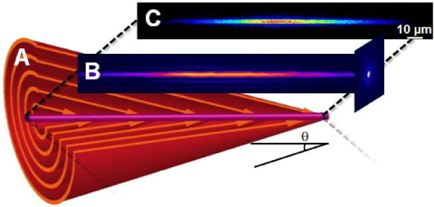
Several methods for generating non-diffractive Bessel beams (for an extended review see DA12 and the references therein) rely on conical intersection of wavefronts generated by either a conical phase (axicon, spatial light modulator) and subsequent refraction or diffraction, or by the convergence of annular beams with non-varying polarization. The first approach is among the most utilised as it harnesses most of the input energy of the incident Gauss pulse on the transformation optical element. The phase synchronization and interference of the incoming wavefronts after conical refraction generates an elongated central core of light on distances well beyond of what can be achieved normally by focusing Gauss pulses (i.e. confocal distance), creating the so-called non-diffractive appearance. The core is surrounded by a series of rings given by the higher orders of interference of the conically converging wavefronts. Due to the conical geometry the circular lobes serve as a continuous energy reservoir for the core, feeding its development and favoring a remarkable stability. Depending on the convergence angle and the lateral size of the input beam, the core can develop on significant distances. This axial elongation can be simply seen as a shadow projected on the axis of the initial Gauss transverse dimension (waist) after the conical refraction, or more precisely as the geometrical places where the spatially-limited sweeping front crosses the propagation axis. For practical applications, extremely high aspect ratios can be obtained (), where both the elongation () and the diameter () of the core are defined by the conical angle (, , with being the wave-vector). The axial distribution can be further modulated using apodizing techniques Ciz09 . The created beam can be re-imaged, demagnified and steered to the workpiece by relay optics Bh17b , with micron-sized cores and aspect ratios exceeds easily a factor 100 in processing conditions. Uniform distributions can be achieved by spectral filtering the leakage from non-ideal axicon tips Bh17b . These non-diffractive beams are nonlinearly stable Gad01 ; FT12 , robust, as the core is continuously supplied with photons, and less affected by spherical aberrations. This is an essential difference between Gaussian and Bessel illumination that lies in the nonlinear propagation regime. While at ablation-level intensities, Gaussian beams undergo strong Kerr self-focusing and plasma defocusing, resulting in the complex spatio-temporal reshaping, Bessel beams can sustain a more stable propagation-invariant regime Pol08 . The latter is possible for sufficiently high conical angles, and has also been extended to Bessel vortices Xie15 .
Examples of Bessel beam generation are represented in Figure 1, with a conceptual scheme of conical intersection given in Figure 1A, an optically reconstructed beam via sectional transverse imaging (Figure 1B) and a plasma trace in air generated by a corresponding Bessel beam (Figure 1C), witness of the strong ionization capability of these beams. Most of the discussions below pertain to the wavelength of 800 nm (Ti:Sapphire laser technology), with few examples at other wavelengths, specified in the text.
The relevant structuring features are related to the dimensional characteristics of the Bessel beams; the high aspect ratio of the intensity distribution with narrow transverse distributions, as well as to its symmetry. Deep and large area structuring can be foreseen. These light longitudinal patterns are versatile enough to allow a distribution of field intensity with a symmetry easily controllable by simple optical transformations Dud18 . Techniques of programmable amplitude and phase manipulation can exercise further control on the Bessel beams in terms of contrast and uniformity Ciz09 . The energy ratio between the core and the lobes can equally be engineered (for example by coherently superposing two Bessel distribution via an annular binary aperture), allowing to concentrate more energy on the core, while still retaining a range of non-diffractive elongation Mo15 . A core-lobe contrast reduction from 16% to 4% was demonstrated, trading off the aspect ratio. Recently, concepts of multiplexing Bessel beams have been developed to enhance the structuring throughput Yu16 with parallel approaches. Some of these shaping possibilities will be indicated below with respect to the relevant application.
II.2 Interaction of ultrafast Bessel beams with transparent materials
Due to its interferential nature, the Bessel beam represents a quasi-stationary axial light distribution, where an apparent superluminal front evolution (in case of an axicon) is given by the axial projection of the incoming wavefronts. The ultrashort time envelope and the resulting intensity ensure in a dielectric material carrier excitation via multiphoton processes and collisional multiplication It06 . The order of the nonlinear absorption is simply defined by the number of photons required to bridge the material forbidden band energy gap. The laser energy is deposited in a free carrier plasma and then relaxes to the host material matrix. Depending on the degree of excitation, the energy can be transferred to the matrix by electronically-induced structural effects intermediated by bond breaking at sub-critical plasma densities, or, if a threshold in the plasma density is achieved, via collisional vibrational activation (electron-phonon coupling), heating, and evolution towards the liquid and the gas phase. Characteristic to the Bessel distribution, the high pressure high temperature state achieved in the material exposed volume relaxes perpendicular to the beam axis. If the internal pressure exceeds the mechanical resistance of the material, shock and rarefaction occurs ST06 , compressing the material to the sides and opening axially a low density phase on the trace of the Bessel core. This is a main difference with respect to Gauss beams which on surfaces evacuate the ablated material and in the bulk preserve the symmetry of the energy deposition geometry. Depending on the pressure level, the opening may occur in the solid or in the liquid phase. As the size of the modification is defined then by cavitation and material rupture due to stress gradients, the size can be considerably smaller than the beam waist, enabling structuring below diffraction limit and making accessible the nanoscale. Similar sizes will occur also in the event of gas-phase nucleation, provided that the thermodynamic conditions are favorable. These aspects were recently addressed in Refs. VS16 ; RC16 ; Bh17 for Bessel geometries.
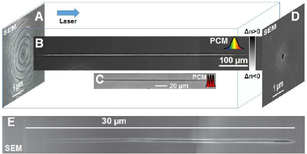
It is first of interest to discuss the Bessel irradiation case of a model glass material such as fused silica (a-SiO2). The types of laser-induced modification range from positive index changes to one-dimensional void generation. Examples VS16 ; Bh17 are given in Figure 2. The material morphology and the geometry of the modification are controllable via the pulse duration and via the Bessel cone angle (subject to refraction in the bulk). Short pulse durations in the bulk and at low and moderate focusing conditions favor via self-limiting effects soft positive index modification (in the – range) MS13 with interest in developing large core waveguiding elements DH96 . This is mainly the consequence of a more compact structural rearrangement of matter following bond-breaking Krol03 . Multiple pulses can determine the spontaneous onset of regular nanostructures Kaz08 ; Rud17 . Of interest for material structuring from this work’s perspective is a different regime. Stretched laser pulses or tight focusing geometries can overcome diffraction and defocusing and determine strong heating and hydrodynamic movement of the material, opening thus a void. Volume void generation is usually assimilated to micro-explosions GM97 . Depending on the position of the Bessel beam, structures can be generated on the input surface, in the bulk, or at the exit surface. These cases are presented in Figure 2A–E, with examples on single laser shot effects on silica surfaces given in Figure 2A, volume structures in silica shown in Figure 2B,C, and exit surface patterns depicted in Figure 2D. Scanning electron and phase contrast microscopy techniques were used to visualize the structuring results. A further example of bulk void modification in sapphire is given in Figure 2E.
Processing the input surface (Figure 2A) has the drawback of imprinting the side annular structures, even in the presence of a nonlinear excitation of a higher order. This limits the applicability to energies not significantly exceeding the damage threshold at the core location. Efforts are being made to reduce their impact by further engineering the phase of the Bessel beam Sug17b . Equally, multistep irradiation and etching techniques can be applied Wang18 below the irradiation threshold to enable efficient structuring, where pulse temporal engineering can play a role.
This artefact goes away when considering bulk interactions. The generation of a transient carrier population creates presumably phase instabilities that leads to a dynamic delocalization of the rings, where the optical path difference changes from the condition , with . In a general way this suggest indirectly potential beam reshaping due to nonlinearities, cleaning the laser pulse. This fact can increase the processing window where structures can be made before the lobes can be problematic. Figure 2B,C shows bulk interactions for generating voids, respectively refractive index changes in bulk fused silica. The back (exit) surface processing (Figure 2D) preserves this self-cleaning of the pulse, exhibiting structures with cross-sections below the micron level without visible side effects. Note that a similar energy was used in Figure 2A and Figure 2D, many times above the surface threshold, albeit the different pulse duration and focusing conditions (=0.5 J for tightly focused 60 fs pulses and =2.5 J for moderately focused 2 ps pulses). Sizes even below 100 nm can be currently achieved VS16 . This shows a strong potential for processing that will be outlined below. This response is not limited to glass but pertains equally for hard crystalline materials, with an example of a nanovoid in sapphire being shown in Figure 2E RC16 . The technique can be applied to generate through holes in a single shot event, with high reliability and efficiency.
III Bessel beam material structuring
III.1 Deep surface interaction
The above considerations lay down a concept of deep processing of transparent materials where the depth of structuring is precisely defined by the position of the Bessel beam and the processing size represents a record in terms of resolution and aspect ratio BD10 . Surface and bulk interaction processes can be precisely defined, with surface interactions defining a processing window for deep, high aspect ratio drilling as required by specific applications. Micron-sized and sub-micron-sized structures can be patterned, with the depth adjustable by the beam localization with respect to the surface. If input surface interactions present limitations in terms of usable energy range without extended collateral damage, the back surface processing represents a viable strategy for morphing surfaces in depth, minimizing the lobe influence on the damage aspect.
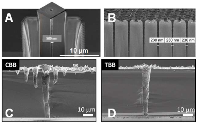
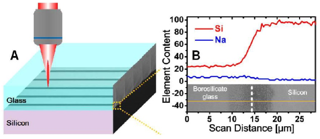
Figure 3A,B represents an example where two types of glasses are deep-processed on the back surface; Corning 7980-5F fused silica and Corning 0211 borosilicate glass. The result points out the extraordinary precision and aspect ratio achievable with ultrashort and short Bessel beams; a robust pathway to nanostructuring with potential applications. Liquid immersion can be used to remove debris. The scales attainable with this technology are potentially interesting to generate efficient surface functions and optical response in the near and mid-infrared spectral regions. For surface interaction the lobe contrast may pose limitations to the spatial confinement of the damage at high processing fluences due to a first lobe contrast of almost 16 %. A method of lobe contrast engineering and Bessel tailoring based on a binary phase was proposed in Sug17b , conceptually similar to the Bessel superposition method from Mo15 , but, due to the phase modulation approach, more energy efficient. An achieved contrast of 0.6% was reported while keeping the elongation at sufficient values to outpace Gaussian performance. Thus high quality through vias of several tens of microns diameter were demonstrated in silicon layers for three-dimensional integrated circuits using a 1.5 m ultrashort tailored Bessel beam, with photon energies below the gap. The result is illustrated in Figure 3C,D. Recently, ultrafast Bessel beams were applied to achieve through-structuring in diamond based on a laser-induced graphitization process all along the irradiation path Trap17 .
III.2 Laser cleaving and cutting
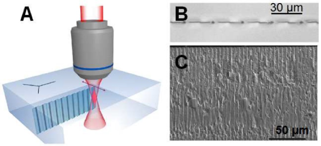
The irradiation concept outlined above can be extended to a different application that has a significant technological potential; laser cleaving and cutting of glasses and crystals, where particular care is needed in view of their brittleness. It is to be noted that glass structuring Itoh14 (and more generally structuring of inorganic transparent materials) represents an important market for displays in consumer electronics or for medical devices as glass shows optical, mechanical and chemical properties of interest. The non-diffractive class of beam is particularly interesting as it can induce large aspect ratio in-volume (ablation-free) modifications of transparent materials for what is called stealth machining Kuma07 and it can define a promising pathway to glass separation technologies. Figure 4 gives several examples of laser cleaving of dielectric materials Mey17 ; Rapp17 using Bessel beams, with an experimental scheme depicted in Figure 4A. The idea behind is to generate a separation path by weakening directionally the bonding strength in the material with the help of an elongated beam. In sapphire (Figure 4B), a material of technological importance in displays, high-speed cleaving can be obtained with successive micron spaced Bessel pulses. Ultrashort pulses with controllable polarization direction can induce directional cracks that propagate between impact points, initiating the cleaving process Rapp17 . The relative orientation to the crystallographic axis and the scan directions are control knobs for the development of the cracks as they define stress fields. Bessel beams allow for creating homogeneous damages all along the depth of the material, where the control on the crack formation enables the processing of a continuous fracture plane, used for the sapphire separation. This opens the route for high speed processing and separation of crystalline substrates. This method, applicable to brittle materials, can combine non-diffractive spatial techniques with temporally-controlled pulse sequences (bursts, tunable envelopes, tunable repetition rates) for a substantial process control Mish17 ; Mish16 . This involves tuning the energy deposition for initiating the process while avoiding catastrophic uncontrollable damage or excess heat loading. Recent reports integrated Bessel beam irradiation with additional engineering features (e.g. tilted fronts) to respond to process requirements, for example defining inner contours Nolte17 . Tilting the axicon can be equally a source of controlling stability and ellipticity, providing an additional element of control Dud18 in dicing techniques. All these methods can be applied successfully to a large range of crystalline and glassy material by creating directional separation planes.
In isotropic materials, an anisotropy, advantageous for cutting, can be induced by a geometrical transverse deformation of the beam Mey17 ; Dud16 affecting the transverse symmetry of the beam along a preferential axis. The associated asymmetric distribution of mechanical constraints will define a plane of separation. An example of a borosilicate glass sample cleaved by elliptical beams Mey17 is given in Figure 4C. The asymmetric beam can successfully perform the cleaving operation based on channel drilling, favoring a preferential axis, without relating to sub-ablation directional stress planes Mey17 . This represents a novel transverse beam shaping method of non-diffracting beams that can yield a propagation invariant regime at ablation-level intensities. The approach generates elliptical nanochannels in glass after single-shot illumination and the property can be used to guide material cleaving with sub-micron precision.
It is worth noting that the techniques started to acquire a visible industrial dimension, in particular for dicing, cutting, and separation of glassy and crystalline substrates. Patented and patent-pending applications developed at major laser and equipment providers access now a market in full development.
III.3 Welding with ultrafast laser Bessel beams
A straightforward advantage of non-diffractive beams and their longitudinally elongated core on tens and hundreds of microns is the relaxation of the positioning conditions in processing regimes. The energy can be brought to the impact point without precise focusing and positioning Zh18 approaches. This can be of significant advantage in processing applications, particularly when non-planar surfaces are required or small features (surface nanoprocessing Cou09 ; Sah14 ), but equally in a different application related to material joining and welding on microscales, where energy has to be precisely transported at the interface Miy07 . Microwelding occurs point by point or line by line by scanning the laser spot along the contact interface, where nonlinear absorption occurs to heat and change locally the materials. This requires specifically an accurate laser beam focusing and positioning onto the samples contact interface, a challenge for Gauss beams with micron-sized Rayleigh range. Therefore benefits are expectable for ultrafast Bessel material welding including of dissimilar materials. Figure 5A,B shows an example of ultrafast Bessel beam welding of silicon and borosilicate glass (Schott D 263) in optical contact, where the energy is transported across the glass layer to the interface between the materials, with a schematics of the approach shown in Figure 5A. The image (SEM) of the affected zone is given in Figure 5B together with elemental analysis across the interface in the impact region. Elemental mixing occurs thorough the interface driven by thermal and material flow. The focal-position tolerant zone for efficient welding was reported to increase 5.5-fold by using zero-order Bessel beam processes as compared to Gaussian beam welding Zh18 . Shear joining strengths as high as 16.5 MPa were obtained, superior to the Gauss case for similar sizes of processed domains.
We indicate that welding techniques for transparent or dissimilar material are now developed in industrial application by major laser and equipment developers.
III.4 Hybrid structures for 3D photonics
The discussion above has outlined the irradiation conditions for obtaining stable uniform one-dimensional nanovoids or domains of positive index change. These are equivalent to objects of low or high dielectric constant that can be positioned in space. Thus a potential field of interest is related to a high-end application related to 3D photoinscription and development of photonic components using ultrafast lasers, based on concepts of refractive index engineering. The potential for optical functions has been early recognized and optical elements were already tested for fabrication. Putting forward the achievable symmetry, waveguides were photoinscribed using ultrashort Bessel beams Zam09 . A natural extension of Bessel beam irradiation with respect to the geometrical characteristics, notably the longitudinal elongation, is the fabrication of volume gratings Juod13 in transparent materials that show high diffraction efficiency. A recent technique that combines Bessel irradiation with thermal treatment was recently reported for high efficacy volume gratings in photo-thermo-refractive glass Zh16 , where the index changes is delivered via a local crystallization of the glass structure. An example of as-fabricated volume gratings is given in Figure 6A, showing diffraction efficiency exceeding 90 Zh16 .
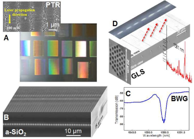
Furthermore, a potentially interesting feature of Bessel beam structures comes from their transverse size that can go on the 100 nm scale VS16 . Combined with the one dimensional aspect, this feature can be used to sample electrical fields in optical systems, for example in embedded waveguides (e.g. nano-scatterers or nano-diffractors) and create efficient optical functions combining hybrid micro and nanoscale structures. Figure 6B,C depicts an example of waveguide Bragg gratings fabricated point by point Marsh06 by short Bessel pulses in an ultrafast laser photoinscribed waveguide in bulk fused silica Zh18b , with its spectral response. A beam at 1030 nm central wavelength was used to create single pulse sequential nanovoids crossing the section of the guide. The structured waveguide exhibits a highly efficient optical resonance in transmission, of 40 dB/cm at 1550 nm in the third order. Ps microjoule laser pulses at 1030 nm incident wavelength were used to generate uniform nanoscale voids positioned with sub-micron accuracy, enabling also the fabrication of first order gratings and tunable coupling. Bragg resonances in embedded optical waveguides are essential elements for developing mechanically stable optical networks, lasers, and sensing systems for pressure and temperature.
Nanoscale sampling equally allows for the optical reconstruction of light fields with high fidelity by locally scattering field components. The scattering cross-section can be defined by the geometrical section of the Bessel-induced objects and the associated index step. Bessel nanovoids arrays with geometrical sections in the 100 nm range form thus highly efficient scatterers. Optical field reconstruction is thus of interest and recent applications in astrophotonics were advocated Mar17 . Figure 6D shows an example of an integrated spectroscopy concept working in the telecom range, where the Bessel grating samples and diffracts non-perturbatively the evanescent part of the guided light Mar17 . The optical system is fabricated in Gallium Lanthanium Sulfide (GLS) chalcogenide glass, making use of a transparency window down to the mid-infrared range. A spectrally-resolved optical signal is generated, characterizing the light source. Accurate optical sampling is at the base of novel integrated guided optics spectrometer concepts based on Fourier or dispersion optical reconstruction of stationary fields with chromatic components to be analyzed Av06 ; Co07 .
IV Conclusions and outlook
We have reviewed here essential characteristics of ultrafast Bessel laser beams for precise material structuring, notably transparent materials. These beams enable overcoming many of the difficulties usually encountered with standard Gaussian beam focusing in materials and dedicated applications can be defined. Discussing the interaction process, we have outlined their potential to access scales beyond the diffraction limit and their capability in relation to pulse temporal design to controllably transform matter. We have demonstrated via selected examples a range of applicability in surface deep structuring, dielectric cleaving, ultrafast laser welding and generation of novel embedded optical systems in glasses. These rely on high aspect void generation, directional material response, refractive index changes or local heat generation at interfaces. The examples show the applicability of the non-diffractive concepts for deep and large area processing, controlling the material response, as well as for laser cleaving, welding or for developing hybrid ensambles of nano and microscale features for novel photonic functions. At these scales photonic bandgap effects via laser fabrication become feasible.
The field of material processing using laser beams can significantly benefit from advanced optical solutions that are able to master not only the efficiency of the process but equally the dimensional and the structural characteristics of the processed zone with increased levels of control. In the quest towards novel rapid and reliable processing tools, novel concepts will evolve towards extraordinary classes of light beams enabling interaction in so far unexplored domains and the utilisation of complex light fields such as vortex beams, self-accelerating Airy pulses, or curved beams and spherical caustics is underway Cour16 .
Acknowledgements
We would like to thank P. K. Velpula, C. D’Amico, L. Rapp, R. Giust, Y. J. Zhang, and G. Martin for their contributions to this work. We acknowledge the Agence Nationale de la Recherche France (projects ANR 2011 BS04010 NanoFlam and ANR 2011 BS09026 SmartLasir) for financial support. We equally acknowledge the support of LABEX MANUTECH-SISE (ANR-10-LABX-0075) of the Université de Lyon, within the program “Investissements d’Avenir” (ANR-11-IDEX-0007). This work has been performed in cooperation with the Labex ACTION program, contract ANR-11-LABX-0001-01 and was partly supported by the French RENATECH network. Research leading to these results has also received funding from the European Union Seventh Framework Programme [ICT 2013.3.2 Photonics] under grant agreement No 619177 TiSa-TD and from the European Research Council (ERC-CoG-682032-PULSAR). We acknowledge the China Scholarship Council, the National Key Research and Development Program “Laser Manufacturing Technology and Equipment Research on Surfaces of Typical Complicated Components in Aerospace Industry” (No.2016YFB1102501), and Key Industrial Innovation Chain of Scientific and Technological Innovation Project of Shaanxi Province “Research and Development of Laser Fine Manufacturing Technology and Equipment for Ultra-hard Materials” (No.2016KTZDGY-02-02).
References
- (1) H. Misawa, S. Juodkazis (eds.), 3D Laser Microfabrication: Principles and Applications (Wiley-VCH, Chichester, 2006).
- (2) K. Sugioka and Y. Cheng, Light Sci. Appl. 3, e149 (2014).
- (3) K. Sugioka, Nanophotonics 6, 393–413 (2017).
- (4) M. Merano, G. Boyer, A. Trisorio, G. Chériaux, and G. Mourou, Opt. Lett. 32 2239–2341 (2007).
- (5) A. P. Joglekar, H. Liu, E. Meyhöfer, G. Mourou, A. J. Hunt, Proc. Natl. Acad. Sci. U.S.A 101, 5856–5861 (2004).
- (6) R. Stoian, M. Boyle, A. Thoss, A. Rosenfeld et al., Appl. Phys. A: Mater. Sci. Process. 77, 265–-269 (2003).
- (7) R. Stoian, M. Wollenhaupt, T. Baumert, I. V. Hertel, in Laser Precision Microfabrication, Springer Series in Optical Sciences, K. Sugioka, M. Meunier, A. Pique. Eds. (Springer Verlag, Heidelberg) 135 (2010), pp. 121–144.
- (8) L. Englert, B. Rethfeld, L. Haag, M. Wollenhaupt, C. Sarpe-Tudoran, and T. Baumert, Opt. Express 15, 17855–17862 (2007).
- (9) P. Liu, L. Jiang, J. Hu, X. Yan, B. Xia, and Y. Lu, Opt. Lett. 38, 4613-4616 (2013).
- (10) C. Mauclair, G. Cheng, N. Huot, E. Audouard, A. Rosenfenld et al., Opt. Express 17, 3531–3542 (2009).
- (11) S. Hasegawa and Y. Hayasaki, Opt. Lett. 34, 22–24 (2009).
- (12) R. D. Simmonds, P. S. Salter, A. Jesacher and M. J. Booth, Opt. Express 19, 24122–24128 (2011).
- (13) S. Hasegawa and Y. Hayasaki, Opt. Lett. 39, 478–481 (2014).
- (14) C. Zhang, Y. Hu, W. Du, P. Wu, S. Rao, et al., Sci. Rep. 6, 33281 (2016).
- (15) G. Sinclair, J. Leach, P. Jordan, G. Gibson, Eric Yao et al., Opt. Express 12, 1665–1670 (2005).
- (16) N. Sanner, N. Huot, E. Audouard, C. Larat, J.-P. Huignard, and B. Loiseaux, Opt. Lett. 30, 1479–1481 (2005).
- (17) M. J. Booth, M. A. A. Neil, and T. Wilson, J. Micros. 192, 90–98 (1998).
- (18) C. Mauclair, A. Mermillod-Blondin, N. Huot, E. Audouard, and R. Stoian, Opt. Express 16, 5482–5492 (2008).
- (19) F. He, H. Xu, Y. Cheng, J. Ni, H. Xiong, Zhizhan Xu et al. Opt. Lett. 35, 1106–1108 (2010).
- (20) D. N. Vitek, D. E. Adams, A. Johnson, P. S. Tsai, S. Backus, et al., Opt. Express 18, 18086–18094 (2010).
- (21) B. Sun, P. S. Salter, C. Roider, A. Jesacher, J. Strauss, et al., Light Sci. Appl. 7, 17117 (2018).
- (22) S. Hasegawa and Y. Hayasaki, Opt. Express 21, 12987–12995 (2013).
- (23) T. Brixner and G. Gerber, Opt. Lett. 26, 557–559 (2001).
- (24) J. J. J. Nivas, F. Cardano, Z. Song, A. Rubano, R. Fittipaldi, et al., Sci. Rep. 7, 42142 (2017).
- (25) J. Leach, M. R. Dennis, J. Courtial, and M. J. Padgett, Nature 432, 165 (2004).
- (26) I. Alexeeva, K.-H. Leitz, A. Otto, M. Schmidt, Phys. Procedia 5, 533–540 (2010).
- (27) M. K. Bhuyan, F. Courvoisier, P. A. Lacourt, M. Jacquot, R. Salut, at al., Appl. Phys. Lett. 97, 081102 (2010).
- (28) J. H. McLeod, J. Opt. Soc. Am. 44, 592–597 (1954).
- (29) J. Durnin, J. J. Miceli, and J. H. Eberly, Phys. Rev. Lett. 5, 1499–1501 (1987).
- (30) R. M. Herman and T. A. Wiggins, J. Opt. Soc. A. A, 8, 932–942 1991.
- (31) A. Marcinkevičius, S. Juodkazis, S. Matsuo, V. Mizeikis, and H. Misawa, Jpn. J. Appl. Phys. 40, L1197–L1199 (2001)
- (32) M. Mikutis, T. Kudrius, Šlekys, D. Paipulas, and S. Juodkazis, Opt. Mat. Express 3, 1862–1871 (2013).
- (33) F. He, J. Yu, Y. Tan, W. Chu, C. Zhou, et al., Sci. Rep. 7, 40785 (2017).
- (34) Y. Yu, L. Jiang, Q. Cao, B. Xia, Q. Wang, and Y. Lu, Opt. Express 23, 32728–32735 (2015).
- (35) R. Meyer, M. Jacquot, R. Giust, J. Safioui, L. Rapp, et al. Opt. Lett. 43, 4307–4310 (2017).
- (36) S. Ahn, J. Choi, J. Noh, and S.-H. Cho, Opt. Laser. Eng. 101, 85–88 (2018).
- (37) L. Yang, D. Qian, C. Xin, Z. Hu, S. Ji, et al. Opt. Lett. 42, 743–746 (2017).
- (38) S. Mitra, M. Chanal, R. Clady, A. Mouskeftaras, and D. Grojo, Appl. Opt. 54, 7358–7365 (2015).
- (39) V. Zambon, N. McCarthy, and M. Piché, Proc. SPIE 7386, 738632 (2009).
- (40) Y. Matushiro and W. Watanabe, J. Las. Micro Nanoengineering 11, 59–65 (2016).
- (41) J. Dudutis, P. Gečys, G. Račiukaitis, Proc. SPIE, 10091, 100910N (2017).
- (42) X. Tsampoula, V. Garcés-Chávez, M. Comrie, D. J. Stevenson, B. Agate, et al. Appl. Phys. Lett. 91, 053902 (2007).
- (43) M. K. Bhuyan, P. K. Velpula, J.-P. Colombier, T. Olivier, N. Faure, and R. Stoian, Appl. Phys. Lett. 104, 021107 (2014).
- (44) L. Rapp, R. Meyer, L. Furfaro, C. Billet, R. Giust, and F. Courvoisier, Opt. Express 25, 9312–9317 (2017).
- (45) G. Zhang, R. Stoian, W. Zhao, and G. Cheng, Opt. Express 26, 917–926 (2018).
- (46) Y. Zhang, G D. Zhang, C. Chen, R. Stoian, and G. Cheng, Opt. Mat. Express 6, 3491–3499 (2016).
- (47) G. Zhang, G. Cheng, C. D’Amico, and R. Stoian, submitted (2018).
- (48) G. Martin, M. K. Bhuyan, J. Troles, C. D’Amico, R. Stoian, and E. Le Coarer, Opt. Express 25, 8386–8397 (2017).
- (49) C. Duocastella and C. Arnold, Laser Photonics Rev. 6, 607–621 (2012).
- (50) T. Čižmár and K. Dholakia, Opt. Express 17, 15558–15570 (2009).
- (51) M. K. Bhuyan, P. K. Velpula, M. Somayaji, J.-P. Colombier and R. Stoian, J. Las. Micro. Nanoen. 12, 274–280 (2017).
- (52) R. Gadonas, V. Jarutis, R. Paškauskas, V. Smilgevičius, A. Stabinis and V. Vaičaitis, Opt. Commun. 196, 309–316, (2001).
- (53) D. Faccio, E. Rubino, A. Lotti, A. Couairon, A. Dubietis, et al., Phys. Rev. A 85, 033829 (2012).
- (54) P. Polesana, M. Franco, A. Couairon, D. Faccio, and P. Di Trapani, Phys. Rev. A 77, 043814 (2008).
- (55) C. Xie, V. Jukna, C. Milián, R. Giust, I. Ouadghiri-Idrissi, et al. Sci. Rep. 5, 8914 (2015).
- (56) J. Dudutis, R. Stonys, G. Račiukaitis, and P. Gečys, Opt. Express 26, 3627–363 (2018).
- (57) S. Mori, Precision Eng. 39, 79–85 (2015).
- (58) X. Yu, C. A. Trallero-Herrero, and S. Lei, Appl. Surf. Sci. 260, 833–839 (2016).
- (59) K. Itoh, W. Watanabe, S. Nolte, and C. B. Schaffer, MRS Bull. 31, 620–625 (2006).
- (60) S. Juodkazis, K. Nishimura, S. Tanaka, H. Misawa, E. G. Gamaly, et al., Phys. Rev. Lett. 96, 166101 (2006).
- (61) P. K. Velpula, M. K. Bhuyan, F. Courvoisier, H. Zhang, J. P. Colombier, R. Stoian, Laser Photon. Rev. 10, 230–244 (2016).
- (62) L. Rapp, R. Meyer, R. Giust, L. Furfaro, M. Jacquot, et al., Sci. Rep. 6, 34286 (2016).
- (63) M. K. Bhuyan, M. Somayaji, A. Mermillod-Blondin, F. Bourquard, J P. Colombier, and R. Stoian, Optica 4, 951–958 (2017).
- (64) K. Mishchik, C. D’Amico, P. K. Velpula, C. Mauclair, A. Boukenter, et al., J. Appl. Phys. 114, 133502 (2013).
- (65) K. M. Davis, K. Miura, N. Sugimoto, and K. Hirao, Opt. Lett. 21, 1729–1731 (1996).
- (66) J. Chan, T. Huser, S. Risbud, and D. Krol, Appl. Phys. A: Mater. Sci. Process. 76, 367–372 (2003).
- (67) P. G. Kazansky and Y. Shimotsuma, J. Ceram. Soc. Japan 116, 1052–1062 (2008).
- (68) G. Cheng, A. Rudenko, C. D’Amico, T. E. Itina, J P. Colombier, and R. Stoian, Appl. Phys. Lett. 110, 261901 (2017).
- (69) E. N. Glezer and E. Mazur, Appl. Phys. Lett. 71, 882–885 (1997).
- (70) Z. Wang, L. Jiang, X. Li, A. Wang, Z. Yao, et al. Opt. Lett. 43, 98–101 (2018).
- (71) S. Kumar, B. Sotillo, A. Chiappini, R. Ramponi, P. Di Trapani et al., Appl. Phys. A: Mater. Sci. Process. 123, 698 (2017).
- (72) K. Itoh, J. Las. Micro. Nanoen. 9, 187–191 (2014).
- (73) M. Kumagai, N. Uchiyama, E. Ohmura, R. Sugiura, K. Atsumi, and K. Fukumitsu, IEEE Trans. Semicond. Manuf. 20, 259–265 (2007).
- (74) K. Mishchik, R. Beuton, O. Dematteo Caulier, S. Skupin, et al., Opt. Express 25, 33271–33282 (2017).
- (75) K. Mishchik, B. Chassagne, C. Javaux-Léger, C. Hönninger, E. Mottay, et al., Proc. SPIE 9740, 97400W (2016).
- (76) M. Jenne, D. Flamm, D. Grossmann, J. Hellstern, T. Ouaj, et al., Proc. SPIE 10522, 1052216 (2018).
- (77) J. Dudutis, P. Gečys, and G. Račiukaitis, Opt. Express 24, 28433–28443 (2016).
- (78) F. Courvoisier, P. -A. Lacourt, M. Jacquot, M. K. Bhuyan, L. Furfaro, and J. M. Dudley, Opt. Lett., 34, 3163–3165 (2009).
- (79) R. Sahin, E. Simsek, and S. Akturk, Appl. Phys. Lett., 104, 053118 (2014).
- (80) I. Miyamoto, A. Horn, J. Gottmann, J. Las. Micro. Nanoen. 2, 7–14 (2007).
- (81) G. D. Marshall, M. Ams, and M. J. Withford, Opt. Lett. 31, 2690–-2691 (2006).
- (82) I. Avrutsky, K. Chaganti, I. Salakhutdinov and G. Auner, Appl. Opt. 45, 7811–7817 (2006).
- (83) E. Le Coarer, S. Blaize, P. Benech, I. Stefanon, A. Morand, et al., Nat. Photonics 1, 473–478 (2007).
- (84) F. Courvoisier, R. Stoian, and A. Couairon, Opt. Lasers Eng. 80, 125–137 (2016).