Unconventional localization phenomena in a spatially non-uniform disordered material
Abstract
A completely opposite behavior of electronic localization is revealed in a spatially non-uniform disordered material compared to the traditional spatially uniform disordered one. This fact is substantiated by considering an order-disorder separated (ODS) nanotube and studying the response of non-interacting electrons in presence of magnetic flux. We critically examine the behavior of flux induced energy spectra and circular current for different band fillings, and it is observed that maximum current amplitude (MCA) gradually decreases with disorder strength for weak disorder regime, while surprisingly it (MCA) increases in the limit of strong disorder suppressing the effect of disorder, resulting higher conductivity. This is further confirmed by investigating Drude weight and exactly same anomalous feature is noticed. It clearly gives a hint that localization-to-delocalization transition (LTD) is expected upon the variation of disorder strength which is justified by analyzing the nature of different eigenstates. Our analysis may give some significant inputs in analyzing conducting properties of different doped materials.
I Introduction
The phenomenon of electronic localization is still alive with great interest in the discipline of condensed matter physics since its prediction in 1958 by P. W. Anderson ander . It is well known that for an infinite one-dimensional (1D) random (uncorrelated) disordered lattice all states are localized irrespective of disorder strength ander ; lee . As for this system the critical disorder strength is zero one never expects any kind of localization-to-delocalization transition upon the variation of , which circumvents the appearance of mobility edge (ME) choi ; san1 ; skm1 in energy band spectrum that separates a conducting zone from the localized one. The existence of mobility edge always draws significant impact particularly in the aspect of its applications in designing possible electronic devices like switching action, current transfer processes, and to name a few. To expect mobility edge(s) one needs to go beyond 1D ‘random’ disordered model. There is a specific class of 1D materials known as Aubry-André or Harper (AAH) model where mobility edge can be observed under certain conditions aub . The systems belong to this class are no longer random disordered one, rather they are deterministic since site energies and/or hopping integrals follow a specific functional relation. This AAH model is a classic example where extended or localized or mixture of both energy eigenstates are obtained depending of the suitable parameter range. A wealth of literature knowledge has already been developed in such models with considerable theoretical and experimental works mou ; das1 ; das2 ; exp1 ; exp2 ; exp3 ; exp4 .
Now if we stick to the ‘random’ disordered model and want to observe the phenomenon of LTD transition we need to switch to the higher-dimensional one. In a pioneering work Anderson has shown ander that for the three-dimensional (3D) random disordered system mobility edge can be observed, but the important restriction is that the disorder strength should be weak. So the question naturally comes can we think about a system with uncorrelated site energies that can exhibit mobility edge phenomenon and persist even at higher disorder limit. The answer is yes, and, it can be implemented by considering a spatially non-uniform uncorrelated disordered system unlike the conventional disordered one where uncorrelated site energies are distributed uniformly throughout the material. This type of materials, for instance spatially doped semi-conducting materials, doped nanotubes and nanowires, and many more, has nowadays been accessible quite easily, particularly
because of enormous progress in designing nanoscale systems. Several diverse characteristics are observed div1 ; div2 ; div3 ; div4 ; div5 ; div6 ; div7 , as reported mostly by experimental works with too less theoretical attempts, as far as we know, in different kinds of doped semi-conducting materials which essentially trigger us to probe into it further.
In the present work we do an in-depth analysis of magneto-transport properties of non-interacting electrons in an order-disorder separated single-wall nanotube (SWNT). Our focus of this work is essentially two-fold. First, we want to consider a simple geometrical structure that may capture the essential physics of different kinds of doped materials. In our case it is an ODS SWNT. Second, we intend to discuss explicitly the localization behavior by studying magnetic response of non-interacting electrons, a different way compared to the established results. The detailed investigation of localization phenomena in a spatially non-uniform disordered system by analyzing magnetic response has not been probed so far. In presence of magnetic flux a net circular current is established in the nanotube, a direct consequence of Aharonov-Bohm (AB) effect, and it does not vanish even after removing the flux. This is the well-known phenomenon of flux-induced persistent current in mesoscopic AB loops and was first predicted theoretically by Büttiker and his group pc1 . Soon after this prediction interest in this topic has rapidly grown up with significant theoretical and experimental works considering different kinds of single and multiple loop geometries pc2 ; pc3 ; pc4 ; pc5 ; pc6 ; pc7 ; pc8 ; pc8a ; pc9 ; pc10 ; pc11 ; skm2 ; skm3 ; skm5 . Various physical properties like conducting nature of full system along with individual energy eigenstates, magnetization behavior, etc., can be analyzed directly by studying persistent current. The role of disorder has always been an interesting issue as it is directly involved with electronic localization that affects significantly the current amplitude. The conventional notion suggests that for a fixed band filling current amplitude gradually decreases with disorder strength. Unlike this a spatially non-uniform disordered system exhibits anomalous behavior beyond a critical disorder strength where current amplitude increases suppressing the effect of disorder, yielding higher electrical conductivity which is confirmed by studying Drude weight kohn ; bouz ; skm4 . The non-uniform spatial distribution of impurities plays the central role of all these atypical signatures which we justify by critically investigating the nature of different energy eigenstates. For the weak coupling limit the system behaves like a traditional disordered system, while in the limit of strong disorder two regions (viz, ordered and disordered sectors) behave completely differently. As a result of this, mobility edge phenomenon is observed which yields LTD transition, and unlike uniformly distributed 3D random disordered system, it persists even for strong disorder regime.
The work is organized as follows. In Sec. II we present the model and theoretical formulation for the calculation of persistent current at different band fillings, Drude weight and inverse participation ratio (IPR). The results are analyzed in Sec. III, and finally, we conclude in Sec. IV.
II Model and Theoretical Formulation
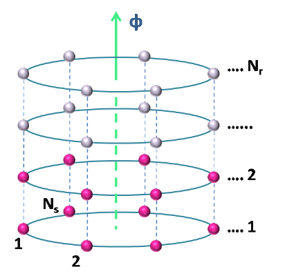
Let us begin with Fig. 1 where a single-wall nanotube subjected to a magnetic flux is shown. The SWNT consists of number of vertically attached co-axial rings where each ring contains lattice sites. In order to get an order-disorder separated nanotube we introduce impurities in one portion which is lower half of the SWNT without disturbing the other half part (i.e., upper half), and, throughout the analysis we follow this prescription for ODS nanotube. For fully disordered nanotube we add impurities uniformly all along the nanotube, and it becomes a conventional disordered one. The perfect nanotube is the trivial one where impurities are no longer introduced and all sites are identical. All these three types of nanotubes can be simulated by a general tight-binding (TB) Hamiltonian pc2 which looks like
| (1) | |||||
where , position of a lattice site, represents th site in the th ring of the SWNT, and, and run from to and , respectively. describes on-site energy which we choose ‘randomly’ from a ‘Box’ distribution function of width (i.e., lies within the range to ) for impurity sites, and this parameter measures the strength of disorder. Whereas, for the perfect atomic sites ’s are same and we set them to zero (viz, for this case ) without loss of generality. and are the intra-and inter-channel nearest-neighbor hopping (NNH) integrals, respectively, and because of the magnetic flux a phase factor () appears into the Hamiltonian when an electron hops along the ring. No such phase factor appears for the hopping from one ring to the other. and are the usual Fermionic operators.
This is all about the TB Hamiltonian of the SWNT. Now to inspect its physical properties first we need to find out allowed energy levels, and for a perfect SWNT we do it completely analytically, while in presence of impurities the eigenvalues are determined by diagonalizing the Hamiltonian matrix of the TB Hamiltonian Eq. 1. For a fully ordered SWNT the energy eigenvalues are expressed as,
| (2) |
where and . Once eigenvalues are found out, the total energy for fixed number of electrons at absolute zero temperature can be obtained by taking the sum of lowest energy levels, and the persistent current is evaluated from the relation pc2
| (3) |
This is the simplest way (viz, the derivative method) of calculating persistent current. Some other approaches are also available skm2 and one can equally utilize anyone of them, but those techniques are normally used for calculating response at different branches of a full system, which is not required for our present analysis.
We investigate conducting properties of SWNT by determining Drude weight which is expressed as kohn ; bouz
| (4) |
where () being the total number of lattice sites in the tube. Finite suggests the conducting phase, while for the insulating phase . The idea of estimating conducting properties by studying Drude weight was originally put forward by Kohn kohn , and latter many other groups have discussed about it in detail sca1 ; sca2 . This is a very good prescription, specially for isolated system (i.e., the system without any external baths).
Finally, to characterize mobility edge phenomenon we calculate inverse participation ratio of different energy eigenstates, and for any particular eigenstate (say) it becomes das2
| (5) |
where ’s are the coefficients. For the localized state IPR is finite and its maximum possible value can be unity, while for an extended state it (IPR) becomes too small and drops to zero in the asymptotic limit das2 .
III Results and discussion
In what follows we present our results. Throughout the analysis we set the intra- and inter-channel NNH integrals at eV and fix the site energy to zero for ordered atomic sites. For disordered regions site energies are random and since they are random we compute the results averaging over a large number of disordered configurations to authenticate all the characteristic features. As the system temperature does not have any significant impact on our present analysis, we fix it at absolute zero, and also set for the entire discussion, for simplification.
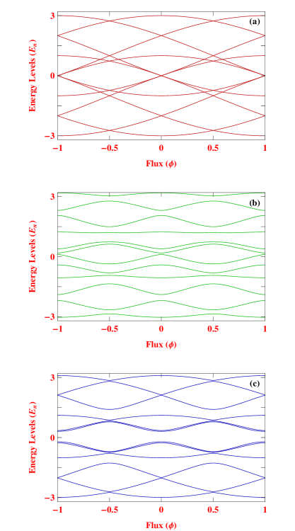
Before addressing the central part i.e., unconventional behavior of circular current and the appearance of phase transition from conducting to insulating zone upon the variation of impurity strength in an ODS SWNT, let us focus on the energy band spectrum and current-flux characteristics for some typical electron fillings of different SWNTs to make the present communication a self-contained one. In Fig. 2 we present the variation of different energy levels with magnetic flux for three different SWNTs, fully ordered, fully disordered and ODS, considering and . From now on we refer energy levels as instead of using two indices (viz, ) to read it quite simply and with this notation no physics will be altered anywhere. From the energy spectra it is observed that the fully ordered SWNT exhibits intersecting energy levels (Fig. 2(a)) where the intersection takes place at integer and/or half-integer multiples of flux-quantum , which may yield a sharp jump in current-flux characteristics at these typical fluxes though it eventually depends on the electron filling. The situation is somewhat different if we introduce impurities. Both for fully disordered and ODS SWNTs all such crossings of energy levels as noticed in fully ordered SWNT completely disappear and energy levels vary continuously with flux (Figs. 2(b) and (c)). At a first glance it is quite difficult to find any difference between the spectra given in Figs. 2(b) and (c), but a careful inspection reveals that for a fully disordered SWNT slopes of the energy levels with flux are lesser than the ODS nanotube, and for some energy levels it is too small, seems almost flat, for which the current will almost vanish. With increasing disorder strength flatness will be more prominent in both these two SWNTs, but for an ODS SWNT we always get some energy levels which exhibit higher slopes which we confirm through our extensive numerics. This definitely gives a hint that for a fully disordered nanotube current gets reduced with , while for an ODS nanotube it may not be the case and from our forthcoming analysis the nature will be clearly understood.
Naturally, a question appears how ground state energy of such different kinds of
SWNTs depends on flux for different electron fillings, since the full spectrum shows many interesting patterns in these cases. To reveal this fact in Fig. 3 we present the dependence of ground state energy as a function of magnetic flux for different band fillings for three different types of SWNTs considering and . Several interesting features are observed associated with filling factor as well as spatial distribution of randomness i.e., whether the tube is partly or fully disordered. For the disordered free SWNT, ground state energy varies smoothly with exhibiting extrema at zero and integer multiples of in the half-filled band case (red curve of Fig. 3(a)). The situation gets changed when the filling factor is less than half-filling, showing a sudden phase change around (see green and blue lines of Fig. 3(a)), establishing a valley-like structure. Quite interestingly we see that the width of this valley region gets increased with decreasing the filling factor. This is the generic feature of such a multi-channel non-interacting system and not observed if we shrink it into a single-channel ring system. This valley-like behavior vanishes as long as impurities are introduced either in the full part or in sub-part of the SWNT (see the spectra given in Figs. 3(b) and (c)).
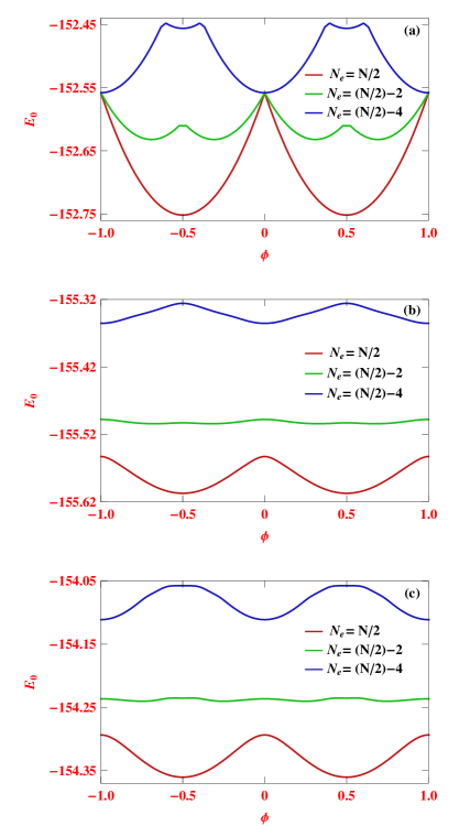
The slope of curve strongly depends on the filling factor for each SWNT, and comparing the curves shown in Figs. 3(b) and (c) it is noticed that for the ODS SWNT change in slope of ground state energy with is quite higher than that of a fully disordered one. Here we present the results for one specific disorder strength (setting ), to set an example, and interesting behaviors are also observed for other disorder strengths. Those characteristics are directly reflected in circular current as discussed below.
Figure 4 displays the variation of circular current as a function of flux for the same set of parameter values as taken in Fig. 3 to get a clear reflectance of energy variation on current. For the fully ordered SWNT current shows saw-tooth like behavior with sharp transitions at integer multiples of when the tube is half-filled. When the filling factor gets reduced additional kink-like structures appear across (green and blue lines of Fig. 4(a)) associated with the valleys in the - curve, and the width of the kinks increases with more reduction of filling factor. Here it is important to note that this kink-like feature is no longer available in a single-channel non-interacting perfect AB ring for any filling factor. With
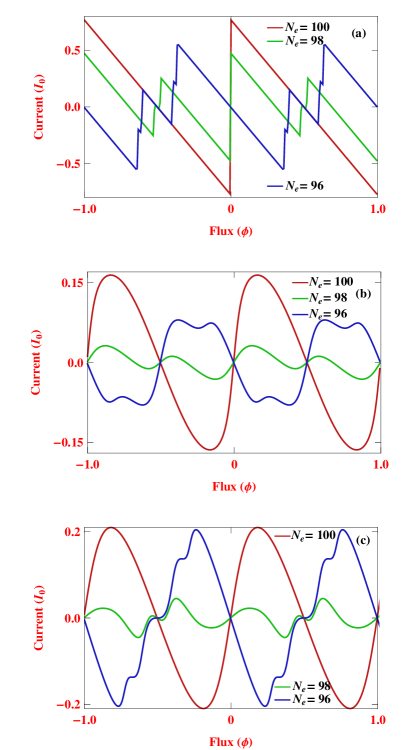
the inclusion of impurities all these kinks disappear (see Figs. 4(b) and (c)) following the - curves. Both the spectra, Figs. 4(b) and (c), exhibit strong dependence of current on which suggests that wide variation of current amplitude can be expected by regulating the filling factor. This is indeed more transparent from the spectrum given in Fig. 4(c), and thus, ODS SWNT will be a very good candidate for regulating current amplitude, or in other words, electrical conductivity that may lead to the useful information in designing switching devices at nano-scale level. The other observation is that for the ODS SWNT current amplitude is comparatively higher than that of the fully disordered one for a specific filling factor. This seems to be expected as for a completely disordered nanotube more scattering takes place rather than the ODS one. It generates an interesting question that can we expect a different behavior in current compared to the conventional spatially uniform disordered system if we increase the disorder strength .
To answer this question let us have a look into the spectra given in
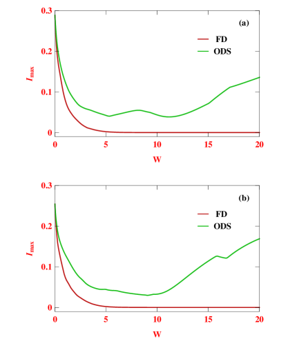
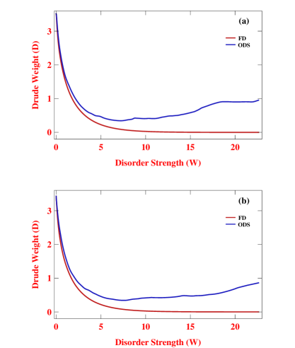
Fig. 5 where the dependence of maximum current amplitude () is shown as a function of for both ODS and fully disordered (FD) SWNTs at two distinct filling factors. corresponds to the maximum absolute current within the flux range zero to one flux-quantum (i.e., one complete period). A completely different scenario is observed between the spatially uniform and non-uniform disordered SWNTs. For the uniform disordered (viz, FD) case, current amplitude gradually decreases with and eventually it drops to zero for large disorder strength. This is quite natural since all the energy eigenstates are getting localized (Anderson type localization) with increasing . On the other hand, for the ODS SWNT initially we get decreasing nature of current like what we get in a uniformly distributed disordered nanotube, but surprisingly the current gets enhanced with the rise of disorder strength (green curves in Fig. 5). And in this strong disorder range current amplitude never decreases even in the limit of large rather it shows increasing tendency, which we confirm through our detailed and comprehensive numerical calculations. At extreme limit it will saturate. Thus we can classify two regions, weak and strong, depending on the strength of for the ODS SWNT where current, and hence, energy eigenstates behave completely differently. In the weak disorder regime usual Anderson type localization is obtained, while for the other regime
anti-localizing behavior is expected with increasing . This phenomenon (anti-localization) can be analyzed from our forthcoming analysis. Before that we want to check how this atypical nature of electronic localization plays the role in electrical conductivity, and we discuss it by studying Drude weight . The results are given in Fig. 6 where two different filled band cases are taken into account. Exactly similar pictures are obtained as described in Fig. 5 which clearly emphasizes that the electrical conductivity can be tuned by regulating the strength of disorder in a spatially non-uniform disordered material. That may give some important inputs towards device technology.
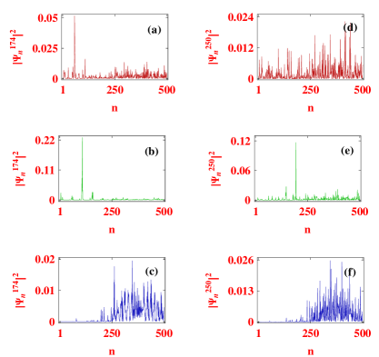
To explain physically the observed atypical nature let us focus on the spectra given in Fig. 7, where we present the probability amplitudes at different lattice sites () of an ODS SWNT choosing arbitrarily two distinct eigenstates, and , for three typical disorder strengths, , and . These three values of are associated with the weak, moderate and strong disorder regimes, respectively. Several interesting features are noticed from the spectra. In the regime of weak disorder, the probability of finding an electron at each lattice site of the -site ODS SWNT is
finite for both the two eigenstates, and it is also true for all other eigenstates, which yields that all the states are extended in nature. Definitely for a perfect SWNT we get more amplitudes at all atomic sites. Now for the typical () where both the current and conductivity are too low (see the blue curves of Figs. 5 and 6), the probability amplitudes drop very close to zero almost for all the atomic sites apart from a single one where it gets a very high value. This is the common signature of a localized state as electron gets pinned at a particular site and does not able to hop along the system. Thus for this very small (not exactly zero, since absolute localization does not take place due to finite size effect) current, and hence, electrical conductivity is obtained. This is the generic feature of Anderson localization ander . The peculiar behavior is obtained when the disorder strength gets increased. For large we clearly see that in the disordered region (lower half of the nanotube i.e., from the sites to where impurities are introduced) probability amplitudes are vanishingly small, whereas large amplitudes are noticed at all sites of the other half of the tube which is impurity free. It indicates that electrons can easily move in this ordered portion of the tube which essentially contributes to finite current. We also observe that the probability amplitudes in these impurity-free sites gradually increase with enhancing the strength of the impurity region. The whole process can be summarized as follows. The ODS SWNT is basically a coupled system where the disordered sector is directly coupled to the ordered one. As disorder favors scattering electrons start to get localized with increasing following Anderson localization ander . Thus more disorder causes more electronic localization and therefore current gradually decreases and reaches to a minimum. So up to typical scattering effect dominates, but beyond this the coupling between the ordered and disordered regions gradually weakens which results suppressing the effect of disorder. Eventually for large disorder these two portions are almost decoupled from each other, as clearly reflected from the probability amplitude spectra given in Fig. 7. The phenomenon of decoupling can also be implemented following the analysis given in Ref. div5 . Thus, when the ordered region is fully detached from the disordered one, electrons move freely in this region without getting scattered resulting a large current, and hence electrical conductivity.
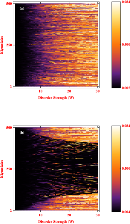
This decoupling effect in the limit of strong disorder enforces the appearance of LTD transition in such ODS SWNT. To implement it we compute inverse participation ratios (IPRs) of different energy eigenstates as a function of . The results are shown in Fig. 8 considering a -site ODS nanotube (Fig. 8(b)) along with the fully disordered one (Fig. 8(a)), for a better comparison between these two different kinds of nanotubes. For the FD nanotube conducting states are available only when the disorder strength is weak, while all these states get localized with increasing . The critical where all the states start to localize decreases with increasing the system size, which justifies the appearance of LTD transition at weak disorder strength satisfying the Anderson prediction in 3D uncorrelated disordered model. Surprising behavior appears for the case of non-uniformly distributed disordered system i.e., ODS SWNT. Even for large we always find the co-existence of localized and extended states. Thus we strongly argue that LTD transition persists in such system irrespective of disorder strength which truly makes the ODS nanotube a special one compared to the FD nanotube.
IV Closing Remarks
To conclude, in the present communication we have shown that a spatially non-uniform disordered material exhibits a completely different behavior of electronic localization compared to a uniformly distributed traditional disordered one. To justify this fact we have made a detailed analysis of magneto-transport properties of non-interacting electrons considering an ODS SWNT along with a fully disordered SWNT. We have essentially characterized the full energy spectra, ground state energy at different band fillings, filling dependent persistent currents and electrical conductivity. Surprisingly we have seen that the ODS SWNT exhibits increasing circular current, and hence, electrical conductivity with the enhancement of impurity strength in the strong disorder regime. This is absolutely in contrast with the spatially uniform traditional disordered material where always decreasing nature with disorder is observed. This anomalous behavior has been clearly validated by inspecting the probability amplitudes at different lattice sites of the ODS SWNT and found that with increasing impurity strength the ordered sector gradually separated from the disordered one which results in suppression of scattering effects and yields higher electrical conductivity. It suggests an opportunity of controlling electron mobility by tuning the doping strength in doped materials. Finally, we have shown that unlike 3D uncorrelated uniform disordered material, the ODS SWNT exhibits mobility edge phenomenon and it persists even at strong disorder. This phenomenon has been clearly justified by investigating inverse participation ratios of different energy eigenstates. Before we end, we would like to state that the present analysis may be useful to analyze conducting properties of several doped materials.
V Acknowledgments
MB and BM would like to thank Physics and Applied Mathematics Unit, Indian Statistical Institute, Kolkata, India for providing some facilities to work.
References
- (1) P. W. Anderson, Phys. Rev. 109, 1492 (1958).
- (2) P. A. Lee and T. V. Ramakrsihnan, Rev. Mod. Phys. 57, 287 (1985), and references therein.
- (3) J.-y. Choi, S. Hild, J. Zeiher, P. Schaub, A. Rubio-Abadal, T. Yefsah, V. Khemani, D. A. Huse, I. Bloch, and C. Gross, Science 352, 1547 (2016).
- (4) S. Sil, S. K. Maiti, and A. Chakrabarti, Phys. Rev. Lett. 101, 076803 (2008).
- (5) S. K. Maiti and A. Nitzan, Phys. Lett. A 377, 1205 (2013).
- (6) S. Aubry and G. Andre, Ann. Isr. Phys. Soc. 3, 133 (1979).
- (7) F. A. B. F. de Moura and M. L. Lyra, Physica A 266, 465 (1999).
- (8) S. Ganeshan, K. San, and S. Das Sarma, Phys. Rev. Lett. 110, 180403 (2013).
- (9) S. Ganeshan, J. H. Pixley, and S. D. Sarma, Phys. Rev. Lett. 114, 146601 (2015).
- (10) Y. E. Kraus, Y. Lahini, Z. Ringel, M. Verbin, and O. Zilberberg, Phys. Rev. Lett. 109, 106402 (2012).
- (11) M. Verbin, O. Zilberberg, Y. E. Kraus, Y. Lahini, and Y. Silberberg, Phys. Rev. Lett 110, 076403 (2013).
- (12) L. Amico, A. Osterloh, and F. Cataliotti, Phys. Rev. Lett. 95, 063201 (2005).
- (13) L. Amico, D. Aghamalyan, F. Auksztol, H. Crepaz, R. Dumke, and L. C. Kwek, Sci. Rep. 4, 4928 (2014).
- (14) L. P. Kouwenhoven, C. M. Marcus, P. L. McEuen, S. Tarucha, R. M. Westervelt, and N. S. Wingreen, in Mesoscopic Electron Transport: Proc. NATO Advanced Study Institutes (NATO Advanced Study Institute, Series E: Applied Sciences) 345, (1997).
- (15) Y. Cui, X. Duan, J. Hu, and C. M. Lieber, J. Phys. Chem. B 104, 5213 (2000).
- (16) J.-Y. Yu, S.-W. Chung, and J. R. Heath, J. Phys. Chem. B 104, 11864 (2000).
- (17) C. Y. Yang, J. W. Ding and N. Xu, Physica B 394, 69 (2007).
- (18) J. X. Zhong and G. M. Stocks, Nano. Lett. 6, 128 (2006).
- (19) J. X. Zhong and G. M. Stocks, Phys. Rev. B 75, 033410 (2007).
- (20) R. Rurali and N. Lorente, Phys. Rev. Lett. 94, 026805 (2005).
- (21) M. Büttiker, Y. Imry, and R. Landauer, Phys. Lett. A 96, 365 (1983).
- (22) H. F. Cheung, Y. Gefen, E. K. Reidel, and W. H. Shih, Phys. Rev. B 37, 6050 (1988).
- (23) A. Schmid, Phys. Rev. Lett. 66, 80 (1991).
- (24) U. Eckern and A. Schmid, Europhys. Lett. 18, 457 (1992).
- (25) H. Bary-Soroker, O. Entin-Wohlman, and Y. Imry, Phys. Rev. B 82, 144202 (2010).
- (26) H. B. Chen and J. W. Ding, Physica B 403, 2015 (2008).
- (27) S. K. Maiti, M. Dey, S. Sil, A. Chakrabarti, and S. N. Karmakar, Europhys. Lett. 95, 57008 (2011).
- (28) S. K. Maiti, J. Comput. Theor. Nanosci. 5, 2135 (2008).
- (29) P. Dutta, S. K. Maiti, and S. N. Karmakar, AIP Conf. Proc. 1536, 581 (2013).
- (30) L. P. Lévy, G. Dolan, J. Dunsmuir, and H. Bouchiat, Phys. Rev. Lett. 64, 2074 (1990).
- (31) V. Chandrasekhar, R. A. Webb, M. J. Brady, M. B. Ketchen, W. J. Gallagher, and A. Kleinsasser, Phys. Rev. Lett. 67, 3578 (1991).
- (32) H. Bluhm, N. C. Koshnick, J. A. Bert, M. E. Huber, and K. A. Moler, Phys. Rev. Lett. 102, 136802 (2009).
- (33) S. K. Maiti, M. Dey, and S. N. Karmakar, Physica E 64, 169 (2014).
- (34) S. K. Maiti, Phys. Status Solidi B 248, 1933 (2011).
- (35) S. K. Maiti, J. Chowdhury, and S. N. Karmakar, J. Phys.: Condens. Matter 18, 5349 (2006).
- (36) W. Kohn, Phys. Rev. 133, A171 (1964).
- (37) G. Bouzerar, D. Poilblanc and G. Montambaux, Phys. Rev. B 49, 8258 (1994).
- (38) S. K. Maiti and A. Chakrabarti, Phys. Rev. B 82, 184201 (2010).
- (39) D. J. Scalapino, R. M. Fye, M. J. Martins, J. Wagner, and W. Hanke, Phys. Rev. B 44, 6909 (1991).
- (40) D. J. Scalapino, S.R. White, and S. Zhang, Phys. Rev. B 47, 7995 (1993).