Analytical study of nano-scale logical operations
Abstract
A complete analytical prescription is given to perform three basic (OR, AND, NOT) and two universal (NAND, NOR) logic gates at nano-scale level using simple tailor made geometries. Two different geometries, ring-like and chain-like, are taken into account where in each case the bridging conductor is coupled to a local atomic site through a dangling bond whose site energy can be controlled by means of external gate electrode. The main idea is that when injecting electron energy matches with site energy of local atomic site transmission probability drops exactly to zero, whereas the junction exhibits finite transmission for other energies. Utilizing this prescription we perform logical operations, and, we strongly believe that the proposed results can be verified in laboratory. Finally, we numerically compute two-terminal transmission probability considering general models and the numerical results matches exactly well with our analytical findings.
I Introduction
Designing of logic gates has always been the subject of intense research since these are considered as the basic building blocks of digital electronics. Among the widespread applications, logic gates carry the electronic information in a traditional computer system where around million gates are embedded to execute computational operations and these gates are made from field-effect transistors (FETs) and metal oxide semiconductor field effect transistors (MOSFETs).
The rapid progress of epitaxial and lithographic techniques has allowed us to fabricate phase-coherence-preserving samples where quantum interference effects could be observed ref1 . Various novel electronic devices such as directional coupler, quantum stub transistor, electron Y-branch switch, and to name a few have been proposed and analyzed ref2 ; ref3 ; ref4 . These devices differ from ordinary electronic gadgets, as they are based on the quantum nature of electrons. More precisely, they rely on ballistic, non-phase-destroying carrier transport, with the advantage of potentially gaining a speed increase of several orders of magnitude without dissipation. Exploiting the effect of quantum interference oj1 ; oj2 ; oj3 ; wal ; int1 ; int2 one can construct logic gates using a device of atomic dimension. Following the pioneering work of de Silva and his group ref5 the idea of designing molecular logic gates ref6 ; ref7 ; ref8 ; ref9 ; new1 has drawn much attention among researchers over last few decades assuming that the logic gates at nano-scale level exhibit much better performance than the traditional logic gates made from FETs and MOSFETs. However, the main limitation of constructing molecular logic gates is that they have much lower gain as molecular systems have sufficiently low transconductance ref10 . Furthermore, after mounting hybrid molecular devices on a surface to construct complex circuits, surface tunneling leakage currents between the device and interconnects might still affect device performance ref11 .
Several other proposals have also been given for logical operations. For instance, photo-induced logic gates using DNA molecules and other nano structures ref5a ; ref11a , though many controversial issues raised by researchers for its future capabilities in designing optical computers ref11b . For optical logic to be competitive, major breakthroughs in non-linear optical device technology should be required, or probably a change in the nature of computing itself. Other logical operations can also be implemented from quantum mechanical effects through quantum computing which usually diverges from Boolean design ref11c .
To find whether simple tailor made geometries are capable of designing logic gates at nano-scale level, few years back one of the authors of us has suggested the possibilities of getting logical operations using simple quantum rings ref12 ; sm1 ; sm2 ; sm3 . The key component for that model was the magnetic
flux threaded by the ring, and it has to be fixed at half-flux quantum (i.e., , where ). Utilizing the concept of complete destructive interference under symmetric condition at all possible logic gates have been explored. But to confine this magnetic flux in a nano-sized ring unrealistically large magnetic field is required mag1 ; mag2 ; mag3 . This situation can be avoided by considering bigger rings. The crucial role of quantum interference effects (constructive and destructive) to achieve few logical operations using nano-rings has also been discussed in another work ref12a where the ring is coupled to three external leads, instead of two.
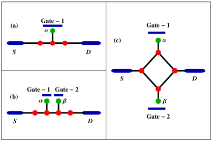
In the present work we intend to establish how logical operations can be achieved in simple two-terminal tailor made geometries without considering any magnetic field, which of course yields an important step along this direction. To do this we consider two different shaped conductors, chain-like and ring-like, and in each case the bridging conductor is coupled to local atomic site(s) through dangling bond(s) (for instance see Fig. 1 where general models of getting logical operations are given. Detailed description of the models with more simplified versions are described in the appropriate places to analyze logical operations). The site energy of any such local atomic site can be altered with the help of an external gate electrode. Assigning two different site energies, associated with two different gate voltages, two states (ON and OFF) of an input signal are defined. Thus, for two-input logic gates we couple two such atoms with the parent conductor. The key idea is that whenever the injecting electron energy matches with site energy of the local atomic site complete suppression of electron transmission is obtained, while finite transmission is available for other cases. This phenomenon can be utilized to perform logical operations, and in the present work we explore all three basic logic gates (OR, AND, NOT) along with two universal gates i.e., NAND and NOR. A complete analytical prescription is given for these logical operations, and finally, we numerically compute the results considering more general models those exactly matches with the analytical findings. We strongly believe that the present proposal can be implemented through an experimental setup in laboratory.
The work is arranged as follows. In Sec. II we present theoretical prescription for a general model. The results are thoroughly analyzed in Sec. III, and finally, we conclude our findings in Sec. IV.
II Theoretical Framework for a general bridge configuration: Transfer Matrix Method
The logical response is described in terms of transmission probabilities in a two-terminal setup. Finite (high) transmission corresponds to the ‘ON’ state of the output, while the ‘OFF’ state represents zero (or vanishingly small) transmission probability. Here, we present the theoretical prescription based on transfer matrix (TM) method tm1 ; tm2 ; tm3 ; tm4 for the calculation of two-terminal transmission probability considering a typical bridge setup, which can easily be utilized in other conducting junctions (those are given in Fig. 1) to explore different logical operations.
Let us begin with Fig. 2 where a one-dimensional (1D) chain is attached to source (S) and drain (D) electrodes through the coupling parameters and , respectively. For non-interacting case one of the most important and usable models for studying electron transport is the nearest-neighbor tight-binding (TB) model. In this framework the TB Hamiltonian of the entire system is given by the sum of three terms: ref16 , where

represents the Hamiltonian of the bridging conductor sandwiched between S and D, and correspond to the Hamiltonians of the electrodes and chain-to-electrode coupling, respectively. These Hamiltonians are written as:
| (1) |
| (2) | |||||
and,
| (3) |
where () corresponds to the creation (annihilation) operator, gives the on-site energy and represents the inter-atomic interaction between the neighboring atomic sites of the wire. () and () represent the creation (annihilation) operators in the source and drain electrodes, respectively, and they are parameterized by site energy and nearest-neighbor hopping integral .
Now we discuss the method of calculating transmission probability for this setup using TM method. Let us start with the Schrödinger equation
| (4) |
where the wave function is expressed in terms of the Wannier functions of different sites as . ’s are the coefficients. In TM approach, the TM essentially connects the wave function of a particular site with its neighboring sites. For an arbitrary site , its wave function (from now on we write as , for simplification) can be linked with the wave functions and of the neighboring sites through the transfer matrix () as
| (5) |
Thus for a -site chain we can write the matrix equation as
| (6) |
where , representing the transfer matrix of the full system, becomes
| (7) |
where, ’s are the transfer matrices for the sites
labeled as , respectively, whereas,
and correspond to the
transfer matrices for the boundary sites at the left and right electrodes,
respectively. Solving Eq. 4 and doing some simple mathematical steps
we get all the transfer matrices and they look like
, ,
, ,
, where .
where is the wave vector. Assuming plane wave incidence with unit
amplitude we can write the wave functions for the source and drain
electrodes as
, for
, for
where and are the reflection and transmission coefficients.
Thus, Eq. 6 can be re-written as
| (8) |
Solving the above equation (Eq. 8) we get the coefficient of transmission probability for each wave vector , associated with incidence energy , and eventually find the transmission probability
| (9) |
This is the general prescription for the calculation of transmission probability through a two-terminal conducting junction. Depending on the bridging system i.e., the conductor sandwiched between two electrodes we only modify the sub-Hamiltonian keeping the rest unchanged.
Since all the logical operations described in the next section are analyzed for very small sized conductors, the average spacing of successive energy levels are considerably large such that moderate temperatures have very minor impact on the proposed analysis. Therefore, we ignore the temperature effect and set it to zero throughout the discussion.
III Results and Discussion
Based on the above theoretical prescription, worked out for a general model, we analytically calculate transmission probabilities of different specific models required to achieve respective logical operations. Below we discuss them one by one. For the case of one-input logic gate (NOT gate) a single atomic site having site energy is coupled with parent lattice via a dangling bond. This coupling is described by the parameter . Whereas two such atoms are considered in the case of two-input logic gates. Their site energies are defined as and , and they are coupled with the identical strength , like one-input gate. The site energies and , treated as the inputs, are controlled by suitable gate electrodes. When no voltage is applied in the electrodes and it is called as the OFF state of the two inputs, whereas in presence of finite gate voltage which is defined as ON state of the inputs. For simplification of analytical calculations we fix all the inter-atomic interactions (, and ) at eV and choose site energies of all the atomic sites apart from local atomic site(s) to zero, though one can choose any other set of parameter values. Only the thing is that the expressions will be quite longer and difficult to read, but the physics will be exactly same. Thus, in the OFF state condition (), site energies of the local atomic sites become identical to the parent lattice sites.
NOT gate: The bridge setup for NOT gate operation is schematically shown in Fig. 3(a) in which the shaded region represents the bridging conductor where a parent site (labeled as ) is coupled to a local site (site number 2) via a dangling bond. The parent site is again directly coupled to the measuring electrodes. To find
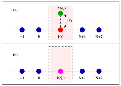
transmission probability for this setup first we write difference equations for these two sites using the Schrödinger equation (Eq. 4) and they are
| (10) |
| (11) |
These equations look very simple as we choose all the inter-atomic interactions at eV and fix site energies of the electrodes and parent lattice sites to zero. Now substituting we get the renormalized difference equation for site as
| (12) |
where the renormalized site energy of site becomes
| (13) |
Thus the setup given in Fig. 3(a) maps exactly to the effective D configuration, (Fig. 3(b)), and therefore, we can utilize the TM method to calculate transmission function . Here we solve Eq. 8 considering with . Doing the necessary steps we eventually reach to the expression of transmission probability as
| (14) |
At a first glance it seems that the energy is dimensionless since transmission probability does not have any dimension. But this is not the case at all. We reach to this relation Eq. 14 only due to the fact that we set all the site energies apart from local atomic site(s) ( and/or ) to zero, and fix the inter-atomic hopping integrals at eV. From the expression Eq. 14 we can clearly explain the NOT gate operation setting the injecting electron energy at eV. When the input is high i.e.,
| Input | Output |
|---|---|
| 0 | 0.75 |
| 1 | 0 |
eV, transmission probability drops exactly to zero (OFF state), while high transmission viz (ON state) is obtained when the input is low (). The response is summarized in Table 1.
In order to check the robustness of our analysis for any such general model
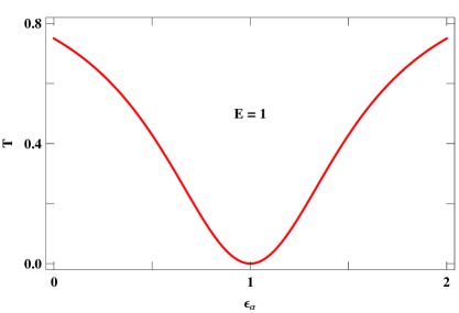
in Fig 4 we plot - characteristics which we calculate numerically for a -site chain considering ( represents the location of the parent atomic site with which the local site is coupled through the dangling bond). Figure 4 clearly describes the NOT gate operation i.e., for eV and when . Thus the numerical results exactly corroborate our analytical findings. In this context it is important to note that one can choose any as the results are independent of this position.
AND and NOR gates: To achieve AND and NOR gates, the setup is slightly modified than the previous one i.e., the configuration used for NOT gate. Using the bridge configuration, given in Fig. 5(a), we can get both AND and NOR operations
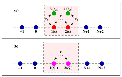
which seems very interesting as only one setup provides two different logical operations. Here two atomic sites, labeled as and , having energies and are connected to the parent sites and respectively. In one step re-normalization the system maps exactly to the D lattice (see Fig. 5(b)) where site energies of atomic sites and get modified as
| (15) |
Under this situation the full transfer matrix becomes
with and . Finally solving Eq. 8 we get the following expression of transmission probability
| (16) |
From this expression we can explain two logical operations (AND and NOR) setting the energy at two different values. For , we get AND operation and the corresponding truth table is given in Table. 2.
| Input-I | Input-II | Output |
| 0 | 0 | 0 |
| 0 | 1 | 0 |
| 1 | 0 | 0 |
| 1 | 1 | 0.75 |
| Input-I | Input-II | Output |
| 0 | 0 | 1 |
| 0 | 1 | 0 |
| 1 | 0 | 0 |
| 1 | 1 | 0 |
Whereas for eV, the NOR operation is obtained and its truth table is shown in Table. 3.
In Fig. 6 we present the density plot of two-terminal transmission probability , computed numerically as functions of and for two different energies
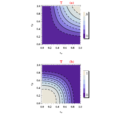
( and eV), for a general model, considering , and . From the spectra it is shown that only when both the two inputs are high the output is high at yielding AND operation (Fig. 6(a)). On the other hand, the same bridge setup exhibits high output only when both the inputs are low under the condition eV resulting the NOR operation (see (Fig. 6(b)). The numerical results completely match with analytical observations.
OR and NAND gates: Finally, we focus on another setup, given in Fig. 7(a), that is used to exhibit OR and NAND operations. Here a diamond like interferometric geometry is taken into account instead
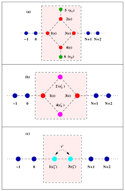
of a chain-like which is connected to two atomic sites having site energies and via two dangling bonds. Here two step re-normalizations are required to get an effective D lattice. In the first step, the effects of th and th atomic sites are incorporated into site numbers and , respectively, to get a regular diamond shaped conductor (see Fig. 7(b)). Under this operation the site energies of these two sites ( and ) become
| (17) |
In the second step re-normalization, diamond shaped conductor moves to a linear one (see Fig. 7(c)) where effectively a bond is formed among the sites and . Both their site energies and inter-atomic hopping integral get modified as,
| (18) |
Once we get this effective linear geometry we can employ method, like previous cases, and the transmission probability becomes,
| (19) |
where . The above expression clearly describes other two logical operations, like
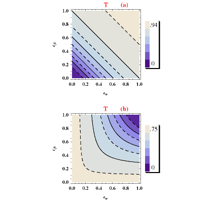
previous setup, by setting injecting electron energy at two distinct values. For we get OR operations, whereas for eV NAND operation is
| Input-I | Input-II | Output |
| 0 | 0 | 0 |
| 0 | 1 | 0.8 |
| 1 | 0 | 0.8 |
| 1 | 1 | 0.94 |
| Input-I | Input-II | Output |
| 0 | 0 | 0.75 |
| 0 | 1 | 0.75 |
| 1 | 0 | 0.75 |
| 1 | 1 | 0 |
At the end, in Fig. 8 we present the density plot of two-terminal transmission probability by varying and to check the sensitivity of logical operations on these quantities. We find that the logical operations are stable for a wide range of parameter values, and thus, can be tested in laboratory.
IV Closing Remarks
In the present work we intend to establish how logical operations can be performed using simple tailor made geometries. Comparing all the propositions we can argue that our proposed model is the most suitable one, particularly due to its simplicity, to design logic gates at nano-scale level. A complete analytical prescription is given to understand three basic (OR, AND, NOT) and two universal (NAND and NOR) logic gates. Two geometrical shapes of the bridging conductor, chain-like and ring-like, are taken into account where in each case the conductor is coupled to a local atomic site or two such sites depending on one input or two input logic gates. By using gate electrode site energy of the local site is controlled which determines the OFF or ON state of an input signal. The key idea is that whenever the site energy of a local atomic site matches with the injecting electron energy, transmission probability drops exactly to zero. This phenomenon is utilized to design the logical operations. In this paper we propose five logical operations and unable to establish other two operations viz, XOR and XNOR gates using such simple setups. Hopefully we will do that in our forthcoming work.
Finally, we would like to state that all these results are valid for a reasonable range of parameter values which we confirm through our extensive numerical analysis and here we present some of them considering more general models with higher number of lattice sites. Thus, we strongly believe that the present proposal can be easily tested in laboratory.
V Acknowledgment
MP would like to thank University Grants Commission, India (F. 2-10/2012(SA-I)) for her research fellowship.
References
- (1) S. Datta, Electronic transport in mesoscopic systems. Cambridge University Press. Cambridge (1999).
- (2) J. A. del Alamo and C. C. Eugster, Appl. Phys. Lett. 56, 78 (1990).
- (3) F. Sols, M. Macucci, U. Ravaioli, and K. Hess, J. Appl. Phys. 66, 3892 (1989).
- (4) T. Palm and L. Thylén, J. Appl. Phys. 60, 237 (1992).
- (5) J. H. Ojeda, C. A. Duque, and D. Laroze, Org. Electron. 41, 369 (2017).
- (6) F. G. Medina, J. H. Ojeda, C. A. Duque, and D. Laroze, Superlattices Microstruct. 87, 89 (2015).
- (7) J. H. Ojeda, R. R. Rey-González, and D. Laroze, J. Appl. Phys. 114, 213702 (2013).
- (8) K. Walczak, Cent. Eur. J. Chem. 2, 524 (2004).
- (9) S. K. Maiti, Phys. Lett. A 366, 114 (2007).
- (10) M. Dey, S. K. Maiti, and S. N. Karmakar, Org. Electron. 12, 1017 (2011).
- (11) A. P. de Silva, H. Q. N. Gunaratne, and C. P. McCoy, Nature 364, 42 (1993).
- (12) F. M. Raymo, Adv. Mater. 14, 401 (2002).
- (13) A. P. de Silva et al. Chem. Rev. 97, 1515 (1997).
- (14) V. Balzani, A. Credi, and M. Venturi, Molecular Devices and Machines (Wiley-VCH, Weinheim, 2003).
- (15) A. P. de Silva and N. D. McClenaghan, Chem. Eur. J. 10, 574 (2004).
- (16) M. Patra and S. K. Maiti, Phys. Lett. A 382, 420 (2018).
- (17) C. Joachim, J. K. Gimzewski, and H. Tang, Phys. Rev. B 58, 16407 (1998).
- (18) F. Ample, I. Duchemin, M. Hliwa and C. Joachim, J. Phys.: Condens. Matter 23, 125303 (2011).
- (19) A. Okamoto, K. Tanaka, and I. Saito, J. Am. Chem. Soc. 126, 9458 (2004).
- (20) Z. Li and G. Li, IEEE Photonics Technol. Lett. 18, 1341 (2006).
- (21) R. S. Tucher, Nature Photonics 4, 405 (2010).
- (22) J. I. Cirac and P. Zoller, Phys. Rev. Letts. 74, 4091 (1995).
- (23) S. K. Maiti, Solid State Commun. 149, 1623 (2009); ibid. 149, 1684 (2009); ibid. 149, 2146 (2009).
- (24) S. K. Maiti, J. Phys. Soc. Jpn. 78, 114602 (2009).
- (25) S. K. Maiti, Phys. Lett. A 373, 4470 (2009).
- (26) S. K. Maiti, J. Comput. Theor. Nanosci. 7, 594 (2010).
- (27) G. Cohen, O. Hod, and E. Rabani, Phys. Rev. B. 76, 235120 (2007).
- (28) D. Rai, O. Hod, and A. Nitzan, J. Phys. Chem. Lett. 2, 2118 (2011).
- (29) D. Rai, O. Hod, and A. Nitzan, Phys. Rev. B 85, 155440 (2012).
- (30) J. Yi and G. Cuniberti, Annals of the NY Academy of Sciences. A three terminal ring interferometer logic gate.
- (31) K. Nakamura, A. Shimizu, M. Koshiba, and K. Hayata, IEEE J. Quant. Electron. 27, 1189 (1991).
- (32) J. Heinrichs, J. Phys.: Condens. Matter 12, 5565 (2000).
- (33) M. Dey, S. K. Maiti, and S. N. Karmakar, Eur. Phys. J. B 80, 105 (2011).
- (34) G. Cordourier-Maruri, R. De-Coss, and V. Gupta, Mod. Phys. Lett. B 25, 1349 (2011).
- (35) M. Patra and S. K. Maiti, Sci. Rep. 7, 43343 (2017).