Logical operations using phenyl ring
Abstract
Exploiting the effects of quantum interference we put forward an idea of designing three primary logic gates, OR, AND and NOT, using a benzene molecule. Under a specific molecule-lead interface geometry, anti-resonant states appear which play the crucial role for AND and NOT operations, while for OR gate no such states are required. Our analysis leads to a possibility of designing logic gates using simple molecular structure which might be significant in the area of molecular electronics.
Organic molecules are considered as the basic building blocks of designing nano-electronic devices r1 ; r2 ; r3 ; r4 ; r5 ; r6 ; r7 ; r8 ; r9 . Especially, the molecules having single or multiple loop geometries are the most promising candidates due to the fact that the effects of quantum interference can be directly implemented in such systems r10 ; r11 ; r12 ; r13 ; r14 ; r15 ; ojeda1 ; ojeda2 ; ojeda3 . Following the idea of Aviram and Ratner r17 , interest in the subject of electron transport through molecular structures has rapidly picked up with considerable theoretical and experimental works r1 ; r2 ; r3 ; r4 ; r5 ; r6 ; r7 ; r8 ; r9 ; r10 ; r11 ; r12 ; r13 ; r14 ; r15 ; r18 ; r19 ; r20 ; r21 ; r22 . Several propositions have been made for designing different molecular based electronic devices like transistor r23 , rectifier r24 , switches r25 ; r25a ; r25b ; r25c , and to name a few. Comparatively much less effort has been given in designing molecular logic gates r26 ; r27 ; r28 ; r29 , particularly, considering simple molecular structures. Here it is important to note that though one of the authors of us has previously suggested the possibilities of designing logic gates using quantum rings but in all those cases large magnetic flux is required new1 ; new2 ; new3 ; new4 and confining a large magnetic flux in a small sized ring has always been a challenging task which we definitely want to avoid if possible.
Motivated by these facts, in the present work, we propose an idea of constructing all three basic logic gates (OR, AND and NOT) considering a benzene molecule exploiting the effects of quantum interference without considering any magnetic flux. For OR and AND gates we use a three-terminal molecular junction, and for NOT gate a two-terminal setup is used. The main idea is that under a particular molecule-to-lead configuration the molecular junction exhibits anti-resonant states ars1 ; ars2 ; r16 at some typical energies. These anti-resonant states, specific to interferometric geometry, play the key role behind AND and NOT operations. For the OR gate operation no such states are required, and thus, can easily be designed. We measure the response in terms of transmission probability. Finite (high) transmission in the output lead represents ‘ON’ state, while ‘OFF’ state means zero (vanishingly small) transmission.
To calculate transmission probability we use Green’s function formalism where the effects of input and output leads are incorporated through self-energy correction r9 . In terms of self-energies the effective Green’s function of the molecule becomes r9 , where is the energy of the injecting electron, is the molecular Hamiltonian and is the self-energy term due to lead-p (p can run from to or to depending on two- or three-terminal bridge set-up). The Hamiltonian is described within a tight-binding (TB) framework and it looks like r14 ; ars1 ; ars2 ; r16 , where and represent the on-site energy and nearest-neighbor hopping (NNH) integral, respectively, and () corresponds to the creation (annihilation) operator for an electron at th site of the molecular ring. Similar kind of TB Hamiltonians are also used to describe the side-attached leads those are parameterized by on-site energy and NNH integral . Once is formed, the two-terminal transmission probability between lead-p and lead-q is determined from the relation r9 , where , and ’s are the coupling matrices due to the coupling of the molecule with lead-p, where the molecule-to-lead coupling is measured by .
In what follows we present our results and discuss the logical operations.

The common set of parameter values which we fix for the numerical calculations are as follows. In the molecule , unless otherwise stated, and eV. In the leads and eV, and the lead-to-molecule coupling is set at eV. Since we focus on the qualitative analysis rather than quantitative one, we choose this set of parameter values. All the physical phenomena remain unchanged for other choices of these parameters.
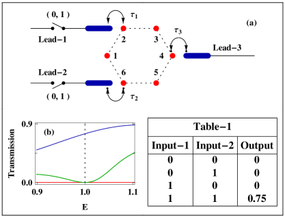
AND Gate: The AND gate operation is summarized in Fig. 1. Figure 1(a) represents the schematic diagram of bridge setup, where each input terminal is connected via a toggle switch which controls the ‘ON’ and ‘OFF’ states of the input signal. In the OFF state electrons are no longer injected into the molecule from the input lead,

and under this situation we assume that the lead is not connected to the molecular ring, and accordingly, we calculate effective Green’s function considering the contributions from the rest leads.
When both inputs are OFF naturally no response is obtained, as shown by the red line of Fig. 1(b). The situation becomes interesting when any one of the two inputs is ON. In the meta connected molecular junction (2-4 or 6-4 connection) anti-resonant states appear at eV. Here we concentrate at eV (we can also take eV, as mentioned at the end of this section, since AND operation is essentially obtained based on the energy location of anti-resonant states), and therefore, we plot the transmission-energy spectrum over a small energy window centering this anti-resonant energy. From the green line of Fig. 1(b) it is clearly seen that () provides a sharp dip (zero transmission) at eV, while it becomes finite at other energies. This feature is associated with such an interferometric geometry ars1 ; ars2 ; r16 ; ars3 and not available in linear-like molecular structure. When both the two inputs are ON, anti-resonant states disappear and the net response (viz, ) becomes high (blue line). Thus, if we think of an experimental setup where electrons having energy eV are injected or only one anti-resonant level having eigenenergy eV is placed within a narrow voltage window (that in principle can be

adjusted by suitable gate electrodes) then a clear AND gate operation is expected at this typical energy (i.e., eV). This is exactly shown in Table 1. An identical AND gate response will also be observed by setting the typical energy eV, since transmission-energy spectrum becomes symmetric around the ring site energy (call it as since ’s are same for all sites of the molecular ring) which is fixed at zero. For identical molecule-to-lead coupling, the anti-resonant states appear at ars1 . Therefore, change of site energy or NNH integral or both simply shifts the whole transmission spectrum along with anti-resonant states, but the AND gate response at these anti-resonant energies remains exactly invariant. Thus, no new physical phenomenon is expected by changing the parameter values.
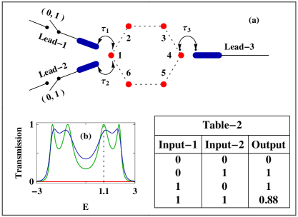
OR Gate: Designing of an OR gate is rather quite simple than any other gate as it does not involve any such anti-resonant states like above. Only thing is that we have to set a typical energy where resonant transmission is obtained when any one or both inputs are high, and definitely it will be the best if we can achieve maximum transmission probability close to unity. The schematic representation of the molecular OR gate is shown in Fig. 2(a) where two inputs are coupled to site and outgoing lead is coupled to site of the molecular ring. The transmission-energy characteristics under different cases of two input signals are presented in Fig. 2(b), where the red, green and blue lines correspond to the identical meaning as prescribed in Fig. 1(b). In a wide range of energy finite transmission is obtained when any one or both inputs are ON, and here we set a specific energy eV to reveal OR operation. The results are summarized in Table 2 under different cases of the input signals which clearly describe the OR gate response.
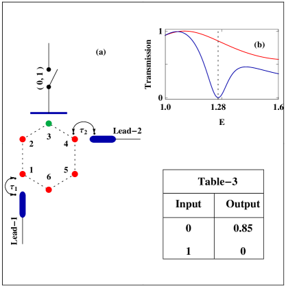
NOT Gate: The molecular setup for designing NOT gate is illustrated in Fig. 3(a), where the benzene molecule is connected to two leads (viz, lead-1 and lead-2) in para configuration. A gate electrode is placed in the vicinity of site which serves as input of the NOT gate and the output response is measured in lead-2. When the input signal is OFF i.e., no gate voltage is applied in the gate electrode, the transmission probability is finite (high) (red line) for the energy window shown in Fig. 3(b). Whereas a sharp dip across eV in transmission curve (blue line) is noticed when the input signal is ON (viz, eV). This is solely associated with the quantum interference effect of electronic waves passing through different arms of the molecular ring. Thus, setting the injecting electron energy at eV the NOT gate operation is clearly visible, and the results are summarized in Table 3.
To conclude, in the present work we address basic three logic operations (OR, AND and NOT) considering a simple molecular structure. The main idea is that the molecular system having a loop geometry exhibits anti-resonant states under a specific lead-to-molecule configuration, and these states are utilized in designing AND and NOT gates. Whereas for OR operation no such anti-resonant states are required and thus easy to operate. We strongly believe that the propositions can be implemented through an experimental setup, and might be significant in the area of present molecular nanotechnology.
MP is grateful to University Grants Commission, India (F. 2-10/2012(SA-I)) for research fellowship.
References
- (1) M. Ratner, Nature 404, 137 (2000).
- (2) A. Nitzan, Annu. Rev. Phys. Chem. 52, 681 (2001).
- (3) C. K. Chiang, C. R. Fincher, Jr., Y. W. Park, A. J. Heeger, H. Shirakawa, E. J. Louis, S. C. Gau, and Alan G. MacDiarmid, Phys. Rev. Lett. 39, 1098 (1977).
- (4) M. Magoga and C. Joachim, Phys. Rev. B 56, 4722 (1997).
- (5) V. J. Langlais, R. R. Schlittler, H. Tang, A. Gourdon, C. Joachim, and J. K. Gimzewski, Phys. Rev. Lett. 83, 2809 (1999).
- (6) J. M. André, J. L. Bredas, B. Themans, and L. Piela, Int. J. Quant. Chem. 23, 1065 (1983).
- (7) G. Rapenne, J. P. Launay, and C. Joachim, J. Phys.: Condens. Matter 18, S1797 (2006).
- (8) C. Joachim, Superlattices Microstruct. 28 305 (2000).
- (9) S. Datta, Electronic transport in mesoscopic systems, Cambridge University Press, Cambridge (1997).
- (10) R. Baer and D. Neuhauser, J. Am. Chem. Soc. 124, 4200 (2002).
- (11) C. Liu, D. Walter, D. Neuhauser, and R. Baer, J. Am. Chem. Soc. 125, 13936 (2003).
- (12) O. Hod, R. Baer, and E. Rabani, J. Phys. Chem. B 108, 14807 (2004).
- (13) O. Hod, R. Baer, and E. Rabani, J. Am. Chem. Soc. 127, 1648 (2005).
- (14) M. Patra and S. K. Maiti, Sci. Rep. 7, 43343 (2017).
- (15) P. Dutta, S. K. Maiti, and S. N. Karmakar, Org. Electron. 11, 1120 (2010).
- (16) F. G. Medina, J. H. Ojeda, C. A. Duque, and D. Laroze, Superlattices Microstruct. 87, 89 (2015).
- (17) J. H. Ojeda, C. A. Duque, and D. Laroze, Org. Electron. 41, 369 (2017).
- (18) J. H. Ojeda, C. A. Duque, and D. Laroze, Physica E 62, 15 (2014).
- (19) A. Aviram and M. Ratner, Chem. Phys. Lett. 29, 277 (1974).
- (20) J. Chen, M. A. Reed, A. M. Rawlett, and J. M. Tour, Science 286, 1550 (1999).
- (21) T. Dadosh, Y. Gordin, R. Krahne, I. Khivrich, D. Mahalu, V. Frydman, J. Sperling, A. Yacoby, and I. Bar-Joseph, Nature 436, 677 (2005).
- (22) C. M. Fischer, M. Burghard, S. Roth, and K. V. Klitzing, Appl. Phys. Lett. 66, 3331 (1995).
- (23) X. D. Cui, A. Primak, X. Zarate, J. Tomfohr, O. F. Sankey, A. L. Moore, T. A. Moore, D. Gust, G. Harris, S. M. Lindsay, Science 294, 571 (2001).
- (24) J. K. Gimzewski and C. Joachim, Science 283, 1683 (1999).
- (25) D. M. Cardamone, C. A. Stafford, and S. Mazumdar, Nano Lett. 6, 2422 (2006).
- (26) C. Guo, K. Wang, E. Zerah-Harush, J. Hamill, B. Wang, Y. Dubi, and B. Xu, Nature Chem. 8, 484 (2016).
- (27) L. Venkataraman, J. E. Klare, C. Nuckolls, M. S. Hybertsen, and M. L. Steigerwald, Nature 442, 904 (2006).
- (28) K. Terabe, T. Hasegawa, T. Nakayama, and M. Aono, Letters to Nature 433, 48 (2005).
- (29) Y. Wada, T. Uda, M. Lutwyche, S. Kondo, and S. Heike J. Appl. Phys. 74, 7321 (1993).
- (30) D. M. Eigler, C. P. Lutz, and W. E. Rudge, Letters to Nature 352 600, (1991).
- (31) A. P. De Silva, H. Q. N. Gunaratne, and C. P. McCoy, Nature 364, 42 (1993).
- (32) Y. Huang, X. Duan, Y. Chi, L. J. Lauhon, K.-H. Kim, and C. M. Lieber, Science 294, 1313 (2001).
- (33) S. Kou et al., Angew. Chem. 120, 886 (2008).
- (34) D. Wang et al., Anal. Chem. 86, 1932 (2014).
- (35) S. K. Maiti, J. Phys. Soc. Jpn. 78, 114602 (2009).
- (36) S. K. Maiti, J. Comput. Theor. Nanosci. 7, 594 (2010).
- (37) S. K. Maiti, Phys. Lett. A 373, 4470 (2009).
- (38) S. K. Maiti, Solid State Commun. 149, 1623 (2009); ibid. 149, 1684 (2009); ibid. 149, 2146 (2009).
- (39) D. rai, O. Hod, and A. Nitzan, J. Phys. Chem. Lett. 2, 2118 (2011).
- (40) K. Walczak, Cent. Eur. J. Chem. 2, 524 (2004).
- (41) M. Dey, S. K. Maiti, and S. N. Karmakar, Org. Electron. 12, 1017 (2011).
- (42) D. rai, O. Hod, and A. Nitzan, J. Phys. Chem. C 114, 20583 (2010).