figure \cftpagenumbersofftable
Optimization of nonhomogeneous indium-gallium-nitride Schottky-barrier thin-film solar cells
Abstract
A two-dimensional model was developed to simulate the optoelectronic characteristics of indium-gallium-nitride (), thin-film, Schottky-barrier solar cells. The solar cells comprise a window, designed to reduce the reflection of incident light, Schottky-barrier and ohmic front electrodes, an -doped wafer, and a metallic periodically corrugated back-reflector (PCBR). The ratio of indium to gallium in the wafer varies periodically throughout the thickness of the absorbing layer of the solar cell. Thus, the resulting wafer’s optical and electrical properties are made to vary periodically. This material nonhomogeneity could be physically achieved by varying the fractional composition of indium and gallium during deposition. Empirical models for indium nitride and gallium nitride were combined using Vegard’s law to determine the optical and electrical constitutive properties of the alloy. The nonhomogeneity of the electrical properties of the aids in the separation of the excited electron–hole pairs, while the periodicities of optical properties and the back-reflector enable the incident light to couple to multiple guided wave modes. The profile of the resulting charge-carrier-generation rate when the solar cell is illuminated by the AM1.5G spectrum was calculated using the rigorous coupled-wave approach. The steady-state drift-diffusion equations were solved using COMSOL, which employs finite-volume methods, to calculate the current density as a function of the voltage. Mid-band Shockley–Read–Hall, Auger, and radiative recombination rates were taken to be the dominant methods of recombination. The model was used to study the effects of the solar-cell geometry and the shape of the periodic material nonhomogeneity on efficiency. The solar-cell efficiency was optimized using the differential evolution algorithm.
keywords:
thin-film solar cell, Schottky barrier, indium gallium nitride (InGaN), periodically corrugated backreflector, optical model, electronic model, nonhomogeneous composition1 Introduction
Alloys of indium gallium nitride () can be tailored to possess a wide range of bandgaps, from 0.70 eV to 3.42 eV, by varying the relative proportions of indium and gallium through the parameter [1]. Pure indium nitride (i.e., ) has a bandgap of eV [2, 3], whereas gallium nitride (i.e., ) has a bandgap of eV. It should be noted that with high indium content (i.e., ) currently suffers from poor electrical characteristics, background -doping due to Fermi pinning above the conduction-band edge [4], and a bandgap that is greater than expected[5, 6]. These problems are exacerbated by -doping of [7].
Solar cells can be designed to use an in-built potential provided by a Schottky-barrier junction, which can occur at a metal/semiconductor interface [8, 9]. By partnering -doped with a metal possessing a large work function —as opposed to, say, employing the more usual -- junction—the problems associated with -doping of the material are avoided. Furthermore, the deposition process is simplified, as only one dopant element is required. Hence, the reduced fabrication costs could offset the lower efficiencies of Schottky-barrier thin-film solar cells.
Theoretical studies [10, 7], which corroborate an earlier experimental study [11], suggest that Schottky-barrier solar cells with relatively high efficiency could be designed. Anderson et al. [12] investigated the efficiency of Schottky-barrier solar cells with periodic variation of the indium-to-gallium ratio. This involved the solution of both the frequency-domain Maxwell postulates in the optical regime and the carrier drift-diffusion equations using the commercial finite-element package COMSOL (V5.2a), in order to simulate the efficiencies of a variety of designs. The efficiency was found to increase significantly on the incorporation of periodic nonhomogeneity with a specific profile.
For the traditional amorphous-silicon ---junction solar cells, the incorporation of a periodically nonhomogeneous intrinsic layer (i.e., layer), along with a metallic periodically corrugated back-reflector (PCBR), can improve overall efficiency by up to 17% [13]. For a Schottky-barrier solar cell made from , the inclusion of these features was shown to increase the total efficiency by up to [12]. In neither case, however, was comprehensive optimization of the design parameters conducted. The improvements seen are likely due to the following reasons:
-
(i)
The excitation of guided wave modes, including surface-plasmon-polariton waves [14, 15, 16] and waveguide modes [17], is made possible by the inclusion of the metallic PCBR [18, 19, 21, 20]. Both types of phenomena intensify the optical electric field inside the photon-absorbing regions of the solar cell, which leads to an increase in the electron-hole-pair generation rate.
- (ii)
- (iii)
The aim of this paper is to expand on the previous work on by providing a comprehensive optimization of the device parameters in order to maximize efficiency. The optical calculations were undertaken using the the rigorous coupled-wave approach (RCWA) [16], while the electrical calculations were undertaken using COMSOL (V5.3a) [26]. Optical absorption could have been maximized if only optical models had been used, but the missing influence of the varying electrical properties would have made optimization of efficiency impossible [13]. For example, if electrical modeling is omitted, the optical absorption can be maximized by minimizing the bandgap, but this would result in a solar cell with a small open-circuit voltage and therefore, quite likely, low efficiency [27].
The plan of this paper is as follows. The design of the chosen solar cell is summarized in Sec. 2.1, with further details available elsewhere[13, 28]. The optical and electrical constitutive properties used in the simulation are presented in Sec. 2.2, while the computational models employed are described in Sec. 2.3. Numerical results are presented in Sec. 3. Closing remarks are presented in Sec. 4.
2 Summary of the two-dimensional (2-D) model
2.1 Solar-cell design
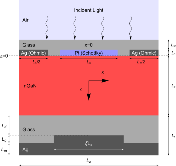
The model is described in detail in Ref. 12. For the sake of completeness, a summary is included here. The simulated Schottky-barrier solar cell is schematically illustrated in Fig. 1. As the solar cell is translationally invariant in the direction, the simulation is reduced to two dimensions (i.e., the plane) without approximation. In the remainder of this paper, the term width refers to the extent along the axis, whereas the term thickness refers to the extent along the axis.
The solar cell comprises a planar antireflection window, a layer containing electrodes, a wafer of , and a layer containing a backreflector. Each of these layers is of uniform thickness. Insolation occurs at normal incidence to the solar cell through the antireflection window, with the wave vector of the incident light aligned with the positive axis.
The device is periodic along the axis with period and has a thickness . The reference unit cell of the device is the region . A planar antireflection window, made from flint glass [29], occupies the region in . The region is occupied by -doped , forming both Schottky-barrier and ohmic junctions with the metal electrodes in the region in . For optical calculations, the ohmic contact and backreflector were assumed to be silver [30], while the Schottky-barrier contact was assumed to be platinum [31]. It must be noted that the electrical properties of silver were not used. The Schottky-barrier electrode, of width , is centered in at along the axis. The two ohmic electrodes, each of width , are centered at in . Note that , and so the electrodes are electrically isolated. It should also be noted that, due to the periodicity of the design, there are an equal number of ohmic and Schottky-barrier electrodes in the solar cell. The gaps between the electrodes, and either or , are occupied by flint glass.
The region in contains both silver and flint glass. The back-reflector is made of two silver slabs welded together. The first slab is optically thick and occupies the region . The second slab occupies the region , where is the duty cycle. Thus, is the corrugation height. The remainder of the region in is occupied by flint glass which electrically insulates silver from .
Absorption of the normally incident solar flux with AM1.5G spectrum [32] was calculated by solving the frequency-domain Maxwell postulates [16]. The semiconductor charge-carrier drift-diffusion equations model the spatial distributions of the electron density and hole density [33, 34]. Because of the nonhomogeneity of the semiconductor (i.e., ), the effective dc electric field acting on
-
(a)
electrons includes a contribution from gradients in the electron affinity, and
-
(b)
holes includes contributions from gradients in both the electron affinity and the bandgap.
Direct, mid-gap Shockley–Read–Hall, and Auger recombination were all included in our simulation. The current density , which is averaged over either the Schottky-barrier electrode (or, identically, both of the ohmic electrodes), was calculated for a range of values of the external biasing voltage .
2.2 Material parameters
For a specific bandgap , the fractional concentration of indium is given by
| (1) |
where the bowing parameter eV [12, 35], and the bandgaps eV and eV.
2.2.1 Optical parameters
The optical refractive index of depends on the free-spaced wavelength and was modeled using two equations. The real part of is provided by the Adachi model as [7]
| (2) |
where and are interpolated from the corresponding parameters for InN and GaN provided in Table 1. The photon energy is denoted by , where m2 kg s-1 is the reduced Planck constant and m s-1 is the speed of light in free space.
2.2.2 Electrical Parameters
The Schottky-barrier work function matched that of platinum in our simulations. Thus, eV.[37] For a specific value of , the electrical properties were modeled using either quadratic or linear (i.e. Vegard’s law [38]) interpolation of data for InN and GaN.
The electron affinity
| (8) |
was modeled using the same quadratic fit as the bandgap, where and are the electron affinities of InN and GaN, respectively. All other parameters presented in the first column of Table 1 were modeled using Vegard’s law of linear interpolation.
Symbol Unit GaN InN Bandgap eV Electron Affinity eV 4.1 5.6 Density of States (Conduction Band) cm-3 Density of States (Valence Band) cm-3 Electron Mobility 1 cm2 V-1 s-1 Electron Mobility 2 cm2 V-1 s-1 Caughey–Thomas Doping Power (Electrons) Caughey–Thomas Critical Doping Density (Electrons) cm-3 Hole Mobility 1 cm2 V-1 s-1 Hole Mobility 2 cm2 V-1 s-1 Caughey–Thomas Doping Power (Holes) Caughey–Thomas Critical Doping Density (Holes) cm-3 Auger Recombination Factor (Electrons) cm6 s-1 Auger Recombination Factor (Holes) cm6 s-1 Direct Recombination Factor cm3 s-1 Slotboom Reference Energy eV Slotboom Reference Concentration cm-3 Conduction-Band Fraction Adachi Refractive-Index Parameter 9.31 13.55 Adachi Refractive-Index Parameter 3.03 2.05
The narrowing of the bandgap associated with doping was incorporated through the Slotboom model [39]. An empirical low-field mobility model—called either the Caughey–Thomas [7] or the Arora [26] mobility model—was used for the variations of the electron mobility and the hole mobility. Details of these models are available elsewhere [12, 7].
The bandgap of was taken to vary periodically in the thickness direction of the solar cell, described by
| (9) |
where is the baseline (maximum) bandgap, is the amplitude, is the period with , is a phase shift, and is a shaping parameter.
2.3 Computational model
The problem of calculating the total efficiency of the solar cell was decoupled into two separate calculations. Firstly, the RCWA[16] was used to calculate the spectrally integrated photon-absorption rate which is ideally equal to the charge-carrier-generation rate. This was then coupled with a 2D finite-element electronic model that was implemented in the COMSOL (V5.3a) software package [26]. In the remainder of this paper, terms in small capitals are COMSOL terms.
2.3.1 Differential evolution algorithm
The differential evolution algorithm (DEA) [40] was used to optimize the solar-cell design. Given parameters in the optimization problem, an initial population of members in the parameter-search space was chosen randomly, with a uniform distribution. After the cost function of the problem had been evaluated at each of these points, the DEA produced a new population of members in the parameter search space to test. This process was iterated until the change in absorptance was less than 1% or until a set amount of time had passed.
By representing the current population as a matrix with each of its columns being vectors in , the next population can be written as
| (10) |
where is the optimal parameter vector found at that stage; is the vector of ’s; is the outer product; and are versions of where the columns have been randomly interchanged; the parameter is the step size to be taken by the DEA at each iteration; and are filter matrices of ’s and ’s generated by the DEA, with having approximately a fraction of ’s, where is termed the crossover fraction; and is the Shur product (elementwise multiplication).
The cost function was taken to be either the efficiency or the optical short-circuit current density . The population number was set to , the crossover fraction was set to , and the step size was set to be randomly distributed in uniformly. Allowing to vary randomly with each iteration has been termed dither, and has been shown to improve convergence for many problems [41].
2.3.2 The RCWA algorithm
Suppose that the face of the solar cell is illuminated by a normally incident plane wave with electric field phasor
| (11) |
As a result of the metallic back-reflector being periodically corrugated, the -dependences of the electric and magnetic field phasors must be represented by Fourier series everywhere as
| (12) | ||||
| and | ||||
| (13) | ||||
where , and as well as are Fourier coefficients. Likewise, the optical permittivity everywhere has to be represented by the Fourier series
| (14) |
where is the permittivity of free space.
Computational tractability requires truncation so that , . Column vectors
| (15) |
and
| (16) |
were set up, the superscript denoting the transpose. Furthermore, the matrixes
| (17) |
and
| (23) |
were set up. The frequency-domain Maxwell curl postulates then yielded the matrix ordinary differential equation
| (24) |
where the -column vector
| (29) |
and the matrix
| (39) | |||||
contains as the permeability of free space, as the null matrix, and as the identity matrix.
The solar cell was discretized along the axis [16]. This effectively broke the domain into a cascade of slices. Each slice was homogeneous along the axis but it was either homogeneous or periodically nonhomogeneous along the axis. Equation (24) was then solved using a stepping algorithm to give an approximation for in each slice. Finally, the Fourier coefficients of the components of the electric and magnetic field phasors were obtained from
| (42) |
Thus, the electric field phasor was determined throughout the solar cell.
The spectrally integrated number of absorbed photons per unit volume per unit time is given by
| (43) |
where is the intrinsic impedance of free space and is the AM1.5G solar spectrum [32]. With the assumption that the absorption of every photon in the layer releases an electron-hole pair, the charge-carrier-generation rate can be calculated as
| (44) |
everywhere in that layer. Whereas nm, is the maximum wavelength that can contribute to the optical short-circuit current density
| (45) |
where (in eV) is the minimum bandgap present in the solar cell and C is the elementary charge.
The integral in Eq. (43) was approximated using the trapezoidal rule [43] with sampling at wavelengths spaced at -nm intervals. The integral in Eq. (45) was also approximated using the trapezoidal rule. The sampling resolution was regular in both directions, with , and .
The optical short-circuit current density provides a rough benchmark for the device efficiency, and is used by many optics researchers who simulate solar cells [42]. However, as recombination is neglected, is necessarily larger than the actually attainable short-circuit current density , which is the electronically simulated current density that flows when the solar cell is illuminated and no external bias is applied (i.e., when ). For the results presented here, calculating only would have been inadequate as the electrical constitutive properties were also significantly varied.
2.3.3 Adaptive- implementation
The calculated value of varies with . An adaptive method was implemented to estimate when is sufficiently large. Equation (43) was evaluated using the trapezoidal rule [43]. At the first value of sampled, , was calculated with and . If the magnitude of the difference between the two calculated values of was greater than a specified tolerance, then was set equal to and was increased by two. This iterative procedure was continued until was less than the specified tolerance for two subsequent comparisons. A maximum value of was enforced in order to force to the calculation to terminate within a reasonable duration. After a successful calculation, the next value of was selected, and and were chosen for the next calculation, where is the ceiling function.
2.3.4 Solution of drift-diffusion equations
The charge-carrier-generation rate , calculated using the RCWA, was processed using an external Matlab™ code and then used as the input, via User-Defined Generation, for the COMSOL electrical model. Recombination was incorporated via Auger, Direct and Trap-Assisted (Midgap Shockley–Read–Hall) phenomena, using parameters as provided in Table 1.
Due to the symmetry in the simulation, only the right half of the domain (i.e., ) was electrically simulated, with Insulator Interfaces applied down that line of symmetry.
Fermi-Dirac carrier statistics were employed along with a Finite volume (constant shape function) discretisation, as this inherently conserves current throughout the solar cell [26]. COMSOL utilizes a Scharfetter-Gummel upwinding scheme. The Free triangular, Delaunay mesh has a maximum element size of nm. Further details can be found in Ref. 12.
The Semiconductor module of COMSOL was used to calculate the current densities flowing through the ohmic, and therefore also Ideal Schottky, electrodes. A prescribed external voltage was applied between these electrodes. The current density flowing through the Schottky-barrier electrode was modeled using Thermionic currents, with standard Richardson coefficients of A K-2 cm-2, and A K-2 cm-2[7, 26]. By sweeping from 0 V up to a value where drops to zero, the - curve was produced. This enabled calculation of the maximum attainable value of the efficiency .
3 Numerical simulation results
3.1 Optimization Study
| Parameter | Name | Symbol | Value/Range |
|---|---|---|---|
| Device Period | nm | ||
| Thickness of -doped Layer | nm | ||
| Minimum Thickness of Insulation Window | nm | ||
| Corrugation Height | nm | ||
| Corrugation Duty Cycle | [0.01,0.99] | ||
| Minimum Thickness of Metal | nm | ||
| Electrode-Region Thickness | nm | ||
| Ohmic-Electrode Width | nm | ||
| Schottky-barrier Electrode Width | nm | ||
| Antireflection-Window Thickness | nm | ||
| Pre-doping Bandgap | eV | ||
| Bandgap Nonhomogeneity Amplitude | eV | ||
| Bandgap Nonhomogeneity Phase | |||
| Bandgap Nonhomogeneity Shaping Parameter | |||
| Bandgap Nonhomogeneity Ratio |
The defined problem has 15 parameters, shown in Tables 2, all of which influence the charge-carrier-generation rate and the efficiency of the solar cell. The choice of four of these parameters was guided by either physical constraints, or they were found to strongly affect the optical response of the solar cell while affecting the electrical characteristics only indirectly, i.e., by changing the spatial profile of the charge-carrier-generation rate.
-
•
A smaller value of was seen to further increase the number of photons absorbed in the ; however, a minimum value of nm was chosen: (i) to model a solar cell where the electrical insulation of the backreflector is maintained, and (ii) to provide a suitable surface for deposition.
-
•
The effect of the minimum thickness of the metallic layer has been omitted from the results. This is because, given a sufficiently thick silver layer, only a trivial amount of the incident light will be transmitted through the solar cell. With chosen to be more than twice the penetration depth of silver across the majority of the AM1.5G spectrum, changes in solar-cell performance for modest perturbations in from this value are minimal.
-
•
A smaller value of was seen to further increase the number of photons absorbed in the . A minimum value of nm was chosen so the contacts are more physically realistic: thinner contacts would likely suffer from uneven deposition and exhibit increased series resistance.
-
•
A strong peak in efficiency was seen when nm, irrespective of the other parameters. This corresponds to the glass coating acting as a quarter-wavelength antireflection coating.
For all data reported here, the values nm, nm, nm, and nm were fixed.
The remaining 11 parameters were allowed to vary within the following ranges: nm, nm, nm, , nm, nm, eV, eV, , , and . These ranges, along with the chosen values of the optical parameters, are summarized in Table 2.
The maximum obtained efficiency was found at: nm, nm, , , , , , , , eV, and nm. These values were computed after 10 DEA population evolutions, and provide an estimate for the maximum efficiency, as well as allowing the upcoming interpretation of the results. Further iterations would provide greater confidence in the conclusions, at the cost of greater computation time.
3.1.1 Results of Optimization Study
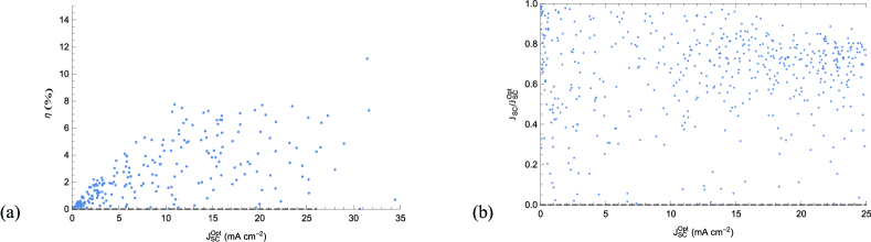
Figure 2 shows plotted against , with each data point corresponding to one DEA population member. The maximum value of was calculated to be mA cm-2, but the maximum efficiency was observed to occur at mA cm-2. Whereas a larger value of increases the likelihood of obtaining a high value of , the former does not predict the latter. Indeed, the designs with values of mA cm-2 produced efficiencies ranging from less than up to over in Fig. 2(a). In part, this is caused by a device with a large optical short-circuit current density not automatically producing a large short-circuit current density . This behavior is shown by the droop at higher values of in Fig. 2(b): as the optical short-circuit current density increases, recombination in the solar cell increases. These observations highlight the importance of conducting full optoelectronic simulations when modeling solar cells, especially when parameters with a strong electrical effect, such as the bandgap, are allowed to vary.
 |
3.1.2 Details of Optimization Study
The results from the optimization study show how the different parameters affect the efficiency of the solar cell. Figures 3 and 4 show the projections of the entire parameter space onto the sets of axes containing the efficiency and each of the optimization parameters. Parameters which have a strong effect on the efficiency have most of their points strongly clustered around the design with the highest efficiency. Each point is colored with the value of .
 |
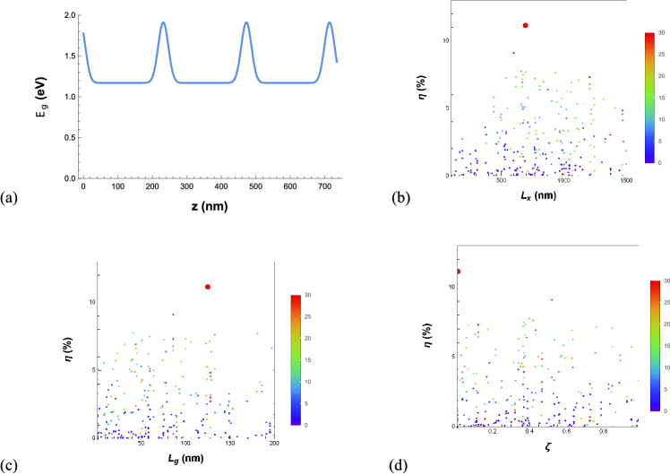
In Fig. 3(a), the thickness of the solar cell is seen to have a moderate effect on the resulting efficiency. The peak visible around nm sees light clustering, with some reasonably efficient solar cells, with , also produced when is less than half the optimal value. Figure 3(b) shows that strongly affects the resulting solar cell efficiency. The peak around eV lie in the region predicted by the Shockley-Queisser limit. Solar cells with narrower bandgaps do produce solar cells with higher optical short-circuit current densities, but the reduction in open-circuit voltage dramatically reduces the efficiency. Figure 3(c) shows that a nonzero amplitude can substantially increase the efficiency. While the structure of the peak is not well resolved, all solar cells with eV had efficiencies less than half that of the maximum attained efficiency. Further increase of beyond eV slowly reduces the attainable efficiency. Figures 3(g) and 3(h) indicate that a small Schottky-barrier electrode and a slightly larger ohmic electrode are required to maximize the efficiency.
A previous study [12] has suggested that optimal values of are integer multiples of , which conclusion is not contradicted by the data; see Fig. 3(d). The strong peak around in Fig. 3(e) is also in line with previous work [13, 12]. At this value of , a wide bandgap is produced in near to the electrodes. This seems of paramount importance for producing high efficiency solar cells with nonhomogeneous bandgaps. The best bandgap profile is shown in Fig. 4(a).
Finally, in Fig. 4, the effects of the PCBR are shown. A period of nm is seen to significantly increase solar cell efficiency. This because the majority of short-wavelength light is absorbed far from the PCBR and so scattering effects are minimal. The grating amplitude and duty cycle are not seen to have strong effects on the solar-cell efficiency—the points do not cluster strongly in Figs. 4(c) and 4(d).
 |
3.2 Detailed study
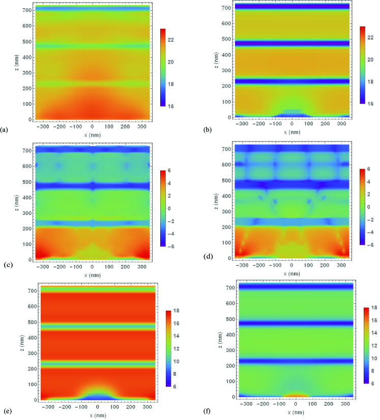 |
The simulated values of the major variables for the highest-efficiency device are shown in Fig. 5. The first two subfigures, (a) and (b), show the generation rate and the recombination rate within the solar cell when the external voltage is zero. Light is incident from below in Fig. 5. The bands of low generation and low recombination at nm correspond to the locations where the bandgap perturation is large, i.e. the bandgap is much wider here. The majority of the photons absorbed in the first nm of the solar cell are collected before recombining, whereas the majority of those absorbed in the rear nm recombine. The exception to this trend are the photons which are absorbed where the bandgap peaks. These are quickly swept out of these regions by the effective electric field produced by the gradient in the bandgap and electron affinity.
Figures 5(c) and 5(d) show the current density produced in the solar cell. By comparing the two figures, it is seen that in the region of the narrow ohmic contact, at the outer edges of the plots, the current density is strongly perpendicular to the contact. The current density in the vicinity of the Schottky barrier, at the center of the plots, is lower, but it is also perpendicular to the contact. The current density towards the back of the solar cell is dramatically lower, supporting the earlier analysis that the majority of the excited carriers in this region recombine.
Figures 5(e) and 5(f) show the electron and hole densities at the short–circuit condition. The electrons are the majority carrier in the majority of the solar cell. In the vicinity of the Schottky-barrier junction, there is a high concentration of holes. In the regions where the bandgap is large, both carrier densities are very low, which has the effect of drastically reducing recombination in these areas. Unfortunately, it also acts to limit current flow across these bands: it may therefore be beneficial in future studies to include lower-bandgap pathways to increase charge-carrier extraction from further back in the solar cell.
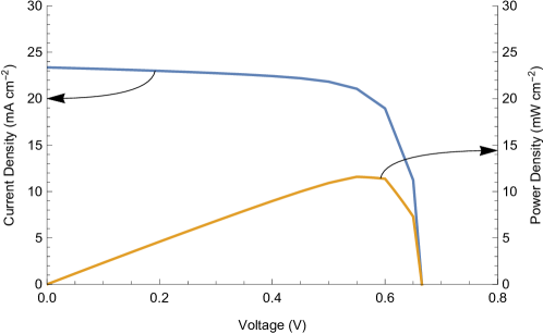
Finally, Fig. 6 shows the resulting JV curve for the optimal device. The short–circuit current is 21.79 mA cm-2, the open–circuit voltage is 0.683 V, and the fill factor is 0.7479.
4 Closing remarks
A combined optoelectronic model was developed to enable to optimization of based Schottky-barrier solar cells. These solar cells possessed a periodically corrugated back-reflector (PCBR), a layer of , metallic electrodes, and an antireflection coating. The optimization was conducted using the Differential Evolution Algorithm. The AM1.5G solar spectrum was used to illuminate the solar cell at normal incidence.
With a solely optical model, it was shown that the optical short–circuit current density of the design is strongly dependent on the thicknesses of the materials that are applied to the surface. A nm thick layer of flint glass acts as a quarter wavelength antireflection coating [44, 45], maximizing . Minimizing the thickness of the front metallic electrodes also maximizes by reducing reflection.
An optimization study, using the differential evolution algorithm and a full optoelectronic model, produced a design for an based Schottky-barrier solar cell with a simulated efficiency of . This design included a periodically nonhomogeneous bandgap, with just over three full periods. The minimum bandgap was eV and the maximum bandgap was eV. The phase of the periodic nonhomogeneity was such that the close to the electrodes has a wide bandgap.
While experimental work is needed to test the veracity of the models employed, it had been shown that based Schottky-barrier solar cells with a high efficiency may be producible if a periodic material nonhomogeneity is included.
Acknowledgements.
This paper is based in part on a paper entitled, “Optimal indium-gallium-nitride Schottky-barrier thin-film solar cells,” presented at the SPIE conference Next Generation Technologies for Solar Energy Conversion VIII, held August 5 to 11, 2017 in San Diego, California, United States [46]. The authors thank F. Ahmad (Pennsylvania State University) for assistance with Figs. 2–5. The research of T.H. Anderson and P.B. Monk is partially supported by the US National Science Foundation under grant number DMS-1619904. The research of A. Lakhtakia is partially supported by the US National Science Foundation under grant number DMS-1619901. A. Lakhtakia also thanks the Charles Godfrey Binder Endowment at the Pennsylvania State University for ongoing support of his research.References
- [1] J. Wu et al., “Superior radiation resistance of InxGaN alloys: Full-solar-spectrum photovoltaic material system,” J. Appl. Phys. 94(10), 6477–6482 (2003).
- [2] J. Wu et al., “Unusual properties of the fundamental band gap of InN,” Appl. Phys. Lett. 80(21), 3967–3969 (2002).
- [3] Y. Saito et al., “Growth temperature dependence of Indium Nitride crystalline quality grown by RF-MBE,” Phys. Status Sol. (b) 234(3), 796–800 (2002).
- [4] S. X. Li et al., “Fermi-level stabilization energy in group III nitrides,” Phys. Rev. B 71(16), 161201 (2005).
- [5] K. Osamura et al., “Fundamental absorption edge in GaN, InN and their alloys,” Solid State Commun. 11(5), 617–621 (1972).
- [6] T. Yodo et al., “Strong band edge luminescence from InN films grown on Si substrates by electron cyclotron resonance-assisted molecular beam epitaxy,” Appl. Phys. Lett. 80(6), 968–970 (2002).
- [7] S. O. S. Hamady, A. Adaine, and N. Fressengeas, “Numerical simulation of InGaN Schottky solar cell,” Mater. Sci. Semicond. Process. 41(1), 219–225 (2016).
- [8] N. K. Swami, S. Srivastava, and H. M. Ghule, “The role of the interfacial layer in Schottky-barrier solar cells,” J. Phys. D: Appl. Phys. 12(5), 765–771 (1979).
- [9] J. P. Colinge and C. A. Colinge, Physics of Semiconductor Devices, Kluwer Academic, New York, NY, USA (2002).
- [10] P. Mahala et al., “Metal/InGaN Schottky junction solar cells: an analytical approach,” Appl. Phys. A 118(4), 1459–1468 (2015).
- [11] J.-J. Xue et al., “Au/Pt/InGaN/GaN heterostructure Schottky prototype solar cell,” Chin. Phys. Lett. 26(9), 098102 (2009).
- [12] T. H. Anderson, T. G. Mackay, and A. Lakhtakia, “Enhanced efficiency of Schottky-barrier solar cell with periodically nonhomogeneous indium gallium nitride layer,” J. Photon. Energy 7(1), 014502 (2017).
- [13] T. H. Anderson et al., “Combined optical-electrical finite-element simulations of thin-film solar cells with homogeneous and nonhomogeneous intrinsic layers,” J. Photon. Energy 6(2), 025502 (2016).
- [14] L. M. Anderson, “Parallel-processing with surface plasmons, a new strategy for converting the broad solar spectrum,” Proc. 16th IEEE Photovoltaic Specialists Conf. 1, 371–377 (1982).
- [15] L. M. Anderson, “Harnessing surface plasmons for solar energy conversion,” Proc. SPIE 408, 172–178 (1983).
- [16] J. A. Polo Jr., T. G. Mackay, and A. Lakhtakia, Electromagnetic Surface Waves: A Modern Perspective, Elsevier, Waltham, MA, USA (2013).
- [17] T. Khaleque and R. Magnusson, “Light management through guided-mode resonances in thin-film silicon solar cells,” J. Nanophoton. 8(1), 083995 (2014).
- [18] P. Sheng, A. N. Bloch, and R. S. Stepleman, “Wavelength-selective absorption enhancement in thin-film solar cells,” Appl. Phys. Lett. 43, 579–581 (1983).
- [19] C. Heine and R. H. Morf, “Submicrometer gratings for solar energy applications,” Appl. Opt. 34, 2476–2482 (1995).
- [20] L. Liu et al., “Experimental excitation of multiple surface-plasmon-polariton waves and waveguide modes in a one-dimensional photonic crystal atop a two-dimensional metal grating,” J. Nanophoton. 9(1), 093593 (2015).
- [21] M. Solano et al., “Optimization of the absorption efficiency of an amorphous-silicon thin-film tandem solar cell backed by a metallic surface-relief grating,” Appl. Opt. 52, 966–979 (2013); erratum: 54, 398–399 (2015).
- [22] F. Ahmad et al., “On optical-absorption peaks in a nonhomogeneous thin-film solar cell with a two-dimensional periodically corrugated metallic backreflector,” J. Nanophoton. 12(1), 016017 (2018).
- [23] M. Faryad and A. Lakhtakia, “Enhancement of light absorption efficiency of amorphous-silicon thin-film tandem solar cell due to multiple surface-plasmon-polariton waves in the near-infrared spectral regime,” Opt. Eng. 52, 087106 (2013); errata: 53, 129801 (2014).
- [24] M. I. Kabir et al. “Amorphous silicon single-junction thin-film solar cell exceeding 10% efficiency by design optimization,” Int. J. Photoenergy 2012(1), 460919 (2012).
- [25] S. M. Iftiquar et al., “Single- and multiple-junction p-i-n type amorphous silicon solar cells with and nc-Si:H films,” in: I. Yun, Ed., Photodiodes – From Fundamentals to Applications, InTech, Rijeka, Croatia (2012); pp. 289–311.
- [26] www.comsol.com/ (20 June 2017).
- [27] B. J. Civiletti et al., “Optimization approach for optical absorption in three-dimensional structures including solar cells,” Opt. Eng. 57(5), 057101 (2018).
- [28] T. H. Anderson et al., “Towards numerical simulation of nonhomogeneous thin-film silicon solar cells,” Proc. SPIE 8981(1), 898115 (2014).
- [29] I. H. Malitson, “Interspecimen comparison of the refractive index of fused silica,” J. Opt. Soc. Am. 55(10), 1205–1208 (1965).
- [30] E. D. Palik (ed.), Handbook of Optical Constants of Solids, Academic Press, Boston, MA, USA (1985).
- [31] W. S. M. Werner, K. Glantschnig, and C. Ambrosch-Draxl, C., “Optical constants and inelastic electron-scattering data for 17 elemental metals,” J. Phys. Chem. Ref. Data 38(4), 1013–1092 (2009).
- [32] National Renewable Energy Laboratory, Reference Solar Spectral Irradiance: Air Mass 1.5 (18 April 2018).
- [33] J. Nelson, The Physics of Solar Cells, Imperial College Press, London, UK (2003).
- [34] S. J. Fonash, Solar Cell Device Physics, 2nd ed., Academic Press, Burlington, MA, USA (2010).
- [35] J. Wu and W. Walukiewicz, “Band gaps of InN and group III nitride alloys,” Superlatt. Microstruct., 34(1), 63–75 (2003).
- [36] G. F. Brown et al., “Finite element simulations of compositionally graded InGaN solar cells,” Solar Energy Mater. Solar Cells, 94(3), 478–483 (2010).
- [37] D. R. Lide (ed.), CRC Handbook of Chemistry and Physics, 89 Ed., CRC Press, Boca Raton, FL, USA (2008).
- [38] L. Vegard. “Die Röntgenstrahlen im Dienste der Erforschung der Materie,” Z. Kristallogr. 67(1-6), 239–259 (1928).
- [39] J. W. Slotboom and H. C. de Graaff, “Measurements of bandgap narrowing in Si bipolar transistors,” Solid-State Electron. 19(10), 857–862 (1976).
- [40] www1.icsi.berkeley.edu/~storn/code.html (6 July 2017)
- [41] S. Das and P. N. Suganthan, “Differential evolution: A survey of the state-of-the-art,” IEEE Trans. Evolutionary Computation 15(1), 4–31 (2011).
- [42] N. Anttu et al., “Absorption and transmission of light in III–V nanowire arrays for tandem solar cell applications,” Nanotechnology 28(20), 205203 (2017).
- [43] Y. Jaluria, Computer Methods for Engineering, Taylor & Francis, Washington, DC, USA (1996).
- [44] D. Chen, “Anti-reflection (AR) coatings made by sol–gel processes: a review,” Solar Energy Mater. Solar Cells 68(3), 313–336 (2001).
- [45] J. Moghal et al., “High-performance, single-layer antireflective optical coatings comprising mesoporous silica nanoparticles,” ACS Appl. Mater. Interfaces 4(2), 854–859 (2012).
- [46] T. H. Anderson, A. Lakhtakia, and P. B. Monk, “Optimal indium-gallium-nitride Schottky-barrier thin-film solar cells,” Proc. SPIE 10368(1), 10368 (2017).
Tom H. Anderson received his M.Sc. from the University of York in 2012, for work on modeling of non-local transport in Tokamak plasmas. He received his Ph.D. from the University of Edinburgh, UK, in 2016 for his thesis entitled Optoelectronic Simulations of Nonhomogeneous Solar Cells. He is presently affiliated with the University of Delaware. His current research interests include optical and electrical modeling of solar cells, numerics, plasma physics, and plasmonics.
Akhlesh Lakhtakia is Evan Pugh University professor and the Charles Godfrey Binder professor of engineering science and mechanics at the Pennsylvania State University. His current research interests include surface multiplasmonics, solar cells, sculptured thin films, mimumes, bioreplication, and forensic science. He has been elected a fellow of OSA, SPIE, IoP, AAAS, APS, IEEE, RSC, and RSA. He received
the 2010 SPIE Technical Achievement Award and the 2016 Walston Chubb Award for Innovation.
Peter B. Monk is a Unidel professor in the Department of Mathematical Sciences at the University of Delaware. He is the author of
Finite Element Methods for Maxwell’s Equations and co-author with F. Cakoni and D. Colton of
The Linear Sampling Method in Inverse Electromagnetic Scattering.