Spin-Orbit Interaction Induced in Graphene by Transition-Metal Dichalcogenides
Abstract
We report a systematic study on strong enhancement of spin-orbit interaction (SOI) in graphene induced by transition-metal dichalcogenides (TMDs). Low temperature magnetotoransport measurements of graphene proximitized to different TMDs (monolayer and bulk WSe2, WS2 and monolayer MoS2) all exhibit weak antilocalization peaks, a signature of strong SOI induced in graphene. The amplitudes of the induced SOI are different for different materials and thickness, and we find that monolayer WSe2 and WS2 can induce much stronger SOI than bulk WSe2, WS2 and monolayer MoS2. The estimated spin-orbit (SO) scattering strength for graphene/monolayer WSe2 and graphene/monolayer WS2 reaches 10 meV whereas for graphene/bulk WSe2, graphene/bulk WS2 and graphene/monolayer MoS2 it is around 1 meV or less. We also discuss the symmetry and type of the induced SOI in detail, especially focusing on the identification of intrinsic (Kane-Mele) and valley-Zeeman (VZ) SOI by determining the dominant spin relaxation mechanism. Our findings pave the way for realizing the quantum spin Hall (QSH) state in graphene.
pacs:
Valid PACS appear here
I Introduction
Two dimensional (2D) layered materials have provoked tremendous interest since the first demonstration of mechanical exfoliation of graphene geim1 . A growing number of recent reports on these materials have revealed that they exhibit many intriguing physical properties, including superconductivitysuper1 ; super2 ; super3 ; super4 , ferromagnetism ferro1 ; ferro2 ; ferro3 , quantum spin Hall (QSH) state qsh1 ; qsh2 ; qsh3 ; qsh4 and Weyl semimetal state weyl1 ; weyl2 ; weyl3 . While these properties in the two dimensional limit are of great interest in themselves, one can also exploit them as building blocks to generate novel phenomena through interface interactions between two different materials geim2 .
Among the many intriguing phenomena realized via interface interactions, inducing spin-orbit interaction (SOI) in graphene is particularly attractive for application to spintronics manuel and topological physics kane1 ; kane2 . So far many works have reported both theoretically and experimentally that strong SOI can be induced in graphene extrinsically by hydrogenation balakrishnan ; gmitra1 ; castroneto , adatom deposition adatom1 ; wu ; balakrishnan2 and intercalation of heavy atoms between graphene and metallic substrates in chemical vapor deposition (CVD)-grown graphene adatom2 ; adatom3 ; adatom4 ; gold . On the other hand recent works have focused on graphene/transition-metal dichalcogenides (TMDs) heterostructures as a platform. TMDs are 2D materials like graphene, but their SOI is much larger than that of graphene owing to the heavy transition metals xiao . This method is more advantageous than the previous ones since it preserves the quality of graphene. Recent theoretical and experimental studies revealed that graphene proximitized by TMD can acquire strong SOI through interfacial coupling avsar2 ; wang ; wang2 ; yang ; yang2 ; gmitra2 ; gmitra3 ; roche ; cysne ; offdani ; ilic ; Alsharari ; valenzuera ; vanwees ; frank ; zihlmann ; wakamura ; eroms1 ; eroms2 . Experimentally, the induced SOI is estimated through transport measurements of nonlocal voltages induced by spin currents or weak antilocalization (WAL) measurements at low temperatures, exhibiting strongly enhanced spin-orbit scattering in graphene. However, estimates of the induced SOI are not in good agreement with the theoretically calculated values based on ab initio calculations, and there are sometimes one order of magnitude differences between them.
Beyond the amplitudes, the symmetry of the induced SOI is important. Indeed, the QSH state is one of the intriguing states expected to emerge if strong enough SOI is induced in graphene. It requires symmetric SOI, where the axis is normal to the graphene plane kane1 ; kane2 . For pristine graphene this symmetric SOI is provided by intrinsic (Kane-Mele (KM)) SOI. On the other hand asymmetric SOI is also expected in realistic experimental situations, induced by Rashba SOI due to the inversion symmetry breaking by the substrate or perpendicular electric fields.
Recent theoretical studies propose the existence of a new type of SOI in graphene/TMD systems: a valley-Zeeman (VZ) SOI induced in graphene due to the broken sublattice symmetry roche ; zihlmann . This SOI provokes the spin splitting of degenerate bands, with out-of-plane spin polarization at and points, and an opposite spin-splitting in different valleys. Analogous to the Zeeman-splitting, the SOI is named VZ SOI because the effective Zeeman fields are valley-dependent. This is the dominant SOI in TMDs, and it is also predicted to be induced in graphene on TMD roche . One of the important consequences of the VZ SOI is the anisotropic spin relaxation, as revealed by recent first principle calculation and experimental studies roche ; zihlmann ; valenzuera ; vanwees . In terms of symmetry the VZ SOI is symmetric, and it is predicted to yield topologically-unprotected edge states frank .
In this paper, we present a systematic study of SOI induced in graphene/TMD heterostructures. We measure magnetoresistance at low temperatures and demonstrate that strong SOI is induced in graphene by all investigated TMD crystals: monolayers of WSe2, WS2 and MoS2, as well as bulk WSe2 and WS2. We observe a clear difference between monolayer and bulk TMDs in the capacity to induce strong SOI in graphene as reported before wakamura . For both WSe2 and WS2, the induced SOI is stronger when the TMD is monolayer than bulk. Monolayer WSe2 and WS2 induce comparable amplitudes of SOI, whereas monolayer MoS2 generates much smaller SOI. For all samples with different TMDs, we find that the symmetric SOI is dominant. To identify the type of symmetric SOI, we elucidate the spin relaxation mechanism by plotting the relation between the momentum relaxation time and the spin-orbit time . The dominant Elliot-Yafet (EY) mechanism around the Dirac point indicates the importance of KM SOI in this low doping region. We also discuss the possibility of VZ SOI and the reason for the suppressed Rashba SOI, taking into account recent reports on band structures of graphene/TMD systems measured by angle-resolved photoemission spectroscopy (ARPES) arpes1 ; arpes2 ; arpes3 and scanning tunneling microscopy (STM) studies on Moiré patterns moire1 ; moire2 ; moire3 .
II Weak Antilocalization in graphene
We exploit weak (anti)localization measurements to estimate the SOI induced in graphene by TMDs. At low temperatures, large coherence length of electrons causes quantum interference between time-reversed pairs of closed trajectories of electron wave packets, leading to weak localization (WL) of electrons bergmann . When SOI is sufficiently strong, the spin of the electrons rotates during a closed loop, leading to an additional phase difference between the time-reversed pairs of the electron wave packets. This results in antilocalization of electrons (WAL effect). An external magnetic field breaks time-reversal symmetry, and as a result when WL (WAL) is dominant the resistance decreases (increases) with an increasing magnetic field. Thus magnetoresistance measurements allow to identify the regime (WL or WAL) to which the system belongs, and provide an estimate of the SOI amplitude.
Dirac fermions in graphene are known to be robust against disorder due to the chiral nature of valley-conserving transport ando . However, short range elastic scattering gives rise to intervalley scattering. When the intervalley scattering rate is large compared to the dephasing rate (), WL1 ; WL2 localization of Dirac fermions in graphene is restored. Many experimental studies have shown evidences of weak localization at low temperatures where WL1 ; WL2 ; WL3 ; WL4 . In this regime, if graphene acquires strong SOI it is therefore possible to observe weak antilocalization (WAL) effects due to the real spin-orbit coupling rather than the pseudospin-orbit coupling Tikhonenko . The theoretical formula for the magnetoconductivity correction in the WAL regime for is written as mccann
| (1) |
where , with the digamma function, , where sym (asy) denotes the symmetric (asymmetric) contribution to the SOI (discussed below in detail) and with the diffusion coefficient. Fits of this formula to the experimental magnetoconductance curves provide three parameters , and . determines the total amplitude of SOI in the system, and the () term is associated with symmetric (asymmetric) SOI. In the case of graphene on TMD, symmetric SOI includes KM and VZ SOI, and the asymmetric SOI is attributed to Rashba or pseudospin inversion asymmetry (PIA) SOI. Details of these different types of SOI will be discussed in a later section. As predicted in the original papers by Kane and Mele kane1 ; kane2 , to induce the QSH state, dominant KM SOI and small Rashba SOI are required to conserve as a well-defined quantum number. Therefore, if other types of SOI are not considered (e.g. VZ SOI), the ratio between and is a key factor to determine the possibility to realize the QSH state in the system.
| Sample | Mobility [cm2V-1s-1] | Size [m m] |
|---|---|---|
| Mono WSe2 | 21000 | 68 |
| Mono WS2 A | 12000 | 612 |
| Mono WS2 B | 7000 | 56 |
| Mono MoS2 A | 4700 | 612 |
| Mono MoS2 B | 1850 | 78 |
| Bulk WSe2 | 21600 | 57 |
| Bulk WS2 A | 9000 | 58 |
| Bulk WS2 B | 7000 | 55 |
III Sample Preparation and Measurement Details
Graphene for all heterostructures is prepared by mechanical exfoliation of natural graphite on SiO2(285 nm thickness)/doped-Si substrates. Monolayer graphene is identified by means of optical contrast under the microscope, and by quantum Hall effect measurements. For TMDs, the fabrication process is different for different materials: Monolayer WS2 and MoS2 are prepared by the CVD method wakamura ; arpes2 ; arpes3 ; reale , and the other TMDs are prepared by mechanical exfoliation of bulk cristals on SiO2/doped-Si substrates. For graphene/monolayer TMD samples, graphene is transferred on a monolayer TMD by using polymethyl methacrylate (PMMA) or mechanically exfoliated hexagonal boron-nitride (hBN) using polydimethylsiloxane (PDMS). For graphene/bulk TMD samples, a bulk TMD is deposited on graphene. Conventional electron beam lithography techniques are employed to fabricate electrical contacts, and 5 nm Ti and 100 nm Au are subsequently deposited by electron gun evaporation. Measurements are performed in a dilution refrigerator employing a conventional lock-in technique with an excitation current of = 10 nA and 77 Hz unless otherwise noted. In the following sections, for simplicity graphene/monolayer TMD structures are termed Mono MX2 (M= W or Mo, X= S or Se) and graphene/bulk ones Bulk MX2. In Table 1 we give the geometry and mobility of all investigated samples.
IV Experimental Results
We evaluate the SOI induced in graphene on various TMDs by means of magnetotransport measurements at sufficiently low temperatures, where the WAL due to the chirality of graphene is negligible because Tikhonenko . This point will be discussed further in the section VC. To obtain clear weak (anti)localization peaks, we average over 50 curves with different in a 10 V window. This is because the height of the peaks is of the order of , the same order of magnitude as universal conductance fluctuations (UCFs) since the sample size is comparable to the phase coherence length. In the following subsections we show the experimental results of the magnetotransport measurements for each graphene/TMD heterostructure. In the WAL data we obtain the magnetoconductivity correction () by converting the original data of two-terminal resistance () with subtraction of contact resistance and taking into account the aspect-ratio of the device.
IV.1 Graphene/WSe2 structures
In this subsection we show the experimental results obtained from Mono WSe2 and Bulk WSe2. WSe2 has the largest intrinsic SOI among TMDs both in the valence band and conduction band xiao ; kosmider ; burkard .
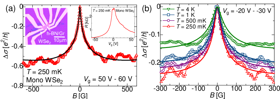
We first discuss the results for Mono WSe2. The inset of Fig. 1(a) shows the gate voltage () dependence of the resistance at 250 mK for Mono WSe2gmitra3 , and the optical microscope image of the device. The resistance exhibits slight asymmetry in , and an anomalous saturation is observed around the Dirac point. The origin of this plateau is still unclear. We note that the resistivity of the monolayer WSe2 is much larger than that of graphene, thus the charge transport is dominated by graphene, as evidenced by the curve that is typical of graphene. The calculated mobility from the inset of Fig. 1(a) is 21000 cm2V-1s-1. This mobility is higher than that of our previous study of graphene on WS2 wakamura but lower than other reports zihlmann ; eroms1
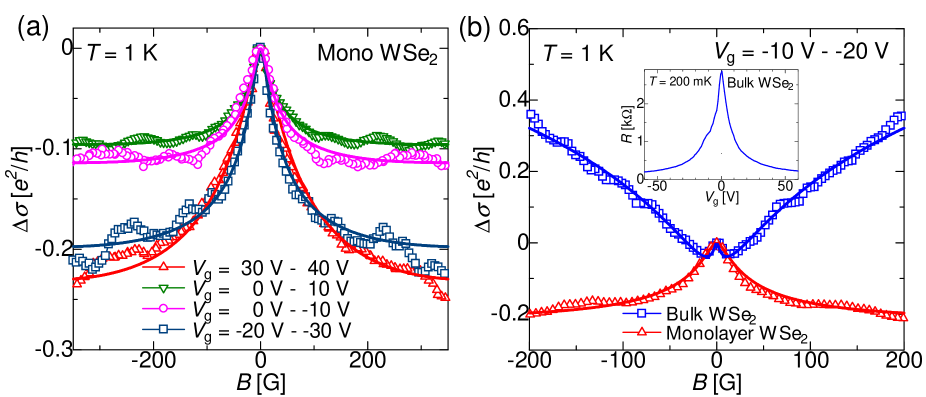
Figures 1(a) and (b) show the conductivity correction () as a function of the magnetic field () applied perpendicular to the graphene plane, in the window of specified in the figure. For all temperatures between 250 mK and 4 K, exhibits WAL with a clear peak at = 0, indicating strong SOI induced in graphene. Similar peaks are observed for all the gate voltage ranges between 60 V and 60 V. In Fig. 2(a) we compare representative curves for different gate voltage ranges. The curves have a similar shape for the electron-doped and hole-doped region.
It is interesting that outside the central peaks, all curves are flat with increasing . As pointed out in the previous studies wakamura ; bergmann ; roche2 , the flat tails in high regions are a signature of strong induced SOI, as will be discussed further below.
We next discuss the experimental results obtained from Bulk WSe2. Previous studies have pointed out striking differences in electrical and optical properties between monolayer and bulk TMDs, and among them the different band structures are especially influential for transport properties klein ; rama ; terrones . To compare the induced SOI in graphene on monolayer and bulk WSe2, we therefore measure the magnetoresistance of graphene on bulk WSe2. We here show the data of the sample with the mobility of 21600 cm2V-1s-1, similar to that of Mono WSe2 sample discussed above. The Dirac point of Bulk WSe2 is located at = 0, just as for Mono WSe2. Figure 2(b) displays the comparison of the curves taken for Mono WSe2 and Bulk WSe2 for the same gate voltage range. The shapes of the two curves are clearly different, and that from Bulk WSe2 displays a striking upturn in the high B region, which contrasts with the flat or slightly downward sloping magnetoconductance of Mono WSe2. As discussed in the next section, this upturn is the signature of moderate SOI induced in graphene, smaller than induced by monolayer WSe2 and WS2. Similar shape differences are also observed for other gate voltage regions.
IV.2 Graphene/WS2 structures
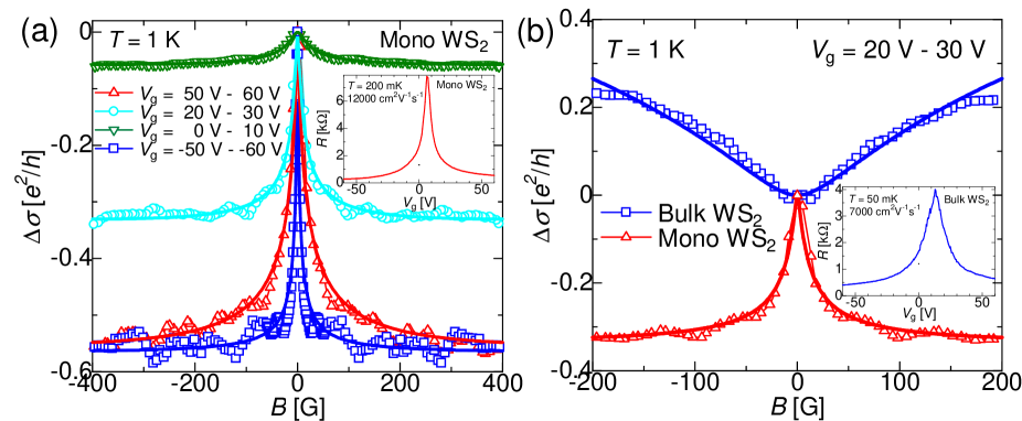
Since we have already reported strong SOI induced in the graphene/WS2 structures in our previous paper wakamura , we here briefly provide an overview of the results obtained from the graphene/monolayer WS2 (Mono WS2) and graphene/bulk WS2 (Bulk WS2) samples, using data not shown in our previous paper wakamura . Figure 3(a) shows from one of the Mono WS2 samples for four different gate voltage ranges. The mobility of this sample is 12000 cm2V-1s-1. For all gate voltage ranges, including close to the Dirac point, we observed WAL, a signature of the strong SOI induced in graphene by monolayer WS2. In contrast to Mono WSe2, the shape of is electron-hole asymmetric in Mono WS2. We note that for the data with between 50 V and 60 V (shown in Fig. 3(a)) a temperature-independent background signal is subtracted from the original data (see the discussions below). We also carried out low-temperature magnetotransport measurements for Bulk WS2, and one curve is compared with that of Mono WS2. The mobility of the sample is 7000 cm2V-1s-1. As demonstrated for the graphene/WSe2 heterostructure, there is a striking difference in the shape of the curves between Mono and Bulk WS2. The smaller peak around = 0 and strong upturn for higher region for the Bulk WS2 samples indicate that the induced SOI is smaller for Bulk WS2 than for Mono WS2.
IV.3 Graphene/MoS2 structures
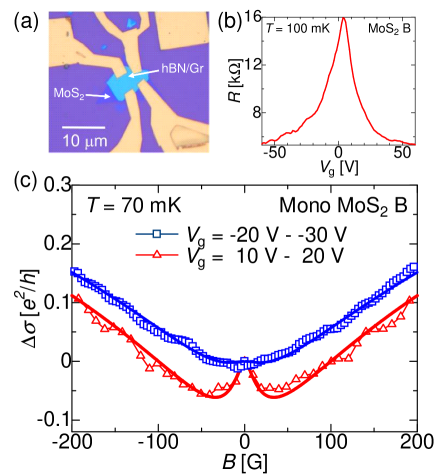
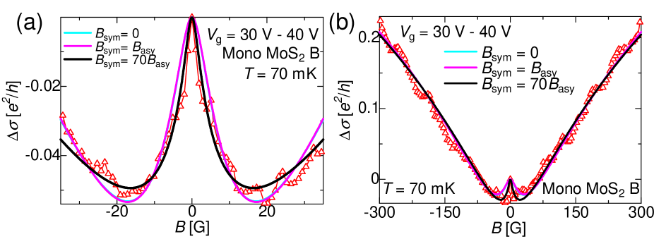
To explore the difference in the induced SOI on graphene from different TMDs, we also investigated SOI of graphene in proximity to MoS2. MoS2 has intrinsic SOI smaller than WSe2 and WS2. The calculated intrinsic spin-orbit splittings for the valence bands are 150 meV, 430 meV and 460 meV for MoS2, WS2 and WSe2, respectively xiao . Therefore if the SOI induced in graphene is provided by interface interactions with TMD, MoS2 should induce smaller SOI in graphene than graphene/WSe2 (or WS2) structures. Based on this assumption we conducted low temperature magnetoresistance measurements on graphene on monolayer MoS2 (Mono MoS2) samples. Figure 4(c) displays a curve for one of the Mono MoS2 samples. The WAL peak is observed around = 0 as for other graphene/TMD structures. However, in contrast to Mono WSe2 and WS2, strongly increases for higher region, and similar characteristics are observed for other gate voltage ranges. This reveals that the SOI induced in graphene by monolayer MoS2 is smaller than that for Mono WSe2 and WS2 samples, and the amplitudes are similar to those of Bulk WSe2 and WS2. Another sample of graphene/monolayer MoS2 with larger graphene mobility also yields comparably small induced SOI. In Fig. 5 we show for Mono MoS2 B in small field region (Fig. 5(a)) and in high field region (Fig. 5(b)). For the graphene/MoS2 devices, it is essential to evaluate the amplitudes of SOI in small field region as discussed below.
V Analysis
V.1 Subtraction of the background signals
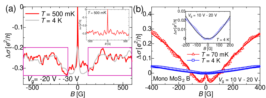
As discussed in previous studies wang2 ; zihlmann ; wakamura , WAL signals are sometimes superimposed a top of temperature-independent magnetoresistance backgrounds particularly for high regions wang2 ; zihlmann which need to be subtracted for a proper analysis of WL and WAL signals. In previous studies zihlmann this background was sometimes attributed to a classical magnetoresistance contribution proportional to , but this temperature-independent component in our case has a different shape. Although the origin of these signals is still unclear, the temperature independence indicates that they stem from classical contributions rather than quantum contributions. Since the theoretical formula used to fit the experimental results considers only quantum contributions, it is justified to subtract these temperature independent components from the original signal. We note that this subtraction dramatically changes the estimation of the induced SOI as pointed out in previous reports wang2 ; roche2 ; grbic . For Mono WS2, a temperature independent part is observed particularly for 0. By contrast, the existence of a temperature independent magnetoconductance background in Mono WSe2 only appears for some gate voltage ranges in both electron-doped and hole-doped regions.
In Fig. 6(a) we show the original data of from Mono WS2 taken at 500 mK and at 4 K. at 500 mK after the subtraction of the temperature independent magnetoresistive component is displayed in the inset. Note that at 4 K is shifted vertically so that the temperature independent part overlaps with that at 500 mK. One can clearly see that for 100 G, is the same at 500 mK and 4 K except for the strong conductance fluctuations observed at 500 mK. Keeping the original data points for 100 G, we subtract the shifted at 4 K from the original at 500 mK, namely, (, 500 mK, subtracted) = (, 500 mK, original) - (, 4 K, shifted). After subtraction, the curve is flat for high field regions. The subtraction of background signals is performed for Mono WSe2 and WS2 for certain ranges of gate voltage , but not for the other samples. For example, Mono MoS2 exhibits a temperature dependent upturn, as shown in Fig. 6(b) which is included in the analysis of the quantum conductivity correction.
V.2 Analysis of the weak antilocalization signals to evaluate SOI
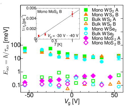
Based on the above considerations, we attempt to fit the experimental results using the equation (1) for the weak antilocalization. We first discuss the total amplitudes of the SOI determined by . In Fig. 7 we plot the spin-orbit scattering strength defined as for each system as a function of the gate voltage. These systems can be divided into two groups, one that exhibits strong spin-orbit scattering ( 10 meV) and the other that shows moderate spin-orbit scattering ( 1 meV). Clearly, Mono WSe2 and the two Mono WS2 samples belong to the former group and yield strong that amounts to 10 meV or even larger. In contrast, for Bulk WSe2 and Bulk WS2 are in the latter group and is more than an order of magnitude smaller. This striking difference between graphene/monolayer TMD and graphene/bulk TMD is consistent with our previous study wakamura . On the other hand, the two Mono MoS2 samples exhibit 1 meV, similar to Bulk WSe2 and Bulk WS2. Therefore the amplitudes of the induced SOI depends not only on the thickness of the TMD layer but also on the type of TMD. As briefly discussed in the previous section, given that the intrinsic SOI of monolayer MoS2 is three times smaller than that of monolayer WSe2 and WS2, it is reasonable that the induced SOI in graphene is smaller for the graphene/MoS2 system. We note that for the samples with strong SOI (Mono WS2 and Mono WSe2), the estimated is close to the momentum relaxation time and for some gate voltage ranges it is even smaller (). Since this limit is out of the validity range of formula (1), in the discussion (on the spin relaxation mechanism) below we exclude the data points in this limit.
V.3 Effect of intervalley scattering
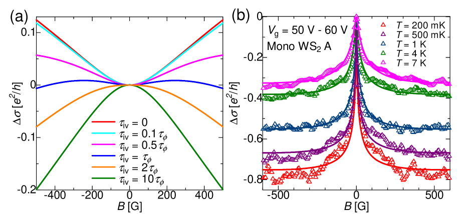
For all of the fits we have assumed that . By doing so, we extract parameters which are consistent for all samples investigated in a wide range of gate voltages and temperatures. On the other hand, a recent theoretical study has proposed that the WAL peaks observed in our experiments without upturn in high fields could be reproduced in the limit ilic . In this limit weak antilocalization can be driven by the chirality Tikhonenko , if the induced SOI is small. To clarify the effect of intervalley scatterings on in high field region, we plot calculated curves where SOI is small and the ratio between and determines the shape of . In this case can be expressed as mccann2
| (2) |
where we neglect the contribution from intravalley scatterings for simplicity. In Fig. 8(a) we show the simulated curves with different ratio between and . In the limit of , the shape of is insensitive to the change of the ratio /. However, when , exhibits a crossover from upturn to downturn feature, and is highly sensitive to the change of /. It is important to note that our samples with the strong induced SOI (Mono WSe2 and Mono WS2) show flat tails in the high field region over a broad range of temperature (between 250 mK to 7 K, see Fig. 8(b) as an example). Because is independent of tempearture and varies dramatically in this range of temperature (see the inset of Fig. 7 and Fig. 9), the ratio / also changes a lot. Therefore the flat tails observed in the broad range of temperature can only be explained in the limit .
V.4 Symmetry of the induced SOI
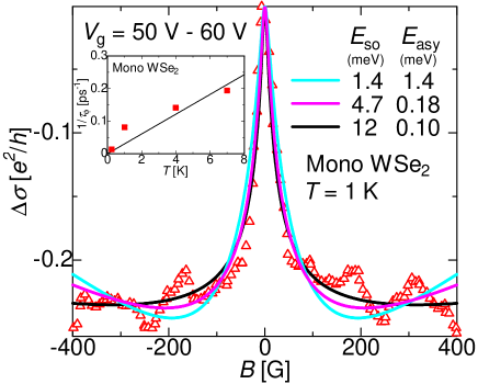
As explained above, equation (1) includes two fitting parameters and . KM and VZ SOI, which are symmetric, determine whereas is attributed to the asymmetric Rashba SOI. Identifying the symmetry of the induced SOI is particularly important to provoke intriguing phenomena such as the QSH effect in graphene. The seminal paper by Kane and Mele kane1 ; kane2 reported that a dominant symmetric SOI is required for the QSH state. From the fitting based on (1), we can determine the ratio between the symmetric and asymmetric contributions to the induced SOI because both () and are fitting parameters. In our previous paper wakamura we demonstrated that for WS2 systems the symmetric SOI is dominant. To evaluate the symmetry of the induced SOI in other systems, in Fig. 9 we show the fits based on different ratios between and in (1). As seen in Fig. 9, when there is no symmetric contribution, the fitting curve (shown in light blue) exhibits a clear upturn in high and largely deviates from the experimental data in the smaller region as well. We note that for it is not possible to fit correctly the data either. To reproduce the flat tail of the experimental data in the high region a dominant symmetric contribution is required, and the best fit is obtained when the spin-orbit scattering strength () is 12 meV. This dominant symmetric contribution is also consistent with the work of zihlmann .
A similar analysis has been performed for all investigated samples. We note that for with a temperature-dependent upturn at high as shown in Fig. 6(b), it is essential to carry out the analysis in small field region. This is because the upturn is attributed to the weak localization contribution, irrelevant to SOI. In the inset of Fig. 6(b), we display the fit of up to = 200 G only by taking into account the weak localization limit ( and ) in (1). The fit reproduces the experimental data well, indicating that weak localization is the main contribution in this limit. On the other hand, it also implies that in this field range there is a large ambiguity to determine and precisely. In Fig. 5(a) and (b) we show the fits of from MoS2 B in small field (Fig. 5(a)) and large field (Fig. 5(b)) region with different ratio between and , where , X = asy or so. While the difference is not as striking as in the case of Mono WSe2 and Mono WS2, in the small field region the large symmetric SOI ( = 70) provides the best fit in comparison with the other two curves ( = 0 and = ) as examples. By contrast, in the high field region, the fits mainly account for a large number of points in the upturn part, where weak localization plays a major role. Indeed, the three fits with different ratio between and provide almost similar curves. Thus to determine the spin-orbit parameters ( and ) accurately, it is indispensable to carry out analysis in a small field region for the samples with temperature-dependent upturn.
In Table 2 we provide the square root of the ratio between and () for all investigated samples. These large ratios of are consistent with other studies wang2 ; valenzuera ; vanwees ; zihlmann .
| Sample | |
|---|---|
| Mono WSe2 | 5.2 - 16 |
| Mono WS2 A | 25 - 53 |
| Mono WS2 B | 22 - 56 |
| Mono MoS2 A | 16 - 64 |
| Mono MoS2 B | 2.7 - 13 |
| Bulk WSe2 | 3.5 - 10 |
| Bulk WS2 A | 2.6 - 21 |
| Bulk WS2 B | 1.9 - 15 |
V.5 Identification of the dominant SOI type from the spin relaxation mechanism
Now that we have found that the symmetric SOI is dominant, we next determine the dominant spin relaxation mechanism since this symmetric SOI is composed of two contributions, KM and VZ SOI. For graphene, there are two possible spin relaxation mechanisms: Elliot-Yafet (EY) and D’yakonov-Perel (DP) mechanism zutic ; fabian ; huetas ; ochoa2 . KM SOI contributes to the EY mechanism mccann since the DP mechanism requires spin-splitting due to inversion symmetry breaking. On the other hand, since VZ SOI roche arises from broken sublattice symmetry, it causes DP-type spin relaxation. We here neglect the contributions from Rashba SOI because the estimates for indicate that Rashba SOI is smaller than the other types of SOI. As reported in previous studies wakamura ; zomer , each contribution (EY or DP) can be determined by fitting the relation between and the momentum relaxation time following the equation
| (3) |
where is the amplitude of spin-orbit coupling leading to EY (DP) mechanism and is the Fermi energy.
In Fig. 10(a) we plot relation (3) for samples with monolayer TMDs in log scale. For all samples including the ones not shown in the figure we found that is larger than , and the ratio varies from 5 to 31 depending on the sample. In the figure of the fitting based on (3), the EY contribution leads to a nonzero -axis intercept, and to the deviations from the straight line in Fig. 10(a). Another way of visualizing the EY contribution is obtained by dividing both sides of (3) by , leading to
| (4) |
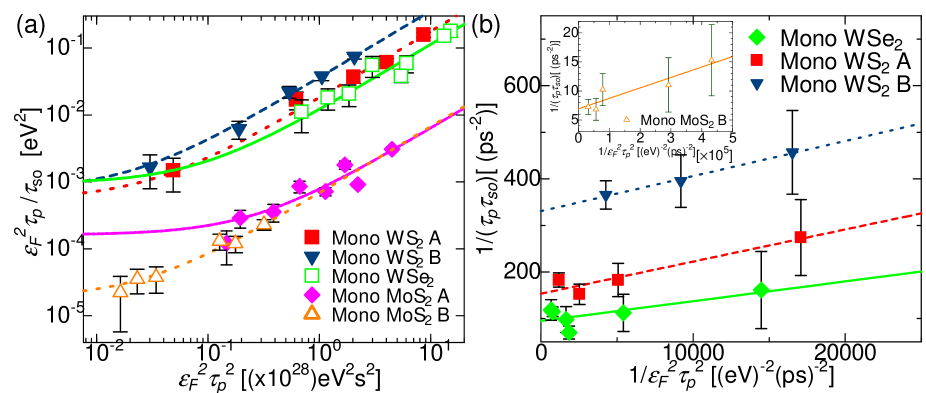
Figure 10(b) shows the relation (4) for three samples with the strongest SOI (Mono WSe2, Mono WS2 A and B). We also plot this relation for Mono MoS2 B in the inset of Fig. 10(b). In these plots the slope of the fit corresponds to the EY contribution. The positive slope that represents the contribution from the EY mechanism is clear for each sample, demonstrating the existence of KM SOI. The fits in Fig. 10(a) and (b) provide somewhat different and , therefore in Table 3 we show the averaged values over the two fits.
The most important difference between the EY and DP spin relaxation mechanism is the different dependence of on the momentum scattering time . While for the EY mechanism, for the DP . In the case of graphene since can be modulated by the ratio between the EY and DP contribution also depends on . This means that depending on the contributions from each SOI (KM or VZ SOI) vary. Hence the EY mechanism, or KM SOI plays an important role particularly around the Dirac point.
We note that if we assume that VZ SOI is the only source of DP spin relaxation, we can replace with in (3), where is the intervalley scattering time roche . Since is always larger than , becomes then even smaller.
| Sample | [meV] | [meV] |
|---|---|---|
| Mono WSe2 | 48.0 12.2 | 3.3 0.10 |
| Mono WS2 A | 27.4 2.8 | 4.4 0.047 |
| Mono WS2 B | 32.9 3.8 | 6.4 0.14 |
| Mono MoS2 A | 10.3 1.7 | 0.87 0.035 |
| Mono MoS2 B | 4.3 0.035 | 0.86 3.5 |
| Bulk WSe2 | 11.6 2.1 | 0.38 0.013 |
| Bulk WS2 A | 8.9 3.7 | 0.73 0.028 |
| Bulk WS2 B | - | 0.72 0.022 |
VI Discussions
VI.1 Possibility of VZ SOI
In the previous section we pointed out the possibility to induce KM SOI in graphene. In contrast, recent ab initio calculations propose the scenario of VZ SOI as the dominant part of the induced SOI. The previous study by Frank et al. frank revealed that VZ SOI generates edge states as KM SOI, but they are not topologically protected. Thus it is of great importance to discuss the possibility of inducing VZ SOI to determine if one can realize the QSH state in graphene on TMD. VZ SOI originates from the sublattice symmetry breaking in graphene. If the sublattice symmetry is broken, different values of the spin-orbit parameter and can appear in the Hamiltonian for symmetric SOI () depending on the sublattice. Thus can be written as gmitra3 :
| (5) |
where , and denote Pauli matrix for sublattice spin, valley spin and real spin, respectively. is the unit matrix in the sublattice space. The terms in equation (5) can then be categorized into two groups according to their dependence on sublattice spin. The first one is proportional to , as the original KM SOI, and expressed as:
| (6) |
where . The second group reads
| (7) |
where . This term is called VZ SOI. To obtain nonzero VZ SOI, is required, thus breaking graphene sublattice symmetry is indispensable.
In the ab initio calculations, the unit cell is composed of (e.g.) 55 graphene and 44 TMD supercells whose bond length have been relaxed in order to generate a perfectly periodic lattice. Experimentally, however, due to a large lattice mismatch between graphene and TMDs (28 %) such a perfect periodicity does not exist gmitra3 . Absence of perfect periodicity is also confirmed by the observations of pseudoperiodic faint Moiré pattern moire1 ; moire2 . Therefore graphene/TMD superlattices are never perfectly periodic moire3 unless the relative rotational angle between two lattices (graphene and TMD) is carefully selected. Slight deviations from the perfect periodicity on a small scale with a few lattices do not provide a considerable effect, but may result in a large deviation in a wider scale and give rise to an equal spin-orbit potential for sublattices A and B on average. Therefore in real graphene/TMD heterostructures the sublattice symmetry may be locally broken on a small scale, but when the average is taken over the mean free path (or intervalley scattering length), which sets a length scale for VZ SOI, the effect of sublattice symmetry breaking might vanish or be considerably suppressed.
On the other hand, the analysis of the spin relaxation mechanisms demonstrated a clear DP contribution although it is much smaller than the EY contribution. Since the other types of SOI (Rashba and pseudospin inversion asymmetry (PIA) SOI) that can provide the DP mechanism are asymmetric, and found to be small by the WAL measurements, we cannot rule out the contribution from VZ SOI to the observed symmetric SOI. Further experimental and theoretical investigations are required for this issue.
It is also interesting to discuss the strength of sublattice symmetry breaking in graphene caused by the underlying TMD layer. A previous report on giant Rashba splitting in graphene due to hybridization with gold gold provides important information. In the calculated band structures, strong Rashba splitting was found with gold adatoms on top of a given sublattice (e.g. sublattice ). It is clear that these gold adatoms break sublattice symmetry, but no sublattice gap is opened between valence and conduction bands unless the distance between graphene and gold atom is unrealistically closer (2.4 Å) than the equilibrium length (3.4 Å). In the case of graphene on TMD, graphene’s orbitals couple to the orbitals of transition metals or orbitals of chalcogen. Taking into account the distance between graphene and TMD (3.4 Å) and also the distance between a transition metal and a chalcogen layer (1.7 Å), it is possible that the sublattice symmetry breaking effect may be small. Angular resolved photoemission spectroscopy (ARPES) studies reported an intact bandstructures of graphene close to the Dirac point in graphene/MoS2 arpes1 ; arpes2 and graphene/WS2 arpes3 heterostructures. It is found that only when the relative angle between graphene and TMD lattice is carefully chosen, minigaps are obtained at high binding energies arpes2 . Based on these previous reports, the effects of the TMD underlayer on the graphene bandstructures may be weak.
VI.2 Suppressed Rashba SOI
From the analysis on the WAL signals we concluded that the induced Rashba SOI is small in comparison with symmetric SOI. Naively, one would have expected instead that strong Rashba SOI is induced in graphene/TMD heterostructures due to the inversion symmetry breaking by the TMD layer. Indeed, some of the previous studies on inducing SOI in graphene by -electron heavy adatoms revealed that strong Rashba SOI is induced gold ; adatom5 ; adatom6 . One of the important differences between graphene/TMD systems and heavy adatoms (e.g. Au) on graphene is that charge transfer between graphene and TMD layers is much weaker than that between adatoms and graphene, as reported by recent ARPES measurements gold ; arpes1 ; arpes2 ; arpes3 . As a result, only a small electric dipole is formed in the graphene/TMD systems compared with adatoms on graphene moire3 . Since a crucial role of charge transfer for Rashba SOI was pointed out theoretically abdel , weak charge transfer effect may be the reason for the small Rashba SOI induced in graphene/TMD heterostructures.
Suppressed Rashba and large SOI proportional to are also consistent with the previous measurements of nonlocal voltages generated by the (inverse) spin Hall effect (SHE) with strong SOI avsar2 . For the SHE, the relation between charge currents , spin polarization of charge currents and generated spin currents is expressed as takahashi . To detect nonlocal voltages in a ”H”-shaped device via the SHE and its inverse, needs to be out-of-plane since and are both inplane. While Rashba SOI provides inplane spin polarization, for KM and VZ SOI the induced spin polarization is out-of-plane. Therefore dominant KM or VZ SOI are required to detect the nonlocal voltages demonstrated in avsar2 .
VI.3 Difference in the amplitudes of the induced SOI in graphene among different TMDs
In the previous sections we demonstrated that there are clear differences in the amplitudes of the SOI induced in graphene by different TMDs. We first discuss the difference among monolayer TMDs.
The analysis of WAL signals showed that MoS2 induces a spin-orbit scattering rate in graphene one order of magnitude smaller than WSe2 and WS2. It is known that MoS2’s intrinsic SOI in the valence band is three times smaller than that of WSe2 and WS2 in the valence band xiao . Considering the relation (3), the inverse spin-orbit time () is proportional to the square of the spin-orbit energy. Therefore the smaller SOI induced in graphene by MoS2 is in agreement with the one order of magnitude difference expected in the spin-orbit amplitudes between graphene/WSe2(or WS2) and graphene/MoS2 heterostructures.
On the other hand, recent ARPES measurements have revealed that the Dirac cone of graphene is closer to the conduction band edge than to the valence band edge of monolayer TMDs arpes1 ; arpes2 ; arpes3 . The spin-splitting of the conduction band edge of monolayer TMDs is neglected in the first approximation due to the nature of the orbital, which has zero orbital magnetic quantum number () xiao . However, recent density functional theory (DFT) calculations point out the importance of the spin-splitting even for the conduction band kosmider ; burkard and provide different spin-splitting estimated for different TMDs. It is very likely that these values have also to be considered to compare the differents SOI induced in graphene.
We also observed a clear difference in the amplitudes of the induced SOI in graphene between monolayer and bulk of the same TMDs. This difference may arise from different surface matching. In general graphene on TMDs is not perfectly flat and there are bubbles and ripples wang2 . Monolayer TMDs are more flexible than bulk TMDs so they could better follow the curvature of the graphene layer. The net area where graphene covered by TMD would thus be greater and the total SOI induced in graphene may be enhanced.
In our previous paper we also proposed that the band structure differences between monolayer and bulk TMD may affect the amplitudes of the induced SOI. However, it is not so likely because no striking differences in the band structure are observed in ARPES measurements between graphene/monolayer MoS2 and graphene/bulk MoS2 samples arpes1 ; arpes2 .
VII Conclusions
In conclusion, we successfully induced strong SOI in graphene by exploiting heterostructures with different TMDs of different thickness. By comparing each system, we observed both universal and nonuniversal characters. Monolayer tungsten-based TMDs (WSe2 and WS2) induce stronger SOI in graphene, while monolayer MoS2 induces SOI one order of magnitude smaller. For WSe2 and WS2, there is a clear difference in the propensity to induce a SOI between monolayer and bulk. Bulk TMDs induce SOI in graphene that is more than one order of magnitude smaller than monolayer ones. Thus we conclude that monolayer WSe2 and WS2 can induce the strongest SOI in graphene.
As a universal behavior, we found that in all systems the induced SOI is predominantly symmetric, composed of KM or VZ SOI. The analysis of the spin relaxation mechanism indicates that the KM SOI plays an important role, especially close to the Dirac point.
While more experimental and theoretical work is still necessary for a deeper understanding, our experimental findings offer new insights on SOI in graphene produced by TMDs, and provide important information for application to spintronics and topological physics.
VIII Acknowledgements
We gratefully acknowledge very useful discussions with V. Fal’ko, A. Meszaros, A. W. Cummings, S. Roche, P. Makk, S. Zihlmann and C. Schönenberger. This project is financially supported in part by the Marie Sklodowska Curie Individual Fellowships (H2020-MSCAIF-2014-659420); the ANR Grants DIRACFORMAG (ANR-14-CE32-003), MAGMA (ANR-16-CE29-0027-02), and JETS (ANR-16-CE30-0029-01), the Overseas Research Fellowships by the Japan Society for the Promotion of Science, the CNRS and the award of a Royal Society University Research Fellowship by the UK Royal Society, the EPSRC grant EP/M022250/1 and the EPSRC-Royal Society Fellowship Engagement Grant EP/L003481/1. M.Q. Zhao and A. T. C. Johnson are supported by the US NSF grant EFRI 2-DARE 1542879.
References
- (1) K. S. Novoselov, A. K. Geim, S. V. Morozov, D. Jiang, Y. Zhang, S. V. Dubonos, I. V. Grigorieva and A. A. Firsov, Science 22, 666 (2004).
- (2) J. T. Ye, Y. J. Zhang, R. Akashi, M. S. Bahramy, R. Arita and Y. Iwasa, Science 338, 1193 (2012).
- (3) X. Xi, Z. Wang, W. Zhao, J.-H. Park, K. T. Law, H. Berger, L. Fórro, J. Shan and K. F. Mak, Nat. Phys. 12, 139 (2016).
- (4) Y. Saito, Y. Nakamura, M. S. Bahramy, Y. Kohama, J. T. Ye, Y. Kasahara, Y. Nakagawa, M. Onga, M. Tokunaga, T. Nojima, Y. Yanase and Y. Iwasa, Nat. Phys. 12, 144 (2016).
- (5) J. M. Lu, O. Zheliuk, I. Leermakers, N. F. Q. Yuan, U. Zeitler, K. T. Law, J. T. Ye, Science 11, 1353 (2015)
- (6) C. Gong, L. Li, H. Ji, A. Stern, Y. Xia, T. Cao, W. Bao, C. Wang, Y. Wang, Z. Q. Qiu, R. J. Cava, S. G. Loui, J. Xia and X. Zhang, Nature 546, 265 (2017).
- (7) B. Huand, G. Clark, E. Navarro-Moratalla, D. R. Klein, R. Cheng, K. Y. Seyler, D. Zhong, E. Schmidgall, M. A. McGuire, D. H. Cobden, W. Yao, D. Xiao, P. Jarillo-Herrero and X. Xu, Nature 546, 270 (2017).
- (8) M. Bonilla, S. Kolekar, Y. Ma, H. C. Diaz, V. Kalappattil, R. Das, T. Eggers, H. R. Gutierrez, M.-H Phan and M. Batzill, Nat. Nanotech. 13, 289 (2018).
- (9) X. Qian, J. Liu, L. Fu and J. Li, Science 346, 1344 (2014).
- (10) Z. Fei, T. Palomaki, S. Wu, W. Zhao, X. Cai, B. Sun, P. Nguyen, J. Finney, X. Xu and D. H. Cobden, Nat. Phys. 13, 677 (2017).
- (11) S. Tang et al., Nat. Phys. 13, 683 (2017).
- (12) S. Wu, V. Fatemi, Q. D. Gibson, K. Watanabe, T. Taniguchi, R. J. Cava and P. Jarillo-Herrero, Science 359, 76 (2018).
- (13) A. A. Soluyanov, D. Gresch, Z. Wang. Q. S. Wu. M. Troyer, X. Dai and A. Bernevig, Nature 527, 495 (2015).
- (14) Z. Wang, D. Gresch, A. A. Soluyanov, W. Xie, S. Kushwaha, X. Dai, M. Troyer, R. J. Cava and B. A. Bernevig, Phys. Rev. Lett. 117, 056805 (2016).
- (15) Y. Sun, S-C. Wu, M. N. Ali, C. Felser and B. Yan, Phys. Rev. B 92, 161107(R) (2015).
- (16) A. K. Geim and I. V. Grigorieva, Nature 499, 419 (2013).
- (17) M. Offidani, M. Milletarì, R. Raimondi and A. Ferreira, Phys. Rev. Lett. 119, 196801 (2017).
- (18) C. L. Kane and E. J. Mele, Phys. Rev. Lett. 95, 226801 (2005).
- (19) C. L. Kane and E. J. Mele, Phys. Rev. Lett. 95, 146802 (2005).
- (20) J. Balakrishnan, G. K. W. Koon, M. Jaiswal, A. H. Castro Neto and B. Özyilmaz, Nat. Phys. 9, 284 (2013).
- (21) M. Gmitra, S. Konschuh, C. Ertler, C. Ambrosch-Draxl and J. Fabian, Phys. Rev. B 80, 235431 (2009).
- (22) A. H. Castro Neto and F. Guinea, Phys. Rev. Lett. 103, 026804 (2009).
- (23) C. Weeks, J. Hu, J. Alicea, M. Franz and R. Wu, Phys. Rev. X 1, 021001 (2011).
- (24) J. Hu, J. Alicea, R. Q. Wu and M. Franz, Phys. Rev. Lett. 109, 266801 (2012).
- (25) J. Balakrishnan et al., Nat. Commun. 5, 4748 (2014).
- (26) F. Calleja, et al., Nat. Phys. 11, 43 (2015).
- (27) L. Brey, Phys. Rev. B 92, 235444 (2015).
- (28) I. I. Klimovskikh et al., ACS Nano 11(1), 368 (2017).
- (29) D. Marchenko, A. Varykhalov, M. R. Scholz, G. Bihlmayer, E. I. Rashba, A. Rybkin, A. M. Shikin and O. Rader, Nat. Commun. 3, 1232 (2012).
- (30) D. Xiao, G. B. Liu, W. Feng, X. Xu and W. Yao, Phys. Rev. Lett. 108, 196802 (2012).
- (31) A. Avsar et al., Nat. Commun. 5, 4875 (2014).
- (32) Z. Wang, D. K. Ki, H. Chen, H. Berger, A. H. MacDonald and A. F. Morpurgo, Nat. Commun. 6, 8339 (2015).
- (33) Z. Wang, D. K. Ki, J. Y. Khoo, D. Mauro, H. Berger, L. S. Levitov, and A. F. Morpurgo, Phys. Rev. X 6, 041020 (2016).
- (34) B. Yang et al., 2D Mater. 3, 031012 (2016).
- (35) B. Yang, M. Lohmann, D. Barroso, I. Liao, Z. Lin, Y. Liu, L. Bartels, K. Watanabe, T. Taniguchi and J. Shi, Phys. Rev. B 96, 041409 (R) (2017).
- (36) M. Gmitra and J. Fabian, Phys. Rev. B 92, 155403 (2015).
- (37) M. Gmitra, D. Kochan, P. Högl, and J. Fabian, Phys. Rev. B 93, 155104 (2016).
- (38) A. W. Cummings, J. H. Garcia, J. Fabian, and S. Roche, Phys. Rev. Lett. 119, 206601 (2017).
- (39) T. P. Cysne, A. Ferreira and T. G. Rappoport, Phys. Rev. B 98, 045407 (2018).
- (40) M. Offidani and A. Ferreira, Phys. Rev. B 98, 245408 (2018).
- (41) S. Ilić, J. S. Meyer and M. Houzet, arxiv:1808.05872.
- (42) A. M. Alsharari, M. M. Asmar and S. E. Ulloa, Phys. Rev. B 98, 195129 (2018).
- (43) L. A. Benitez, J. F. Sierra, W. S. Torres, A. Arrighi, F. Bonnell, M. V. Costache and S. O. Valenzuera, Nat. Phys. 14, 303 (2018).
- (44) T. S. Ghiasi, J. Ingla-Aynés, A. A. Kaverzin and B. J. van Wees. Nano Lett. 17, 7528 (2017).
- (45) T. Frank, P. Högl, M. Gmitra, D. Kochan and J. Fabian, Phys. Rev. Lett. 120, 156402 (2018).
- (46) S. Zihlmann, A. W. Cummings, J. H. Garcia, M. Kedves, K. Watanabe, T. Taniguchi, C. Schonenberger, and P. Makk, Phys. Rev. B 97, 075434 (R) (2018).
- (47) T. Wakamura, F. Reale, P. Palczynski, S. Gueron, C. Mattevi, and H. Bouchiat, Phys. Rev. Lett. 120, 106802 (2018).
- (48) T. Volkl, T. Rockinger, M. Drienovsky, K. Watanabe, T. Taniguchi, D. Weiss and J. Eroms, Phys. Rev. B, 96, 125405 (2017).
- (49) S. Ringer, S. Hartl, M. Rosenauer, T. Volkl, M. Kadur, F. Hopperdietzel, D. Weiss and J. Eroms, Phys. Rev. B, 97, 205439 (2018).
- (50) H. C. Diaz, J. Avila, C. Chen, R. Addou, M. C. Asensio and M. Batzill, Nano Lett. 15, 1135 (2015).
- (51) D. Pierucci et al., Nano Lett. 16, 4054 (2016).
- (52) H. Henck, Z. Ben Aziza, D. Pierucci, F. Laourine, F. Reale, P. Palczynski, J. Chaste, M. G. Silly, F. Bertran, P. LeFevre, E. Lhuillier, T. Wakamura, C. Mattevi, J. E. Rault, M. Calandra, and A. Ouerghi, Phys. Rev. B 97, 155421 (2018).
- (53) C.-I Lu et al., 2D mater. and Appl. 1, 24 (2017).
- (54) C.-I Lu et al., Appl. Phys. Lett. 106, 181904 (2015).
- (55) H. C. Diaz, R. Addou and M. Batzill, Nanoscale 6, 1071 (2014).
- (56) G. Bergmann, Phys. Rep. 107, 1 (1984).
- (57) T. Ando, T. Nakanishi and R. Saito, J. Phys. Soc. Jpn. 67, 2857 (1998).
- (58) H. Suzuura and T. Ando, Phys. Rev. Lett. 89, 266603 (2002).
- (59) S. V. Morozov, K. S. Novoselov, M. I. Katsnelson, F. Schedin, L. A. Ponomarenko, D. Jiang and A. K. Geim, Phys. Rev. Lett. 97, 016801 (2006).
- (60) X. Wu, X. Li, Z. Song, C. Berger and W. A. de Heer, Phys. Rev. Lett. 98, 136801 (2007).
- (61) F. V. Tikhonenko, D. W. Horsell, R. V. Gorbachev and A. K. Savchenko, Phys. Rev. Lett. 100, 056802 (2008).
- (62) F. V. Tikhonenko, A. A. Kozikov, A. K. Savchenko and R. V. Gorbachev, Phys. Rev. Lett. 103, 226801 (2009).
- (63) E. McCann and V. I. Fal’ko, Phys. Rev. Lett. 108, 166606 (2012).
- (64) F. Reale et al., Sci. Rep. 7, 14911 (2017).
- (65) K. Kośmider, J. W. González and J. Fernández-Rossier, Phys. Rev. B 88, 245436 (2013).
- (66) A. Kormányos, V. Zólyomi, N. D. Drummond and G. Burkard, Phys. Rev. X 4, 011034 (2014).
- (67) J. H. Garcia, M. Vila, A. W. Cummings and S. Roche, Chem. Soc. Rev. 47, 3359 (2018).
- (68) A. Klein, S. Tiefenbacher, V. Eyert, C. Pettenkofer and W. Jaegermann, Phys. Rev. B 64, 205416 (2001).
- (69) A. Ramasubramaniam, D. Naveh, and E. Towe, Phys. Rev. B 84, 205325 (2011).
- (70) H. Terrones, F. Loópez-Urias and M. Terrones, Sci. Rep. 3, 1549 (2013).
- (71) B. Grbić, R. Leturcq, T. Ihn, K. Ensslin, D. Reuter and A. D. Wieck, Phys. Rev. B 77, 125312 (2008).
- (72) E. McCann, K. Kechedzhi, V. I. Fal’ko, H. Suzuura, T. Ando and B. L. Altshuler, Phys. Rev. Lett. 97, 146805 (2006).
- (73) I. Žutić, J. Fabian and S. Das Sarma, Rev. Mod. Phys. 76, 323 (2004).
- (74) J. Fabian and S. Das Sarma, J. Vac. Sci. Technol. B 17, 1708 (1999).
- (75) D. Huertas-Hernando, F. Guinea and A. Brataas, Phys. Rev. Lett. 103, 146801 (2009).
- (76) H. Ochoa, A. H. Castro Neto and F. Guinea, Phys. Rev. Lett. 108, 206808 (2012).
- (77) P. J. Zomer, M. H. D. Guimarães, N. Tombros and B. J. van Wees, Phys. Rev. B 86, 161416(R) (2012).
- (78) A. Varykhalov, J. Sánchez-Barriga, A. M. Shikin, C. Biswas, E. Vescovo, A. Rybkin, D. Marchenko and O. Rader, Phys. Rev. Lett. 101, 157601 (2008).
- (79) D. Marchenko, J. Sánchez-Barriga, M. R. Scholz, O. Rader and A. Varykhalov, Phys. Rev. B 87, 115426 (2013).
- (80) S. Abdelouahed, A. Ernst, J. Henk, I. V. Maznichenko and I. Mertig, Phys. Rev. B 82, 125424 (2010).
- (81) S. Takahashi and S. Maekawa, Sci. Technol. Adv. Mater. 9, 014105 (2008).
- (82) N. J. G. Couto, D. Costanzo, S. Engels, D-. K. Ki, K. Watanabe, T. Taniguchi, C. Stampfer, F. Guinea and A. F. Morpurgo, Phys. Rev. X 4, 041019 (2014).