Probing Quantum Confinement and Electronic Structure at Polar Oxide Interfaces
Polar discontinuities occurring at interfaces between two different materials constitute both a challenge and an opportunity in the study and application of a variety of devices. In order to cure the large electric field occurring in such structures, a reconfiguration of the charge landscape sets in at the interface via chemical modifications, adsorbates or charge transfer. In the latter case, one may expect a local electronic doping of one material: one sparkling example is the two-dimensional electron liquid (2DEL) appearing in SrTiO3 once covered by a polar LaAlO3 layer. Here we show that tuning the formal polarisation of a (La,Al)1-x(Sr,Ti)xO3 (LASTO:) overlayer through chemical composition modifies the quantum confinement of the 2DEL in SrTiO3 and its electronic band structure. The analysis of the behaviour in magnetic field of superconducting field-effect devices reveals, in agreement with ab initio calculations and self-consistent Poisson-Schrödinger modelling, that quantum confinement and energy splitting between electronic bands of different symmetries strongly depend on interface charge densities. These results not only strongly support the polar discontinuity mechanisms with a full charge transfer to explain the origin of the 2DEL at the celebrated LaAlO3/SrTiO3 interface, but also demonstrate an effective tool for tailoring the electronic structure at oxide interfaces.
Functionalities offered by the interfaces between different materials have been the fundamental basis of modern electronic devices and information technology SchenkelNatMat2005 ; SzeBook2006 . Transition metal oxides (TMOs), largely owing to their correlated electrons and entanglement of various degrees of freedom, provide an ideal platform for establishing a variety of novel electronic properties TokuraScience2000 ; CheongNatMat2007 . In recent years, a burst of research activities on heterostructures of transition metal oxides has been driven by the quest for emergent phenomena at interfaces that are absent in the bulk parent compounds HwangNatMatRev2012 . Indeed, at the interface, different phenomena are at play, including symmetry breaking, electrostatic coupling, atomic rearrangement, etc. ZubkoAnnRev2011 ; ChakhalianRevModPhys2014 . One phenomenon particularly relevant for transition metal ions with multiple valence states is charge transfer. This effect has been suggested to be the origin of several recently discovered novel electronic states: its driving force has been attributed to differences in cationic electron affinity for instance in LaNiO3/LaMnO3 GibertNatMat2012 ; LeePRB2013 or CaMnO3/CaRuO3 TakahashiAPL2001 ; HePRL2012 , or to charge delocalisation in LaTiO3/SrTiO3 OhtomoNature2002 ; OkamotoNature2004 or LaMnO3/SrMnO3 MayNatMat2009 ; SmadiciPRL2007 heterostructures.
For the LaAlO3 (LAO)/SrTiO3 (STO) interface, the polar discontinuity has often been regarded as the origin of the charge transfer OhtomoNature2004 ; NakagawaNatMat2006 ; ThielScience2006 ; LeiNPJ-QM2017 and the formation of a superconducting two dimensional electron liquid (2DEL) ReyrenScience2007 ; CavigliaNature2008 . The formal polarisation of LAO due to the (LaO)+ and (AlO2)- atomic planes is disrupted along the [001] direction by the non-polar STO, since (SrO)0 and (TiO2)0 planes are formally charge neutral. Density-functional theory (DFT) calculations PopovicPRL2008 ; PentchevaJPCM2010 for a defect-free interface show that the build-up of the electric potential inside LAO leads to a Zener breakdown NakagawaNatMat2006 and a progressive charge transfer of 0.5 electrons per surface unit cell (0.5 e-/u.c.) from the LAO surface O- states to the interfacial Ti- states, thus forming a 2DEL. This mechanism successfully explains the observed threshold LAO thickness, , of 4 unit cells (u.c.) for the onset of conductivity ThielScience2006 , but faces questions raised by several experiments, reporting, for instance, the lack of O- hole-pockets BernerPRL2013 or a weak initial electric field in LAO BernerPRB2013 ; SegalPRB2009 ; SlootenPRB2013 . Relying on polar discontinuity and the formation of oxygen vacancies at the LAO surface, recent theoretical work BristowePRB2011 ; BristoweJPCM2014review ; YuZungerNatComm2014 ; ZhouPRB2015 predicts a similar critical thickness , while solving some of the discrepancies mentioned above.
Reinle-Schmitt et al. ReinleNatComm2012 showed that polar discontinuity and critical thickness are indeed correlated: tuning the polar discontinuity by alloying LAO with STO [(La,Al)1-x(Sr,Ti)xO3, denoted as LASTO:], increases, with an inverse proportionality to the fraction of LAO in the alloy and therefore with the formal polarisation, in perfect agreement with DFT predictions. The self-confinement of the transferred charge leads to an electronic reconstruction of the Ti bands, increasing the energy of -symmetry states by 50 meV with respect to the states SalluzzoPRL2009 ; DelugasPRL2011 . This band structure differs from the electronic structure of bulk STO vanderMarelPRB2011 , and is at the origin of the unique electronic properties of the LAO/STO interface. However, the carrier density () measured using Hall effect at the LASTO:0.5/STO interface was found to be comparable to the one of the standard LAO/STO interface (of the order of 1013 cm-2) ReinleNatComm2012 , a value significantly lower than the theoretical prediction based on the polar discontinuity scenario (= 1.71014 cm-2 or 0.25 e-/u.c. for the LASTO:0.5/STO interface and 3.31014 cm-2 or 0.5 e-/u.c. for the LAO/STO interface). This discrepancy between the predicted and measured carrier densities has been one important open issue questioning the origin of the 2DEL and has been related to different mechanisms, such as charge localization PopovicPRL2008 ; TakizawaPRB2011 ; CancellieriStrocovBook2018 due to interface disorder, surface defects and selective quantum confinement in a single layer, or to anti-site defects YuZungerNatComm2014 , or to phase separation AriandoNatComm2011PhaseSeparation .
Here we probe the quantum confinement and its consequences on the electronic band structure at the superconducting LASTO:0.5/STO interface and compare the results with standard LAO/STO interfaces. Using sophisticated superconductivity measurements and DFT-complemented Poisson-Schrödinger modelling, we provide strong evidences that, although transport measures a fraction of the carriers predicted by the polar discontinuity scenario, the full amount of charge is indeed present at the interfaces. The field-effect tuning of the superconducting state suggests that the energy splitting between bands of different symmetries ( vs. ) is reduced with the widening of the confining potential, in agreement with the models. Our results strongly support that charges with nominal carrier densities of 0.5 e-/u.c. and 0.25 e-/u.c. for the LAO/STO and LASTO:0.5/STO interfaces respectively contribute to the electronic confinement and only these total carrier densities can explain the differences in the extension of the 2DEL and in their electronic configurations.
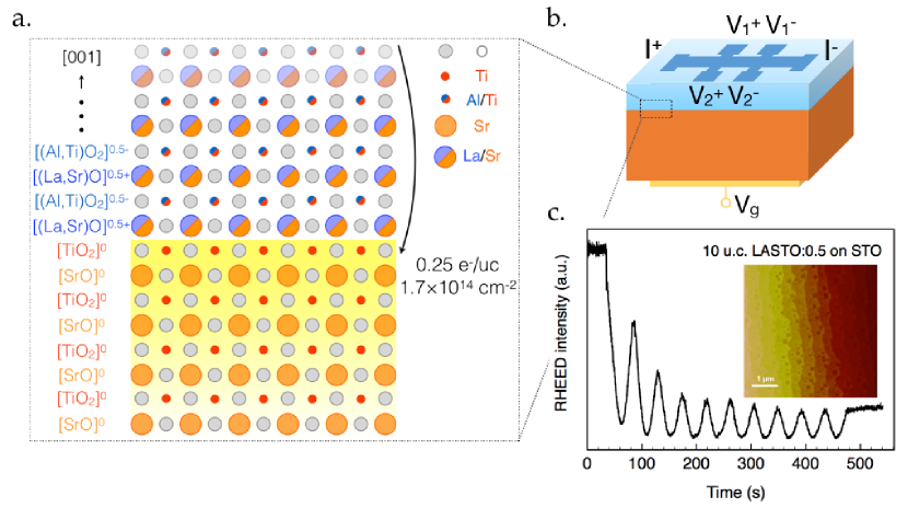
Figure 1a shows a schematic of the atomic structure of the LASTO:0.5/STO interface with the La/Sr and Al/Ti cations spread evenly on the AO and BO2 perovskite planes according to energy calculations performed by DFT ReinleNatComm2012 . Consequently, along the direction, the layer has alternating planes with formal electronic charges of and per unit cell (u.c.). The polar discontinuity is therefore half the one of standard LAO/STO interfaces. As a result, the density of the transferred charges to the interface is estimated to be 0.25 e-/u.c. ( 1.71014 cm-2). LASTO:0.5 films were grown by pulsed-laser deposition (PLD) using growth conditions described in Experimental Section. The oscillations of the reflection high-energy electron diffraction (RHEED) intensity provide a measure of the thickness of the layer during the growth, as shown in Figure 1c for a 10 u.c. film. Topographic scan using atomic force microscopy (AFM) shows a sharp step-and-terrace structure on the film surface with single-unit-cell step height (Figure 1c inset). Both RHEED and AFM data indicate a high growth quality of the films. We note that, in order to probe the intermixing strength and the sharpness of the LASTO:0.5/STO interface, detailed scanning transmission electron microscopy (STEM) study is required. Hall bars (see Figure 1b) were defined using a pre-patterning technique for transport measurements CancellieriEPL2010 . A gate electrode was deposited at the backside of the STO substrate (see Figure 1b) in order to tune the properties of the electron liquid. Transport measurements were performed in a dilution cryostat equipped with a rotating sample holder allowing the orientation of the magnetic field to be varied from perpendicular to parallel to the interface plane.
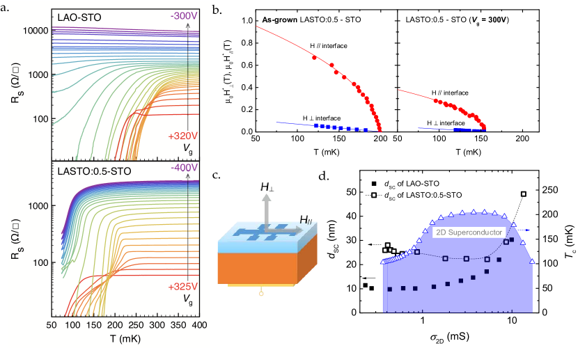
A superconducting ground state is observed when the sample is cooled below a critical temperature, , of 200 mK, generally lower than that of the LAO/STO system (see discussions) CavigliaNature2008 . In Figure 2b we show the critical magnetic field for perpendicular and parallel orientation of a LASTO:0.5/STO interface in its virgin state. The critical temperature for each magnetic field was defined as the temperature at which the sheet resistance reaches half the normal state value (estimated at 500 mK). We calculate the in-plane coherence length from the Ginzburg-Landau formula using the perpendicular field (Equation 1) and we extrapolate for a value of 55 nm, similar to the one observed for standard interfaces ReyrenAPL2009 .
| (1) |
The temperature dependence of the parallel critical field follows the 2D behaviour of a superconducting thin film TinkhamBook1996 . We then use Equation 2 for a 2D superconductor to calculate its thickness from the value of :
| (2) |
We obtain a value 24 nm, independent of the temperature as expected, a value that is larger by a factor of 2 than the one of LAO/STO interfaces CopiePRL2009 ; DubrokaPRL2010 ; ReyrenAPL2009 . We note that the thickness obtained from the analysis of the anisotropic superconducting properties is a characteristic thickness which, in the case of pure LAO/STO, was found to agree well with the vertical spread of the electron system determined using other methods CopiePRL2009 ; DubrokaPRL2010 .
Field effect was then used to tune the doping level and the superconducting properties of the interface. Figure 2a shows the modulation of the superconducting transitions when the gate voltage is varied from V to V, in comparison with the data of the LAO/STO interface CavigliaNature2008 . We observe that and the normal state resistance (see Supporting Information for the vs. plot) are effectively tuned; we note however that for the largest negative voltages, i.e. in the strongest depletion regime, the system remains metallic and superconducting and we do not attain the insulating state reported for standard LAO/STO interfaces (top panel in Figure 2a). The presence of superconductivity and relatively high conductance at largest negative voltages can be related to the occupation of -symmetry states, even at lowest doping levels, at the LAOSTO:0.5/STO interface and will be discussed below. The evolution of versus (sheet conductance in the normal state), illustrated in Figure 2d, shows a dome-like behaviour, reaching a maximum of 206 mK. For several gate voltages, the parallel and perpendicular critical magnetic fields were measured: data for V is shown in the right panel of Figure 2b. These measurements allow us to estimate the superconducting layer thickness across the phase diagram. This information is shown in Figure 2d, where the superconducting thickness for LASTO:0.5/STO samples is displayed in comparison with LAO/STO interfaces. We see that the thickness for the alloy samples is larger than that of standard interfaces across the phase diagram: of LASTO:0.5/STO interfaces falls in the range of 20-30 nm for a wide interval of conductances, while it remains 10-15 nm for the LAO/STO interface. Assuming that this superconducting thickness mirrors an effective width of the confining potential, we attribute this enhancement to the difference in the transferred charge due to a modified polar discontinuity.
To support this idea, we model the quantum confinement at these oxide interfaces using two complementary approaches, first-principles calculations and Poisson-Schrödinger (P-S) approach JanottiPRB2012 .
Previous DFT studies on LAO/STO interfaces DelugasPRL2011 ; LeePRB2008 ; YamamotoAPL2014 ; JanottiPRB2012 ; ReshakJAP2016 ; CancellieriPRB2014 ; GuJPCC2012 have investigated the fully compensated interface (3.3 1014 cm-2) through symmetric superlattices (with two -type interfaces). Lower carrier densities have been reached by artificially removing some charges at the interface and compensating by a positive background DelugasPRL2011 ; CancellieriPRB2014 . In our study, the interfacial charge is directly modified by explicitly tuning the polar discontinuity, i.e. by switching LAO to LASTO:0.5 solid solution. In the following, we present the two doping cases, 0.5 e-/u.c. and 0.25 e-/u.c. for (LAO)2/(STO)30 and (LASTO:0.5)2/(STO)30 superlattices (each with 330 atoms, see Supporting Information) . For the purpose of describing the charge profile at the interface, we set the extension of the STO block as wide as possible for numerical calculations (much larger than previous studies DelugasPRL2011 ; CancellieriPRB2014 ). The calculations also provide physical parameters used later in the P-S modelling.
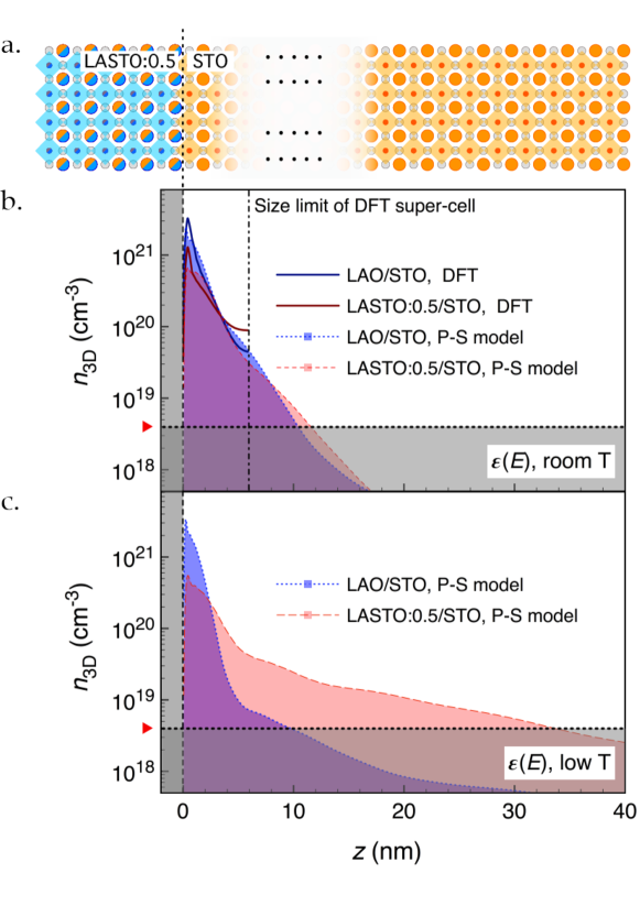
Figure 3 illustrates a sketch of the LASTO:0.5/STO system (Figure 3a) and compares the main results from the calculations. The dashed line indicates the position of the interface. The DFT computed charge profile for the two interfaces is displayed in Figure 3b. The vertical dot-dashed line denotes the extension of the largest STO supercell. Performing calculations for different sizes of the STO supercell, we have noticed that the charge profile extends further into the substrate each time we increase the supercell width, but this occurs on a logarithmic charge density scale (see Supporting Information). Looking at the plot, we see that most of the carriers are located in the first unit cells in both cases; moving away from the interface, a crossing between the two profiles occurs (at 3.5 nm): for lower carrier density, the charge is more spread into the supercell while for higher density it is more localized close to the interface. These calculations rely on the self-consistent DFT dielectric constant ( = 250 in zero field) that reflects the behaviour of STO at room temperature.
To access the low temperature case which is experimentally measured, we need to overcome some limitations of the DFT approach: (i) the STO size limit in the numerical calculations and (ii) the low temperature diverging value of the dielectric constant that is not captured. To bypass these limitations, a self-consistent P-S model using DFT data is employed SternPRB1972 . Effective mass values are obtained from DFT calculations. We notice that the effect of the renormalization of due to, for instance, polaronic effects DubrokaPRL2010 ; CancellieriNatComm2016 , has also been examined (See Supporting Information): while this renormalization indeed slightly affects the calculated charge distribution, it does however not alter the main findings, discussions and conclusions below. The field dependence of the dielectric constant is adjusted according to the measurements PeelaersAPL2015 (details can be found in Experimental Section and Supporting Information).
The resulting profile for the room-temperature configuration ( = 250) is first compared with the DFT data in Figure 3b: the two approaches provide similar charge density profiles (especially in the regime close to the interface), therefore validating the P-S model with respect to the DFT calculations; it further highlights that, although large and at the computation limit, the size of the DFT supercells is still too small to correctly describe the tail of the carrier density profile, which is better accessible in the P-S simulation. From the latter we determine that for both surface carrier densities, the spatial extension at the 3D density threshold for the occurrence of superconductivity ( 41018 cm-3, labelled in Figure 3b) KooncePR1967STO is 10 nm. We note that the thickness of the 2DEL estimated by different techniques differs a lot – from a few u.c. to 10 nm BasleticNatMat2008 ; CopiePRL2009 ; SingPRL2009 ; CancellieriPRL2013 . This may be due to the high density in the first few atomic layers of STO that is decaying by a factor of 10 in 5 nm. The tail of this distribution may fall below the sensitivity of some of the techniques used to probe the 2DEL thickness.
At low temperature, increases due to the quantum paraelectric behaviour of STO: in this regime, the field dependence is described by Equation 3 (see Experimental Section and Figure S3 for details). Using this dependence, the charge density profiles () are calculated using the P-S model for the two interfaces and are illustrated in Figure 3c. We see that the effect of the large is to open the confining potential for the LASTO:0.5/STO interface with more charges spreading into STO. At the (labelled in Figure 3c), the extension of the 2DEL is 10 nm for the LAO/STO interface and 31 nm for the LASTO:0.5/STO interface, values that agree with the estimation of the superconducting thickness extracted from the critical field measurements discussed above. This suggests that the change in superconducting thickness and the confinement scale at the LASTO:0.5/STO interface is due to a reduced total charge density originating from a modified polar discontinuity (see discussion below). The modelling also clearly shows that the dielectric properties of STO and the total 2D carrier density define the confinement of the charge, in agreement with a recent tight-binding study RaslanPRB2017 . We note that, at low temperature, the P-S modelling gives a lower integrated charge density for () above (blue area above the dotted line in Figure 3c as compared to that in Figure 3b). This is also due to the remarkable temperature dependence of and the large electric field dependence of at low temperature: a portion of the charges extends further into STO, with density below .
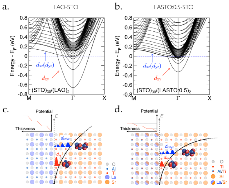
The effect of the surface carrier density and the quantum confinement on the electronic band structures calculated from DFT for the two superlattices (STO)30/(LAO)2 and (STO)30/(LASTO:0.5)2 is displayed in Figure 4, panels a and b. The Fermi level lies at and the symmetry of the electronic states ( and ) is indicated by an arrow. We see changes in the splittings between sub-bands as well as between bands with different symmetry: for a larger extension of the 2DEL (LASTO:0.5/STO, panel b), the sub-band spacing is reduced and the / bands are occupied at lower densities. The calculated bottom of the first / band relative to Fermi level depends on the size of the superlattices, which is discussed in Supporting Information (Figure S8).
The agreement between the experimental estimation of the superconducting layer thickness and the theoretical calculations provides strong support to the polar discontinuity as the doping mechanism of the interfaces. Despite the similar mobile carrier densities extracted from Hall measurements for the two interfaces ReinleNatComm2012 , calculations and superconducting critical fields measurements show that the increase in the characteristic thickness of the 2DEL for the LASTO:0.5/STO interface is a direct result of the reduced total transferred charges (from 0.5 to 0.25 e-/u.c.) upon modification of the polar discontinuity. Although a large fraction of these charges does not contribute to electric transport, it defines the strength of the electric field in STO and consequently its dielectric constant at the interface, that finally sets the extension of the 2DEL. In fact, considering only a charge density extracted from Hall measurements ( 0.05 e-/u.c.) at the interfaces in P-S calculations would result in an ineffective electric field and de-confinement of the electrons with the spatial extension over 60 nm at density of . This demonstrates that all charges with nominal charge density predicted by the polar discontinuity mechanism are transferred to the interface. Our results show significant differences from the work by Ueno et al. UenoPRB2014 , where, experimentally, no dependence of the superconducting thickness on the electrostatically-tuned carrier density was observed.
The consequence of the larger charge profile at the LASTO:0.5/STO interface is a band structure with larger contribution of the bands to the density of states, as shown in Figure 4b. We argue that this electronic configuration is the reason for the modified phase diagram of the superconducting state of the LASTO:0.5/STO interface presented in Figure 2. The overall lower observed in the system, as compared with that of the LAO/STO interface, can be due to a shallow confining potential, which gives a reduced effective as the extension increases GariglioAPLMater2016 ; ValentinisPRB2017 . Furthermore, we observe that field effect is not efficient enough to deplete the 2DEL in order to suppress superconductivity nor to reach a highly resistive state. This is clearly different from the LAO/STO system. The presence of superconductivity and the low resistance state in the depletion regime suggest that the -symmetry states are occupied even at low dopings due to reduced energy splittings between bands, highlighting the relevance of these orbitals on superconductivity and high electron mobility at the interfaces.
Our study provides a direct comparison between ab initio calculations performed on a massive supercell and the self-consistent P-S modelling, revealing that the latter method is also valid to describe quantum confinement of oxide systems where electronic states are more spatially localised than bands in semiconductor. The ab initio calculations of the effective masses combined with the experimental determination of the dielectric properties allow the P-S modelling to describe the field and charge configuration on scales that today cannot be achieved by DFT methods.
To conclude, we have demonstrated that by doping LAO films with STO to form a 50 % alloy compound we are able to successfully change the polar discontinuity at this (super-)conducting interface. This modulation leads to a significant change in the interfacial confining potential that we have estimated from the measurements of the characteristic superconducting thickness. The evolution of the confinement with the change in polarization is captured by advanced large-scale DFT calculations and self-consistent Poisson-Schrödinger modelling, only when assuming that a full transfer of charges takes place at the LAO/STO interface with the density predicted by the polar catastrophe model using first-principle calculations. The resulting band structure for the LASTO:0.5/STO interface reveals a larger contribution of the bands to the density of states and explains the persistence of the superconducting state in the depletion regime. This study shows that the control of the polar discontinuity at oxide interfaces by chemical composition is an effective tool for engineering novel electronic states in these compounds.
I EXPERIMENTAL SECTION
I.1 Sample preparation
Prior to film deposition, Hall-bar patterns with the crystalline TiO2-terminated surface of (001) single-crystal STO substrates were defined using photolithography, followed by a subsequent amorphous STO deposition used as hard mask and lift-off process. Films were then grown by pulsed-laser deposition using standard growth conditions FeteAPL2015 : a KrF laser ( nm) with a pulse energy of mJ ( J cm-2), repetition rate of Hz; growth temperature of C, O2 pressure of mbar; samples were cooled after growth to C in mbar O2 and maintained at this temperature and pressure for one hour before being cooled down to room temperature in the same atmosphere. The growth rate was approximately laser pulses per monolayer. The deposition was fully monitored by RHEED and specular spot intensity oscillations indicate a layer-by-layer growth. RBS analysis reveals a film stoichiometry in agreement, within the experimental uncertainties (1.5 %), with the nominal concentration of for a -nm-thick film.
I.2 Field-effect device and superconductivity measurements
Aluminium wires were ultra-sonically bonded to the sample. Gold pad was deposited by sputtering on the back side of the sample as back-gate electrode. A dc bias was applied across the STO substrate between back gate and the conducting interface. Superconductivity measurements were performed in a 3He/4He dilution refrigerator (Leiden Cryogenics) with a base temperature of 50 mK and a superconducting magnet allowing field of up to 15 T to be reached. Samples were attached to a rotator head for anisotropic magnetic field measurements. Precise parallel and perpendicular orientations with respect to the magnetic field were determined using both longitudinal resistance and Hall resistance . In the parallel direction, an off-axis angle is estimated to be smaller than 0.02∘ from the signal. Current was applied to the conducting channel from a Keithley 6220 high precision current source. Voltages were recorded using Keithley 2182 nanovolt meters.
I.3 DFT calculations
First-principles calculations have been performed with the CRYSTAL code (refcrystal14, ), which implements the Kohn-Sham ansatz to density functional theory kohnsham using a Linear Combination of Atomic Orbital (LCAO) approach and local gaussian basis sets. Electronic exchange-correlation effects were described with the B1-WC hybrid functional dbilcb1wc , including of Hartree-Fock exact exchange. Sampling of the Brillouin zone with a Monkhorst-Pack monkhorstpack1972 k-point mesh ensures a proper convergence of the total energy at the self-consistent field level, with a threshold criterium of . The electronic properties are computed using a refined k-point mesh. A gaussian smearing of the Fermi surface has been set to . The basis sets used for different atoms are detailled in Ref. tibasisset for Ti, Ref. osrbasisset for O, Ref. albasisset for Al and Ref. labasisset for La, and correspond to the ones used in Ref. ReinleNatComm2012 . The optimisation of the atomic positions is performed with convergence criteria of in the root-mean square values of the energy gradients, and in the root-mean square values of the atomic displacements. The evaluation of the Coulomb and exchange series is determined by five parameters, fixed to their default refcrystal14manual values: 7, 7, 7, 7 and 14. Calculations are performed on off-stoichiometric and : superlattices, with two n-type interfaces, with an additional plane in STO, and an additional () plane in LAO (). The effective masses associated to the different Ti band are calculated. Each band has two light effective masses associated to the light carriers and one heavy effective mass associated to the heavy carriers (for Ti , and ). With both superlattices, we have = 0.4 and = 5.9 (very close to the calculated values in cubic STO: = 0.4 and = 6.1 ).
I.4 P-S modelling
Starting from the band structure at the LAO/STO interface suggested by DFT calculations DelugasPRL2011 , we model the confinement, energy levels, and charge distribution at both interfaces by self-consistently solving the Poisson and Schrödinger equations SternPRB1972 . For the boundary conditions of the potential profile , we consider that the LAO or the LASTO:0.5 layer fixes the displacement field at the interface to be = with = 0.5 or 0.25 e-/u.c., respectively, while = 0 at the bottom side of STO. The static dielectric constant of STO calculated by DFT ( = 250) was used as the room-temperature static . The low-temperature static was obtained from a fit to our experimental data ( = 25462). For both temperatures, the high-field dependent is estimated from Stengel StengelPRL2011 . takes the general form:
| (3) |
with = 250, = 107 V m-1 for room temperature, and = 25462, = 82213 V m-1 for low temperature, respectively (see Supporting Information).
For details of the calculation, the algorithm used for convergence of the self-consistency calculations, please refer to FeteThesis2014 . The field dependence of can be found in Supporting Information.
II Acknowledgments
Danfeng Li and Sébastien Lemal contributed equally to this work. We thank C. Cancellieri for providing the target and M. Gabay for useful discussions. This work was supported by the Swiss National Science Foundation – division II, and has received funding from the European Research Council under the European Union Seventh Framework Programme (FP7/2007-2013)/ERC Grant Agreement No. 319286 (Q-MAC). The present research also benefits from computational resources made available on the Tier-1 supercomputer of the Fédération Wallonie-Bruxelles, infrastructure funded by the Walloon Region under the grant agreement 1117545. Computational resources have been provided by the Consortium des Équipements de Calcul Intensif (CÉCI), funded by the Fonds de la Recherche Scientifique de Belgique (F.R.S.-FNRS) under Grant No. 2.5020.11. Ph. G. and S. L. acknowledge financial support from F.R.S.-FNRS PDR project HiT-4FiT and from ARC project AIMED.
References
- (1) Schenkel, T. Semiconductor physics: reliable performance. Nature Materials 4, 799–800 (2005).
- (2) Sze, S. M. & Ng, K. K. Physics of semiconductor devices (John Wiley & Sons, 2006).
- (3) Tokura, Y. & Nagaosa, N. Orbital physics in transition-metal oxides. Science 288, 462–468 (2000).
- (4) Cheong, S.-W. Transition metal oxides: the exciting world of orbitals. Nature Materials 6, 927–928 (2007).
- (5) Hwang, H. et al. Emergent phenomena at oxide interfaces. Nature Materials 11, 103–113 (2012).
- (6) Zubko, P., Gariglio, S., Gabay, M., Ghosez, P. & Triscone, J.-M. Interface physics in complex oxide heterostructures. Annual Review of Condensed Matter Physics 2, 141–165 (2011).
- (7) Chakhalian, J., Freeland, J. W., Millis, A. J., Panagopoulos, C. & Rondinelli, J. M. Colloquium: Emergent properties in plane view: Strong correlations at oxide interfaces. Reviews of Modern Physics 86, 1189 (2014).
- (8) Gibert, M., Zubko, P., Scherwitzl, R., Íñiguez, J. & Triscone, J.-M. Exchange bias in LaNiO3-LaMnO3 superlattices. Nature Materials 11, 195–198 (2012).
- (9) Lee, A. T. & Han, M. J. Charge transfer, confinement, and ferromagnetism in LaMnO3/LaNiO3 (001) superlattices. Physical Review B 88, 035126 (2013).
- (10) Takahashi, K., Kawasaki, M. & Tokura, Y. Interface ferromagnetism in oxide superlattices of CaMnO3/CaRuO3. Applied Physics Letters 79, 1324 (2001).
- (11) He, C. et al. Interfacial ferromagnetism and exchange bias in CaRuO3/CaMnO3 superlattices. Physical Review Letters 109, 197202 (2012).
- (12) Ohtomo, A., Muller, D., Grazul, J. & Hwang, H. Y. Artificial charge-modulation in atomic-scale perovskite titanate superlattices. Nature 419, 378–380 (2002).
- (13) Okamoto, S. & Millis, A. J. Electronic reconstruction at an interface between a mott insulator and a band insulator. Nature 428, 630–633 (2004).
- (14) May, S. J. et al. Enhanced ordering temperatures in antiferromagnetic manganite superlattices. Nature Materials 8, 892–897 (2009).
- (15) Smadici, Ş. et al. Electronic reconstruction at SrMnO3-LaMnO3 superlattice interfaces. Physical Review Letters 99, 196404 (2007).
- (16) Ohtomo, A. & Hwang, H. Y. A high-mobility electron gas at the LaAlO3/SrTiO3 heterointerface. Nature 427, 423–426 (2004).
- (17) Nakagawa, N., Hwang, H. Y. & Muller, D. A. Why some interfaces cannot be sharp. Nature Materials 5, 204–209 (2006).
- (18) Thiel, S., Hammerl, G., Schmehl, A., Schneider, C. W. & Mannhart, J. Tunable quasi-two-dimensional electron gases in oxide heterostructures. Science 313, 1942–1945 (2006).
- (19) Lei, Q. et al. Constructing oxide interfaces and heterostructures by atomic layer-by-layer laser molecular beam epitaxy. npj Quantum Materials 2, 10 (2017).
- (20) Reyren, N. et al. Superconducting interfaces between insulating oxides. Science 317, 1196–1199 (2007).
- (21) Caviglia, A. D. et al. Electric field control of the LaAlO3/SrTiO3 interface ground state. Nature 456, 624–627 (2008).
- (22) Popović, Z. S., Satpathy, S. & Martin, R. M. Origin of the two-dimensional electron gas carrier density at the on interface. Phys. Rev. Lett. 101, 256801 (2008).
- (23) Pentcheva, R. & Pickett, W. E. Electronic phenomena at complex oxide interfaces: insights from first principles. Journal of Physics: Condensed Matter 22, 043001 (2010).
- (24) Berner, G. et al. Direct -space mapping of the electronic structure in an oxide-oxide interface. Physical Review Letters 110, 247601 (2013).
- (25) Berner, G. et al. Band alignment in LaAlO3/SrTiO3 oxide heterostructures inferred from hard X-ray photoelectron spectroscopy. Physical Review B 88, 115111 (2013).
- (26) Segal, Y., Ngai, J. H., Reiner, J. W., Walker, F. J. & Ahn, C. H. X-ray photoemission studies of the metal-insulator transition in LaAlO3/SrTiO3 structures grown by molecular beam epitaxy. Physical Review B 80, 241107 (2009).
- (27) Slooten, E. et al. Hard X-ray photoemission and density functional theory study of the internal electric field in SrTiO3/LaAlO3 oxide heterostructures. Physical Review B 87, 085128 (2013).
- (28) Bristowe, N. C., Littlewood, P. B. & Artacho, E. Surface defects and conduction in polar oxide heterostructures. Physical Review B 83, 205405 (2011).
- (29) Bristowe, N., Ghosez, P., Littlewood, P. & Artacho, E. The origin of two-dimensional electron gases at oxide interfaces: insights from theory. Journal of Physics: Condensed Matter 26, 143201 (2014).
- (30) Yu, L. & Zunger, A. A polarity-induced defect mechanism for conductivity and magnetism at polar–nonpolar oxide interfaces. Nature Communications 5, 5118 (2014).
- (31) Zhou, J. et al. Interplay of electronic reconstructions, surface oxygen vacancies, and lattice distortions in insulator-metal transition of LaAlO3/SrTiO3. Phys. Rev. B 92, 125423 (2015).
- (32) Reinle-Schmitt, M. et al. Tunable conductivity threshold at polar oxide interfaces. Nature Communications 3, 932 (2012).
- (33) Salluzzo, M. et al. Orbital reconstruction and the two-dimensional electron gas at the LaAlO3/SrTiO3 interface. Physical Review Letters 102, 166804 (2009).
- (34) Delugas, P. et al. Spontaneous 2-dimensional carrier confinement at the -type SrTiO3/LaAlO3 interface. Physical Review Letters 106, 166807 (2011).
- (35) van der Marel, D., van Mechelen, J. L. M. & Mazin, I. I. Common Fermi-liquid origin of resistivity and superconductivity in -type SrTiO3. Physical Review B 84, 205111 (2011).
- (36) Takizawa, M., Tsuda, S., Susaki, T., Hwang, H. Y. & Fujimori, A. Electronic charges and electric potential at LaAlO3/SrTiO3 interfaces studied by core-level photoemission spectroscopy. Physical Review B 84, 245124 (2011).
- (37) Cancellieri, C. & Strocov, V. N. Spectroscopy of Complex Oxide Interfaces: Photoemission and Related Spectroscopies (Springer International Publishing, 2018).
- (38) Ariando et al. Electronic phase separation at the LaAlO3/SrTiO3 interface. Nature Communications 2, 188 (2011).
- (39) Cancellieri, C. et al. Influence of the growth conditions on the LaAlO3/SrTiO3 interface electronic properties. EPL (Europhysics Letters) 91, 17004 (2010).
- (40) Reyren, N. et al. Anisotropy of the superconducting transport properties of the LaAlO3/SrTiO3 interface. Applied Physics Letters 94, 112506 (2009).
- (41) Tinkham, M. Introduction to superconductivity (Courier Corporation, 1996).
- (42) Copie, O. et al. Towards two-dimensional metallic behavior at LaAlO3/SrTiO3 interfaces. Physical Review Letters 102, 216804 (2009).
- (43) Dubroka, A. et al. Dynamical response and confinement of the electrons at the LaAlO3/SrTiO3 interface. Physical Review Letters 104, 156807 (2010).
- (44) Janotti, A., Bjaalie, L., Gordon, L. & Van de Walle, C. G. Controlling the density of the two-dimensional electron gas at the SrTiO3/LaAlO3 interface. Physical Review B 86, 241108 (2012).
- (45) Lee, J. & Demkov, A. A. Charge origin and localization at the -type SrTiO3/LaAlO3 interface. Physical Review B 78, 193104 (2008).
- (46) Yamamoto, T. & Mizoguchi, T. Importance of fermi energy for understanding the intermixing behavior at the LaAlO3/SrTiO3 heterointerface. Applied Physics Letters 105, 201604 (2014).
- (47) Reshak, A. H., Abu-Jafar, M. S. & Al-Douri, Y. Two symmetric -type interfaces SrTiO3/LaAlO3 in perovskite: Electronic properties from density functional theory. Journal of Applied Physics 119, 245303 (2016).
- (48) Cancellieri, C. et al. Doping-dependent band structure of LaAlO3/SrTiO3 interfaces by soft X-ray polarization-controlled resonant angle-resolved photoemission. Physical Review B 89, 121412 (2014).
- (49) Gu, M., Wang, J., Wu, X. S. & Zhang, G. P. Stabilities of the intrinsic defects on SrTiO3 surface and SrTiO3/LaAlO3 interface. The Journal of Physical Chemistry C 116, 24993–24998 (2012).
- (50) Stern, F. Self-consistent results for -type Si inversion layers. Physical Review B 5, 4891–4899 (1972).
- (51) Cancellieri, C. et al. Polaronic metal state at the LaAlO3/SrTiO3 interface. Nature Communications 7, 10386 (2016).
- (52) Peelaers, H. et al. Impact of electric-field dependent dielectric constants on two-dimensional electron gases in complex oxides. Applied Physics Letters 107, 183505 (2015).
- (53) Koonce, C. S., Cohen, M. L., Schooley, J. F., Hosler, W. R. & Pfeiffer, E. R. Superconducting transition temperatures of semiconducting SrTiO3. Physical Review 163, 380–390 (1967).
- (54) Basletic, M. et al. Mapping the spatial distribution of charge carriers in LaAlO3/SrTiO3 heterostructures. Nature Materials 7, 621–625 (2008).
- (55) Sing, M. et al. Profiling the interface electron gas of LaAlO3/SrTiO3 heterostructures with hard -ray photoelectron spectroscopy. Physical Review Letters 102, 176805 (2009).
- (56) Cancellieri, C. et al. Interface fermi states of LaAlO3/SrTiO3 and related heterostructures. Physical Review Letters 110, 137601 (2013).
- (57) Raslan, A., Lafleur, P. & Atkinson, W. A. Temperature-dependent band structure of SrTiO3 interfaces. Physical Review B 95, 054106 (2017).
- (58) Ueno, K. et al. Effective thickness of two-dimensional superconductivity in a tunable triangular quantum well of SrTiO3. Physical Review B 89, 020508 (2014).
- (59) Gariglio, S., Gabay, M. & Triscone, J.-M. Research update: Conductivity and beyond at the LaAlO3/SrTiO3 interface. APL Materials 4, 060701 (2016).
- (60) Valentinis, D. et al. Modulation of the superconducting critical temperature due to quantum confinement at the LaAlO3/SrTiO3 interface. Physical Review B 96, 094518 (2017).
- (61) Fête, A. et al. Growth-induced electron mobility enhancement at the LaAlO3/SrTiO3 interface. Applied Physics Letters 106, 051604 (2015).
- (62) Dovesi, R. et al. Crystal14: A program for the ab initio investigation of crystalline solids. Int. J. Quantum Chem. 114, 1284 (2014).
- (63) Kohn, W. & Sham, L. J. Self-consistent equations including exchange and correlation effects. Physical Review 140, A1133–A1138 (1965).
- (64) Bilc, D. I. et al. Hybrid exchange-correlation functional for accurate prediction of the electronic and structural properties of ferroelectric oxides. Physical Review B 77, 165107 (2008).
- (65) Monkhorst, H. J. & Pack, J. D. Special points for brillouin-zone integrations. Physical Review B 13, 5188–5192 (1976).
- (66) Bredow, T., Heitjans, P. & Wilkening, M. Electric field gradient calculations for LixTiS2 and comparison with 7Li NMR results. Physical Review B 70, 115111 (2004).
- (67) Piskunov, S., Heifets, E., Eglitis & Borstel, R. I. . Bulk properties and electronic structure of , , and perovskites: an ab initio HF/DFT study. Comp. Mat. Sci. 29, 165–178 (2004).
- (68) Towler, M. Crystal resources page. Group 1, 3 (2013).
- (69) Cao, X. Y. & Dolg, M. Segmented contraction scheme for small-core lanthanide pseudopotential basis sets. J. Mol.. Struct. Theochem. 581, 139–147 (2002).
- (70) Dovesi, R. et al. Crystal14 user’s manual. University of Torino, Torino (2014).
- (71) Stengel, M. First-principles modeling of electrostatically doped perovskite systems. Physical Review Letters 106, 136803 (2011).
- (72) Fête, A. Magnetotransport experiments at the LaAlO3/SrTiO3 interface. Ph.D. thesis, University of Geneva (2014).