Hexagonal boron nitride cavity optomechanics
Abstract
Hexagonal boron nitride (hBN) is an emerging layered material that plays a key role in a variety of two-dimensional devices, and has potential applications in nanophotonics and nanomechanics. Here, we demonstrate the first cavity optomechanical system incorporating hBN. Nanomechanical resonators consisting of hBN beams with predicted thickness between 8 nm and 51 nm were fabricated using electron beam induced etching and positioned in the optical nearfield of silicon microdisk cavities. A 160 fm/ sensitivity to the hBN nanobeam motion is demonstrated, allowing observation of thermally driven mechanical resonances with frequencies between 1 and 23 MHz, and mechanical quality factors reaching 1100 at room temperature in high vacuum. In addition, the role of air damping is studied via pressure dependent measurements. Our results constitute an important step towards realizing integrated optomechanical circuits employing hBN.
Integration of nanoscale photonic and mechanical resonators into cavity optomechanical devices Kippenberg and Vahala (2007); Aspelmeyer, Kippenberg, and Marquardt (2014) has enabled fundamental discoveries and applications spanning quantum information science Chan et al. (2011); Teufel et al. (2011); Schliesser et al. (2009); Cohen et al. (2015); Purdy et al. (2017); Sudhir et al. (2017); Hong et al. (2017), sensing Anetsberger et al. (2009); Srinivasan et al. (2011); Kim et al. (2013); Forstner et al. (2012); Yu et al. (2015); Schilling et al. (2016); Wu et al. (2017), and optical signal processing Fiore et al. (2011); Hill et al. (2012); Liu et al. (2013); Fang et al. (2017); Ruesink et al. (2018). Key to these breakthroughs is the ability of nanoscale cavity optomechanical devices to enhance the interaction between light and motion of mechanical resonators, and to provide sensitive transduction of this interaction via its effect on the response of narrow cavity optical resonances.
A natural application of cavity optomechanics is the study and manipulation of the mechanical properties of 2D materials Cole et al. (2015); Song et al. (2014), whose intrinsically nanoscale dimensions can make observing and controlling their mechanical motion challenging. It is these same properties that make 2D materials attractive for many applications of nanomechanics whose performance can be enhanced with a decrease in resonator mass Aspelmeyer, Kippenberg, and Marquardt (2014), for example molecule detection Ekinci, Yang, and Roukes (2004); Gil-Santos et al. (2015); Roy et al. (2018). Recently, hexagonal boron nitride (hBN) has attracted considerable attention as a promising platform to study nanophotonic effects in 2D materials Tran et al. (2016); Xia et al. (2014). hBN is a hyperbolic material that supports propagation of phonon polaritons, assisting in confining light to the deep sub-wavelength regime Caldwell et al. (2014); Dai et al. (2014), and potentially enabling enhanced optical forces He et al. (2012). Such effects have yet to be explored in optomechanics, as hBN photonic devices are in early stages of development and have previously not been studied within the context of optomechanics. Moreover, hBN is a promising 2D van der Waals material as it hosts ultra bright single photon sources that operate at room temperature Tran et al. (2016); Exarhos et al. (2017); Jungwirth et al. (2016), whose spectral properties are sensitive to mechanical strain. This makes hBN optomechanical devices an attractive system to implement experiments in the emerging field of spin-optomechanics, as discussed in Abdi et al. (2017). Within the field of quantum optomechanics, 2D materials hold tremendous potential as they enable the creation of low mass devices, with associated large zero point motion compared to those fabricated from more conventional dielectric films. hBN’s high transparency from visible to infrared wavelengths, which stems from its 6 eV bandgap Cassabois, Valvin, and Gil (2016), combined with its potential for strong optical confinement via its aforementioned hyperbolic properties, make it an ideal 2D material for implementing such quantum devices.
In this work, we take an initial step towards these applications by demonstrating the first study of a cavity optomechanical system employing hBN nanomechanical resonators, and show that the mechanical properties of these nanoscale devices can be sensitively probed using this system. hBN can be exfoliated into flakes with thickness as low as a single monolayer, and their mechanical properties can be studied when these flakes are partially suspended Li and Chen (2016); Falin et al. (2017); Zheng, Lee, and Feng (2017). Recently, a novel, top-down hBN patterning technique combining reactive ion etching (RIE) and focused electron beam induced etching (EBIE) was developed Elbadawi et al. (2016), allowing the direct nanoscale patterning of photonic crystal cavities made entirely from monolithic hBN Kim et al. (2018). Here, we utilize this technique to create nanomechanical resonators from hBN that are integrated with silicon (Si) nanophotonic devices to realize a cavity optomechanical system. Thermally driven motion of the hBN mechanical resonator is read-out via its interaction with a high optical quality factor () Si microdisk, allowing observation of mechanical resonances with quality factor – among the highest reported for 2D materials at room temperature Castellanos-Gomez et al. (2015), and exceeding previously reported values for hBN resonators Li and Chen (2016); Cartamil-Bueno et al. (2017); Falin et al. (2017); Zheng, Lee, and Feng (2017).
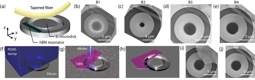
The hBN-Si cavity optomechanical systems studied here are shown in Figure 1 together with an overview of the fabrication process. The system consists of an hBN nanobeam suspended adjacent to 220 nm thick Si microdisk optical cavity. hBN-Si microdisks were fabricated on two different silicon chips for the studies presented here, with device B1 using an 8.4 diameter silicon microdisk, and devices B2 - B4 using 11.6 diameter microdisks. The dimensions of the hBN nanobeams fabricated in this work varied depending on the fabrication details described below, with the measured dimensions of each B1 - B5 given in the Supporting Information. Note that the reported hBN thickness is different for each device, and although not directly measured here, was estimated during the fabrication process to be less than approximately 50 nm for all of the devices, which is consistent with what is predicted from the nanomechanics measurements presented below. The hBN nanobeams are positioned between nm and from the microdisk edge depending on the device, as shown in Fig. 1(b – e) and in the Supporting Information. These gaps are small enough to observe fluctuations in the nanobeam position via the microdisk optical response. In the following, we assume that the hBN has a refractive index at the telecommunication band operating wavelength of the microdisk Cassabois, Valvin, and Gil (2016).
The microdisk fabrication process follows Ref. Borselli, Johnson, and Painter (2005), where they are first patterned in the Si layer of a silicon-on-insulator chip using electron beam lithography and reactive ion etching, followed by HF undercutting to remove the underlying of SiO2 until the microdisks are supported by thin SiO2 pedestals. The process for integrating an hBN mechanical resonator with the microdisk is summarized in Figs. 1(f - h). The electron beam lithography pattern used to define the microdisk creates a ring shaped trench surrounding the device over which an hBN nanobeam can be suspended. The first step in creating the nanobeam is to transfer an hBN flake with homogeneous thickness and high quality adjacent to the pre-fabricated microdisk using a dry PDMS stamp transfer technique (Fig. 1(f)). EBIE is then used to define a nanomechanical resonator separated by a small gap from the Si microdisk. During this process, a focused electron beam in the presence of water vapour induces selective chemical reactions with hBN, which leads to localized volatilization (Fig. 1(g)) Elbadawi et al. (2016). Since EBIE is entirely chemically driven, this process does not destroy the adjacent Si microdisk as evidenced by the SEM images in 1(b-e), and the high optical of the device presented below. Additionally, EBIE has not been observed to induce crystalline damage to the hBN nanobeam, compared to other methods such as focused ion beam milling Kim et al. (2018). For further illustration of the fabrication process, SEM images of a device before and after EBIE are shown in Fig. 1(i,j). For detailed before and after fabrication images of all the devices, see the Supporting Information. An advantage of this in-situ patterning technique is that it allows the gap between the nanobeam and the microdisk to be finely adjusted. This is of critical importance, as large gaps between hBN resonator and Si microdisk prevent observation of optomechanical coupling. While the serial nature of the etching process is not immediately scalable, it is well suited for studying this hBN-Si hybrid system as it is non invasive to the underlying silicon structure. It also allows prototyping devices, which are in turn used here for initial characterization of the nanomechanical properties of the hBN nanobeams with high sensitivity.
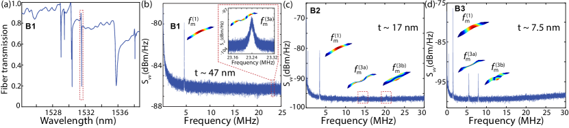
Measurement of the optomechanical properties of the hBN-Si system was achieved using a dimpled optical fiber taper to couple light into and out of the Si microdisk Michael et al. (2007). In order to reduce damping of the hBN nanobeam’s motion, measurements were performed in a vacuum chamber (base pressure, ), inside of which nanopositioners (Attocube) were used to position the device and the optical fiber taper. Figure 2(a) shows a typical transmission spectrum of the fiber taper when it placed in contact with the microdisk, evanescently coupling input light to it via a tunable laser (New Focus TLB-6700). Sharp dips in the transmission correspond to coupling to whispering gallery mode resonances of the microdisk, while broad low amplitude dips in transmission are related to wavelength dependent variations in the fiber taper transmission and laser output.
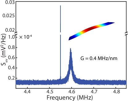
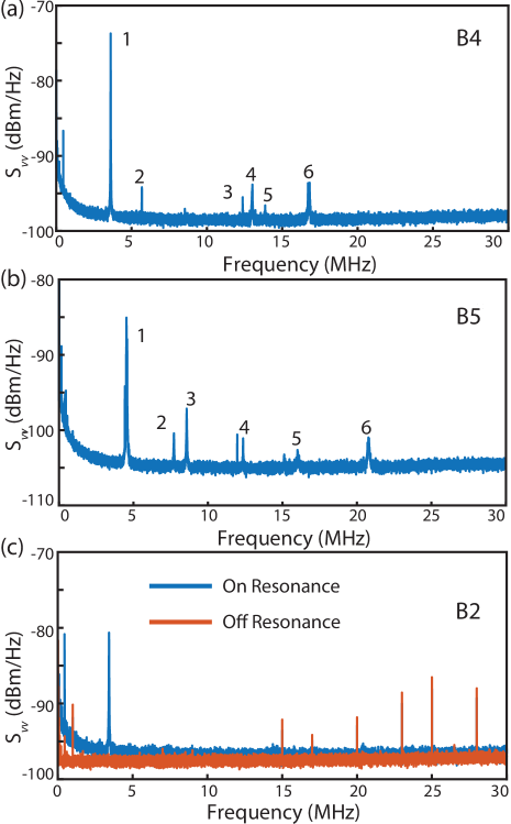
Mechanical motion of the nanobeam was probed by fixing the input laser wavelength within a high- resonance, and measuring the electronic power spectral density of the photoreceiver output (New Focus 1811) as in Ref. Wu et al. (2014). Typical spectra for multiple devices are shown in Fig. 2(b-d). For frequencies, MHz, these spectra are dominated by noise. However, peaks in the spectrum associated with thermally driven motion of normal mechanical modes of the hBN nanobeams are identifiable at higher frequencies. For example, in the case of the B1 device spectrum in Fig. 2(b), peaks with resonance frequencies and are visible. Based on Lorentzian fits, these resonances are observed to have linewidths corresponding to and , respectively. The high- optical resonance near used in this measurement is highlighted in Fig. 2(a), and found to have (see below) and dominant electric field polarization along the radial direction (TE –like). To improve the visibility of these nanobeam related peaks, after the study of device B1, devices B2 – B5 were fabricated with nominally smaller nanobeam-microdisk gaps. The smallest fabricated gaps, e.g. for device B3, was found to be below the 50 nm resolution of the SEM images taken during device fabrication. Higher resolution images were not taken to avoid damaging the hBN nanobeam. The spectra in Figs. 2(c) and (d) of devices B2 and B3, respectively, have a larger signal to noise as well as an additional third visible resonance. Table 1 summarizes the measured resonance frequencies and quality factors for devices B1 – B5.
| Device | (nm) | (MHz) | (MHz) | (MHz) | ||||
| B1 | 47 | 4.6 (4.6) | 23.24 (22.8) | - | 260 | 1100 | - | - |
| B2 | 17 | 3.42 (3.4) | 14.45 (14.3) | 20.4 (20.9) | 215 | 214 | 930 | 1.4 |
| B3 | 7.5 | 1.58 (1.6) | 5.56 (5.55) | 7.96 (8.1) | 278 | 224 | 298 | 1.4 |
| B4 | 18.5 | 3.54 (3.5) | 12.99 (13.0) | 16.8 (17.2) | 678 | 630 | 1098 | 1.3 |
| B5 | 51 | 4.6 (4.6) | 15.7 (15.5) | 20.8 (20.6) | 657 | 770 | 684 | 1.3 |
To better understand the nanomechanical nature of these resonances, finite element simulations (COMSOL) were used to calculate the normal mode spectrum of the nanobeams under study. These were then compared with the observed resonances, as shown in Table 1. This process is complicated somewhat by uncertainty in the thickness of each nanobeam stemming from lack of angled high resolution SEM images, and unwanted etching of the hBN nanobeam from EBIE, as described in the Supporting Information. Assuming a Young’s modulus of 865 GPa Falin et al. (2017), for a nanobeam thickness of 31 nm for device B1 we find good agreement between the observed resonances and predicted of 4.59 MHz and 23.24 MHz for the 1st () and 3rd () order vertical modes of the nanobeam, respectively. The simulated displacement profiles of these modes are shown in Fig. 2(b). Other studies have reported lower Young’s modulus, e.g. 392 GPa Zheng, Lee, and Feng (2017), which could be related to differences in material quality or the presence of internal compressive stress. Using this lower Young’s modulus in our simulations results in a predicted hBN thickness of 47 nm for device B1. This lower value of Young’s modulus is used throughout the remaining studies as the larger thickness is most consistent with the expected dimensions. Atomic force microscope measurements, combined with high resolution angled SEM images would provide more accurate characterization of the hBN thickness, and while not employed here to avoid risk of damaging the devices, will be useful in future studies to help reduce this ambiguity.
The order vertical mode of device B1 is not observed due to the odd symmetry of its displacement profile with respect to the -axis (defined in Fig. 1(a)) and the even symmetry of the microdisk mode intensity about this axis. As a result, the optomechanical coupling coefficient, , which predicts the shift in the frequency of the cavity mode for a given mechanical displacement , vanishes, resulting in nominally no cavity optomechanical transduction of the motion of this mode Schilling et al. (2016). The lowest order horizontal mechanical mode is predicted to have MHz for device B1, and was also not observed. This could be explained by its lower thermally driven amplitude () owing to its high frequency. Note that this effect is also responsible for the low observed amplitude of the peak.
As shown in Table 1, devices B2 and B3 are predicted by comparison to simulation to have thickness of 17 nm and 7.5 nm, respectively. The small thicknesses of B3 is in qualitative agreement with its SEM image in Fig. 1(d), in which the nanobeam is highly transparent. The additional 3rd resonance at frequency of devices B2 and B3 was also predicted by simulations, and originates from the asymmetry along the -axis of the hBN nanobeams studied here. The two resulting 3rd-order vertical modes, and , have maximum displacement on one each of the two long edges of the beam, as shown in Figs. 2(c-d)). This asymmetry arises due to the circular shape of the window over which the hBN nanobeams are clamped by van der Waals forces. The ratio was observed to be relatively constant across devices, as expected from analytic theory Brand et al. (2015). Measurements of device B1 were unable to resolve the mode, likely due to its relatively high frequency of 32.3 MHz and the poor signal to noise for this device. In order to find agreement between simulation and measured frequencies for device B3 it was necessary to include a 3 nm vertical curvature at the center of the beam. This curvature was not necessary for devices B1 and B2, and a larger curvature was necessary for B4 and B5 (see Supporting Information). This indicates that compressive stress may be present in these devices. Devices B4 and B5 also displayed additional resonances not explained by simulations and requiring further investigation in future work (see Supporting Information). Mechanical of the measured fundamental and higher order modes varied between 215 and 1100 for the measured devices, with no clear correlation between and device thickness. As hBN is a van der Waals material it may experience strong slipping between layers upon strainingKobayashi et al. (2017), which could in turn lead to variation in the observed mechanical properties. In this work only primarily macroscopic strain effects were considered, however this system could provide a useful platform for studying these nanoscopic effects.
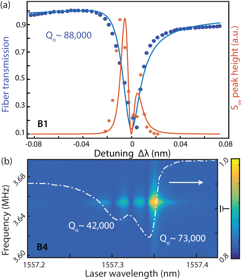
To better confirm that the peaks are related to optomechanically transduced hBN motion, their amplitudes were measured as a function of input laser detuning from the microdisk resonance wavelength . This is shown in Fig. 3(a) for the mode of device B1, from which we see that the peak amplitude follows the slope of the cavity optical response: , and that it is maximum when the laser is near the point of maximum slope. This behaviour is consistent with the sideband unresolved system studied here exhibiting predominantly dispersive optomechanical coupling between the hBN and the microdisk. Dominantly dispersive coupling is possible due to the low optical absorption of hBN at the operating wavelength, in contrast to the dissipative optomechanical coupling observed in highly absorbing graphene cavity optomechanical systems Cole et al. (2015), indicative of hBN’s suitability for cavity optomechanics. Note that the asymmetry in is well predicted from the asymmetry in the lineshape of the microdisk resonance, which arises from interference effects related to higher order modes of the fiber taper waveguide Wu et al. (2014) as well as small thermal instability in the microdisk Barclay, Srinivasan, and Painter (2005).
To further illustrate that the optomechanical coupling demonstrated here is primarily dispersive in nature, a spectrograph showing the wavelength dependence of the power spectral density was measured for the mode of device B4, as shown in Fig. 3(b). In this measurement an optical doublet mode corresponding to nearly degenerate standing wave modes created by backscattering in the microdisk Borselli, Johnson, and Painter (2005) was used, with for the symmetric mode and for anti-symmetric mode. As for the previous device, we observed that , with maxima when the laser wavelength is near the points of maximum slope for each mode of the doublet.
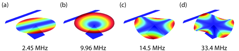
Several additional observations were used to confirm that the measurements described above are not related to normal modes of the microdisk itself. The lowest frequency microdisk mode with non-zero nominal optomechanical coupling is the radial breathing mode Mitchell, Hryciw, and Barclay (2014); Sun, Zhang, and Tang (2012), whose frequency is orders of magnitude higher than resonances observed here. Lower frequency mechanical modes of the microdisk can in principle have small non-zero optomechanical coupling resulting from asymmetries in device geometry. However, COMSOL simulations (see Supporting Information) of the B1 microdisk indicate that its lowest frequency modes are at 2.5 MHz, 9.9 MHz, 14.4 MHz and 33.4 MHz, which do not correspond to the observed resonances. Finally, all measurements were carried out with the fiber taper in contact with the microdisk, which should damp its mechanical motion significantly.
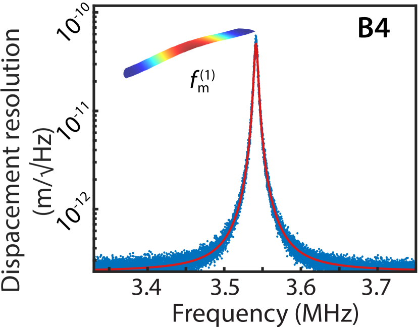
The measurement resolution of the cavity optomechanical system can be extracted from the measured signal to noise ratio of each thermomechanically driven peak using the expression , where , is Boltzmann’s contstant and is the device temperature Hauer et al. (2013); Wu et al. (2014). Here is defined by the ratio of the resonance peak height to the measurement noise floor, and is the predicted effective mass of the normal mode, as defined in Ref. Aspelmeyer, Kippenberg, and Marquardt (2014). From COMSOL simulations we find fg, fg, and fg for the , and modes of device B4, respectively, assuming an hBN density of 2100 kg/m3 Cartamil-Bueno et al. (2017); Rumyantsev et al. (2001). Note that this anomalous decrease in with mode order is related to the nanobeam’s non right-angle clamping points and resulting trapezoidal shape. From the data in Fig. 4, which was obtained with tuned to maximize the signal, we find , corresponding to fm/Hz1/2. This is smaller than comparable graphene cavity optomechanical systems Cole et al. (2015) but larger than what has been achieved in optomized SiN nanobeam cavity optomechanical device Schneider and Seidler (2016). Sensitivity could be further improved through operation at lower temperature, enhancements of to the level observed by Borselli et al. Borselli, Johnson, and Painter (2005), and as discussed below, increased . In addition, an input optical power, was used for these measurements, limited by the presence of thermally–induced optical shifts from two photon absorption in the Si microdisk Barclay, Srinivasan, and Painter (2005). As typically increases with Wu et al. (2014), improved measurement resolution could be achieved using a microdisk fabricated from a material which does not suffer from nonlinear absorption at nm and is compatible with the fabrication process, such as GaPMitchell, Hryciw, and Barclay (2014).
The optomechanical coupling affects the measurement resolution through , and can be optimized through the positioning of the nanobeam relative to the microdisk Schilling et al. (2016). To assess in our system, we implemented the calibration technique (see Supporting Information) from Refs. Gorodetksy et al. (2010); Schneider and Seidler (2016) which adds a known phase modulation to the input laser that is then transduced by the cavity into an optical intensity modulation. From the measured tone height relative to the area under nanomechanical resonance peak, we extracted MHz/nm for device B1. This is smaller than, but in reasonable agreement with, MHz/nm predicted from a perturbation theory calculations of the dependence of on the nanobeam height Schilling et al. (2016). This calculation was performed by evaluating the overlap of the microdisk mode intensity with the nanobeam dielectric, where finite difference time domain simulations (MEEP Oskooi et al. (2010)) were used to determine the azimuthaly symmetric field (fundamental TE-like mode, azimuthal number , travelling wave field distribution) of the unperturbed microdisk. This calculation does not take into account the local field correction to the microdisk field by the nanobeam Johnson et al. (2002), which may account for the discrepancy. Significant uncertainty can also arise from variation in the gap between the hBN nanobeam and the microdisk, as depends exponentially on this parameter Schilling et al. (2016).
After characterizing device B1, devices B2 - B5 were fabricated with a smaller gap in order to increase . While this is largely borne out by the larger signal to noise ratio of the spectra measured here, care must be taken to disentangle differences in from variations in , optical mode order, and microdisk and nanobeam dimensions. A systematic study of the influence of gap size on , and its effect on , is not undertaken here but is required in future work to fully optimize this system. However, the good agreement between the measured and predicted value of for B1 indicates that executing this optimization numerically is likely to yield valuable insight.
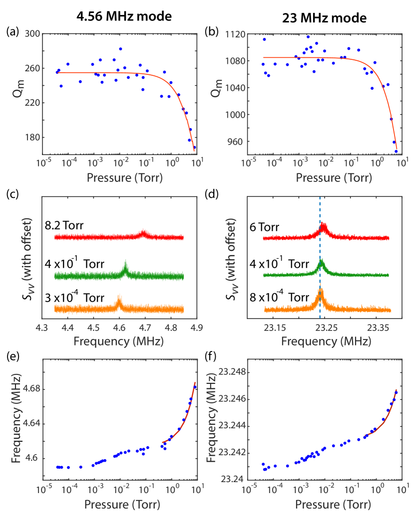
The properties of the hBN nanomechanical resonator were further probed by studying its dynamics as a function of vacuum pressure. Figures 5(a) and 5(b) show the observed dependence of for the and modes of device B1, respectively. In each case, is unaffected by pressure for , taking a constant value in this pressure range. This indicates that air damping is not limiting for the measurements reported above. At higher pressure, as shown by the fits in Figs. 5(a-b), the pressure dependence of was well modeled by , where describes the influence of free molecular flow damping Blom et al. (1992); Verbridge et al. (2008); Lee et al. (2014). Note that the relatively similar pressures at which of the and modes begin to degrade is in agreement with the analytically predicted dependence of on mode frequency Verbridge et al. (2008); Lee et al. (2014).
The mechanical frequencies of the hBN nanomechanical resonators were also observed to change with , as shown in Figs. 5(c) and 5(d). This pressure dependent shift can be caused by several mechanisms. For , the shift follows . This behaviour is consistent with a squeeze film spring effect observed in nanomechanical resonators when the oscillation period is smaller than the response time of the gas molecules trapped between the resonator and the substrate Dolleman et al. (2015). This effect requires that the air mean free path is sufficiently small for molecules to fill the gap between the resonator and the substrate. However, at the mean free path of air is , which is larger than the maximum dimension () of the aperture defined by the gap between the nanobeam and substrate in device B1. This suggests that the vacuum chamber pressure in the vicinity of the device may be larger than measured by the pressure gauge, which is located near the turbo pump used to evacuate the chamber. Note that the chamber used here is a Montana Instruments Nanoscale Workstation nominally designed for low temperature operation.
Below the frequencies of both modes also increase with pressure, although with a different pressure dependence. Similar behavior was observed by Lee et al. where it was ascribed to stress induced by the local pressure differential experienced by the nanobeam caused due to restriction of air molecules from entering the volume between the nanobeam and the underlying silicon chip Lee et al. (2014), though other studies suggest that a steady state pressure should be reached Dolleman et al. (2016). Finally, note that optical power dependent measurements of confirmed that local photothermal heating was not influencing the results reported here, as described in the Supporting Information.
Note that for the measurement in Fig. 5(c,d) a different optical mode, at 1489.7 nm (), was used than in other measurements of device B1. This optical mode had improved transduction for the mechanical mode at the expense of smaller transduction for the first order mechanical mode, allowing measurement of small frequency shifts of the third order mode. This change in relative transduction strength is possibly related to differences in optical mode order, which affects the optical field overlap with the nanobeam.
To conclude, we have experimentally demonstrated an hBN cavity optomechanical system with displacement sensitivity fm/Hz1/2, and have shown that hBN nanobeams support mechanical resonances with exceeding 1000 at 23 MHz frequency in room temperature vacuum conditions. Our results are the first step towards integration of hBN as vital component of an integrated quantum optomechanical systems. Within the context of spin-optomechanics, future studies will examine whether optomechanical control of hBN nanomechanical resonators can be used to modify the emission properties of hBN emitters. Future research will also examine whether novel or enhanced optical forces resulting from the hyperbolic nature of hBN can be demonstrated. While the hBN-Si system presented here would be unsuitable for collection of single photon emission from hBN or studying hBN’s optomechanical properties in the lower Restrahlen band due to silicon’s optical absorption at those wavelength, this Si system could be used for studying optomechanics in the upper Restrahlen band. Furthermore, the flexibility of the fabrication process described in this work would allow integration of the hBN structures with microdisks fabricated from materials who do not suffer absorption at these wavelengths, such as GaP Mitchell, Hryciw, and Barclay (2014), which would allow the study of the single photon emitters present in hBN.
In the immediate future, experiments will be focused on optimizing the design of the hBN nanomechanical resonator and its integration with the optical cavity, fabricating optomechanical crystals Eichenfield et al. (2009) directly from hBN and implementation of other fully integrated hBN cavity optomechanical devices, and measurement of hBN nanomechanical properties at cryogenic temperatures. Such experiments would provide additional insight into the nanomechanical properties of hBN resonators and their interaction with optical fields, and allow development sub-fm/ readout of hBN resonator motion Schneider and Seidler (2016).
Acknowledgments We thank the referees and R. Dolleman for their helpful comments. Financial support from the Australian Research council (via DP180100077, LP170100150), the Asian Office of Aerospace Research and Development grant FA2386-17-1-4064, the Office of Naval Research Global under grant number N62909-18-1-2025, the Natural Science and Engineering Research Council, and the National Research Council are gratefully acknowledged.
References
- Kippenberg and Vahala (2007) T. Kippenberg and K. Vahala, Opt. Express 15, 17172 (2007).
- Aspelmeyer, Kippenberg, and Marquardt (2014) M. Aspelmeyer, T. J. Kippenberg, and F. Marquardt, Rev. Mod. Phys. 86, 1391 (2014).
- Chan et al. (2011) J. Chan, T. P. M. Alegre, A. H. Safavi-Naeini, J. T. Hill, A. Krause, S. Groblacher, M. Aspelmeyer, and O. Painter, Nature 478, 89 (2011).
- Teufel et al. (2011) J. Teufel, T. Donner, D. Li, J. Harlow, M. Allman, K. Cicak, A. Sirois, J. D. Whittaker, K. Lehnert, and R. W. Simmonds, Nature 475, 359 (2011).
- Schliesser et al. (2009) A. Schliesser, O. Arcizet, R. Rivière, G. Anetsberger, and T. Kippenberg, Nature Phys. 5, 509 (2009).
- Cohen et al. (2015) J. D. Cohen, S. M. Meenehan, G. S. MacCabe, S. Gröblacher, A. H. Safavi-Naeini, F. Marsili, M. D. Shaw, and O. Painter, Nature 520, 522 (2015).
- Purdy et al. (2017) T. P. Purdy, K. E. Grutter, K. Srinivasan, and J. M. Taylor, Science 356, 1265 (2017).
- Sudhir et al. (2017) V. Sudhir, R. Schilling, S. A. Fedorov, H. Schütz, D. J. Wilson, and T. J. Kippenberg, Phys. Rev. X 7, 031055 (2017).
- Hong et al. (2017) S. Hong, R. Riedinger, I. Marinković, A. Wallucks, S. G. Hofer, R. A. Norte, M. Aspelmeyer, and S. Gröblacher, Science 358, 203 (2017).
- Anetsberger et al. (2009) G. Anetsberger, O. Arcizet, Q. Unterreithmeier, R. Riviere, A. Schliesser, E. Weig, J. Kotthaus, and T. Kippenberg, Nature Phys. 5, 909 (2009).
- Srinivasan et al. (2011) K. Srinivasan, H. Miao, M. Rakher, M. Davanço, and V. Aksyuk, Nano Lett. 11, 791 (2011).
- Kim et al. (2013) P. Kim, C. Doolin, B. Hauer, A. MacDonald, M. Freeman, P. Barclay, and J. Davis, Appl. Phys. Lett. 102, 053102 (2013).
- Forstner et al. (2012) S. Forstner, S. Prams, J. Knittel, E. van Ooijen, J. Swaim, G. Harris, A. Szorkovszky, W. Bowen, and H. Rubinsztein-Dunlop, Phys. Rev. Lett. 108, 120801 (2012).
- Yu et al. (2015) W. Yu, W. C. Jiang, Q. Lin, and T. Lu, arXiv:1504.03727 (2015).
- Schilling et al. (2016) R. Schilling, H. Schütz, A. H. Ghadimi, V. Sudhir, D. J. Wilson, and T. J. Kippenberg, Phys. Rev. Applied 5, 054019 (2016).
- Wu et al. (2017) M. Wu, N. L.-Y. Wu, T. Firdous, F. F. Sani, J. E. Losby, M. R. Freeman, and P. E. Barclay, Nature nanotechnology 12, 127 (2017).
- Fiore et al. (2011) V. Fiore, Y. Yang, M. C. Kuzyk, R. Barbour, L. Tian, and H. Wang, Physical review letters 107, 133601 (2011).
- Hill et al. (2012) J. T. Hill, A. H. Safavi-Naeini, J. Chan, and O. Painter, Nat. Commun. 3, 1196 (2012).
- Liu et al. (2013) Y. Liu, M. Davanço, V. Aksyuk, and K. Srinivasan, Phys. Rev. Lett. 110, 223603 (2013).
- Fang et al. (2017) K. Fang, J. Luo, A. Metelmann, M. H. Matheny, F. Marquardt, A. A. Clerk, and O. Painter, Nature Physics 13, 465 (2017).
- Ruesink et al. (2018) F. Ruesink, J. P. Mathew, M.-A. Miri, A. Alù, and E. Verhagen, Nature communications 9, 1798 (2018).
- Cole et al. (2015) R. M. Cole, G. A. Brawley, V. P. Adiga, R. De Alba, J. M. Parpia, B. Ilic, H. G. Craighead, and W. P. Bowen, Physical Review Applied 3, 024004 (2015).
- Song et al. (2014) X. Song, M. Oksanen, J. Li, P. J. Hakonen, and M. A. Sillanpää, Physical review letters 113, 027404 (2014).
- Ekinci, Yang, and Roukes (2004) K. Ekinci, Y. Yang, and M. Roukes, Journal of applied physics 95, 2682 (2004).
- Gil-Santos et al. (2015) E. Gil-Santos, C. Baker, D. Nguyen, W. Hease, C. Gomez, A. Lemaître, S. Ducci, G. Leo, and I. Favero, Nature nanotechnology 10, 810 (2015).
- Roy et al. (2018) S. K. Roy, V. T. Sauer, J. N. Westwood-Bachman, A. Venkatasubramanian, and W. K. Hiebert, Science 360, eaar5220 (2018).
- Tran et al. (2016) T. T. Tran, K. Bray, M. J. Ford, M. Toth, and I. Aharonovich, Nature nanotechnology 11, 37 (2016).
- Xia et al. (2014) F. Xia, H. Wang, D. Xiao, M. Dubey, and A. Ramasubramaniam, Nature Photonics 8, 899 (2014).
- Caldwell et al. (2014) J. D. Caldwell, A. V. Kretinin, Y. Chen, V. Giannini, M. M. Fogler, Y. Francescato, C. T. Ellis, J. G. Tischler, C. R. Woods, A. J. Giles, M. Hong, K. Watanabe, T. Taniguchi, S. A. Maier, and K. S. Novoselov, Nature communications 5, 5221 (2014).
- Dai et al. (2014) S. Dai, Z. Fei, Q. Ma, A. Rodin, M. Wagner, A. McLeod, M. Liu, W. Gannett, W. Regan, K. Watanabe, T. Taniguchi, M. Thiemens, G. Dominguez, A. H. Castro Neto, A. Zettl, F. Keilmann, P. Jarillo-Herrero, M. M. Fogler, and D. N. Basov, Science 343, 1125 (2014).
- He et al. (2012) Y. He, S. He, J. Gao, and X. Yang, Opt. Express 20, 22372 (2012).
- Exarhos et al. (2017) A. L. Exarhos, D. A. Hopper, R. R. Grote, A. Alkauskas, and L. C. Bassett, ACS nano 11, 3328 (2017).
- Jungwirth et al. (2016) N. R. Jungwirth, B. Calderon, Y. Ji, M. G. Spencer, M. E. Flatté, and G. D. Fuchs, Nano letters 16, 6052 (2016).
- Abdi et al. (2017) M. Abdi, M.-J. Hwang, M. Aghtar, and M. B. Plenio, Physical review letters 119, 233602 (2017).
- Cassabois, Valvin, and Gil (2016) G. Cassabois, P. Valvin, and B. Gil, Nature Photonics 10, 262 (2016).
- Li and Chen (2016) L. H. Li and Y. Chen, Advanced Functional Materials 26, 2594 (2016).
- Falin et al. (2017) A. Falin, Q. Cai, E. J. Santos, D. Scullion, D. Qian, R. Zhang, Z. Yang, S. Huang, K. Watanabe, T. Taniguchi, M. R. Barnett, Y. Chen, R. S. Ruoff, and L. H. Li, Nature communications 8, 15815 (2017).
- Zheng, Lee, and Feng (2017) X.-Q. Zheng, J. Lee, and P. X.-L. Feng, Microsystems & Nanoengineering 3, 17038 (2017).
- Elbadawi et al. (2016) C. Elbadawi, T. T. Tran, M. Kolíal, T. Šikola, J. Scott, Q. Cai, L. H. Li, T. Taniguchi, K. Watanabe, M. Toth, I. Aharonovich, and C. Lobo, Nanoscale 8, 16182 (2016).
- Kim et al. (2018) S. Kim, J. E. Fröch, J. Christian, M. Straw, J. Bishop, D. Totonjian, K. Watanabe, T. Taniguchi, M. Toth, and I. Aharonovich, Nature communications 9, 2623 (2018).
- Castellanos-Gomez et al. (2015) A. Castellanos-Gomez, V. Singh, H. S. van der Zant, and G. A. Steele, Annalen der Physik 527, 27 (2015).
- Cartamil-Bueno et al. (2017) S. J. Cartamil-Bueno, M. Cavalieri, R. Wang, S. Houri, S. Hofmann, and H. S. van der Zant, npj 2D Materials and Applications 1, 16 (2017).
- Borselli, Johnson, and Painter (2005) M. Borselli, T. J. Johnson, and O. Painter, Opt. Express 13, 1515 (2005).
- Michael et al. (2007) C. P. Michael, M. Borselli, T. J. Johnson, C. Chrystala, and O. Painter, Opt. Express 15, 4745 (2007).
- Wu et al. (2014) M. Wu, A. C. Hryciw, C. Healey, D. P. Lake, M. R. Freeman, J. P. Davis, and P. E. Barclay, Phys. Rev. X 4, 021052 (2014).
- Brand et al. (2015) O. Brand, I. Dufor, S. Heinrich, F. Josse, G. K. Fedder, C. Hierold, J. G. Korvink, and O. Tabata, eds., Resonant MEMS: Fundamentals, Implementation and Application (Wiley VCH Verlag GmbH & Co. KGaA, 2015).
- Kobayashi et al. (2017) Y. Kobayashi, T. Taniguchi, K. Watanabe, Y. Maniwa, and Y. Miyata, Applied Physics Express 10, 045201 (2017).
- Barclay, Srinivasan, and Painter (2005) P. E. Barclay, K. Srinivasan, and O. Painter, Opt. Express 13, 801 (2005).
- Mitchell, Hryciw, and Barclay (2014) M. Mitchell, A. C. Hryciw, and P. E. Barclay, Appl. Phys. Lett. 104, 141104 (2014).
- Sun, Zhang, and Tang (2012) X. Sun, X. Zhang, and H. X. Tang, Appl. Phys. Lett. 100, 173116 (2012).
- Hauer et al. (2013) B. D. Hauer, C. Doolin, K. S. D. Beach, and J. P. Davis, Annals of Physics 339, 181 (2013).
- Rumyantsev et al. (2001) S. Rumyantsev, M. Levinshtein, A. Jackson, S. Mohammad, G. Harris, M. Spencer, and M. Shur, Properties of Advanced Semiconductor Materials GaN, AlN, InN, BN, SiC, SiGe , 67 (2001).
- Schneider and Seidler (2016) K. Schneider and P. Seidler, Optics express 24, 13850 (2016).
- Gorodetksy et al. (2010) M. Gorodetksy, A. Schliesser, G. Anetsberger, S. Deleglise, and T. J. Kippenberg, Optics express 18, 23236 (2010).
- Oskooi et al. (2010) A. F. Oskooi, D. Roundy, M. Ibanescu, P. Bermel, J. Joannopoulos, and S. G. Johnson, Comp. Phys. Comm. 181, 687 (2010).
- Johnson et al. (2002) S. G. Johnson, M. Ibanescu, M. A. Skorobogatiy, O. Weisberg, J. D. Joannopoulos, and Y. Fink, Phys. Rev. E 65, 066611 (2002).
- Blom et al. (1992) F. Blom, S. Bouwstra, M. Elwenspoek, and J. Fluitman, Journal of Vacuum Science & Technology B: Microelectronics and Nanometer Structures Processing, Measurement, and Phenomena 10, 19 (1992).
- Verbridge et al. (2008) S. S. Verbridge, R. Ilic, H. Craighead, and J. M. Parpia, Applied Physics Letters 93, 013101 (2008).
- Lee et al. (2014) J. Lee, Z. Wang, K. He, J. Shan, and P. X.-L. Feng, Applied Physics Letters 105, 023104 (2014).
- Dolleman et al. (2015) R. J. Dolleman, D. Davidovikj, S. J. Cartamil-Bueno, H. S. van der Zant, and P. G. Steeneken, Nano letters 16, 568 (2015).
- Dolleman et al. (2016) R. J. Dolleman, S. J. Cartamil-Bueno, H. S. van der Zant, and P. G. Steeneken, 2D Materials 4, 011002 (2016).
- Eichenfield et al. (2009) M. Eichenfield, J. Chan, R. Camacho, K. Vahala, and O. Painter, Nature 462, 78 (2009).
Supplementary Information
.1 Fabrication & estimated device dimensions
Figure S1 shows optical and scanning electron micrographs (SEM) before and after electron beam induced etching (EBIE) process for all of the devices studied in this work. We note that the colour change of the hBN flake in the optical microscope images is associated with undesired etching in areas that are not directly exposed, as well as positioning the area of interest in the center of the electron beam, which will etch the surface layer ref:supp_elbadawi2016electron . This can potentially be bypassed by operating at lower electron beam energy, giving a smaller radius of backscattered electrons, which at this stage is a technical limitation.
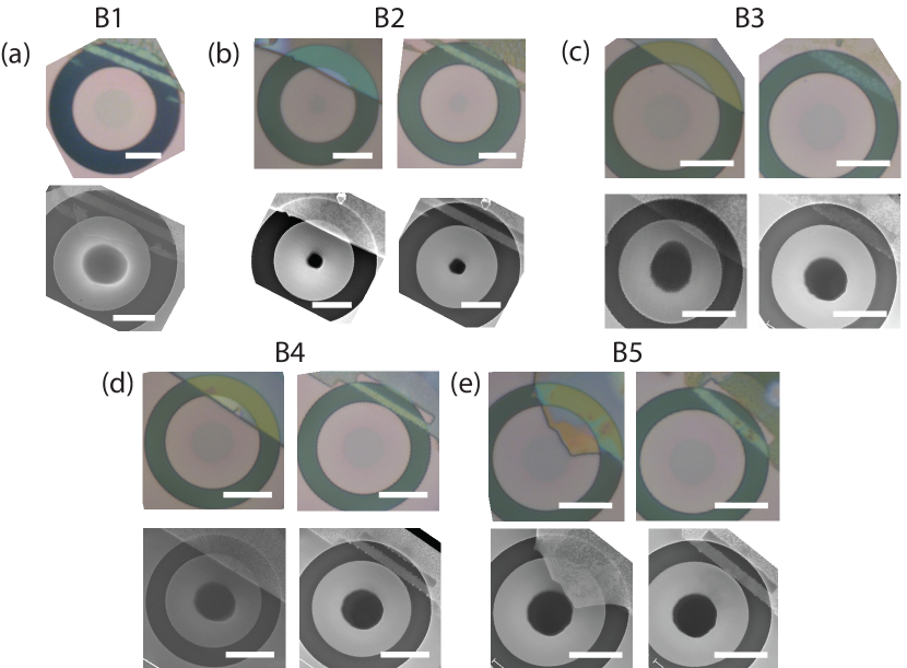
Table S1 gives the estimated dimensions for all devices studied in this work. The hBN beam length, , and width, were measured from SEM images, while the thickness was estimated by tuning it to match the simulated and measured mode frequencies, . Note that for devices B3-B5, a vertical curvature with height () had to be introduced to find good agreement with the measured mechanical modes, indicating that compressive stress may be present in these devices.
| Device | (m) | (m) | (nm) | (nm) | (MHz) | (MHz) | (MHz) |
| B1 | 13.5 | 1.1 | 47 | 0 | 4.6 | 22.8 | 32.3 |
| B2 | 10.04 | 0.92 | 17 | 0 | 3.4 | 14.3 | 20.9 |
| B3 | 12.7 | 1.6 | 7.5 | 3 | 1.6 | 5.55 | 8.1 |
| B4 | 11.4 | 1.15 | 18.5 | 9 | 3.5 | 13.0 | 17.2 |
| B5 | 13.4 | 1.08 | 51 | 20 | 4.6 | 15.5 | 20.6 |
.2 Microdisk mechanical normal modes
To rule out the presence of mechanical modes of the microdisk in the measured power spectral density, , the microdisk normal modes were simulated in COMSOL, using a disk thickness of 220 nm defined by the silicon on insulator material, and SEM measured diameter of 11.6 m. The lowest order modes which could have small non-zero optomechanical coupling resulting from asymmetries in device geometry are shown in Figure S2. As they are spectrally separated from the expected hBN nanobeam modes, and the fiber taper induced damping of its motion should be significant, we conclude that we do not observe these modes in our measured spectra.
.3 Power dependence of
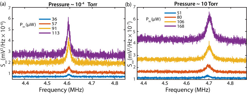
To rule out the shift in mechanical frequency due to local photothermal heating we studied the dependence of the measured power spectral density, , of the mode on input optical power, . As shown in Figures S3(a) and S3(b) the frequency of the mode of device B1 was observed to remain constant with increasing , for chamber pressures of and Torr, respectively.
.4 Optomechanical coupling coefficient calibration
To assess the optomechanical coupling coefficient, ref:supp_aspelmeyer2014co , in our system, we implemented the calibration technique developed in Ref. ref:supp_gorodetksy2010dvo which adds a known phase modulation to the input laser that is then transduced by the cavity into an optical intensity modulation. From the measured area under the modulation tone relative to the area under nanomechanical resonance peak shown in Figure S4 we extracted MHz/nm for device B1. This phase tone was created by passing the input laser through a electro–optic phase modulator (EOSpace) modulated at a frequency close to .
.5 Additional spectra and background noise removal
Wide band measurements of for device B4, and device B5 (not discussed in the main text) is shown in Figure S5(a,b) where, as in the main text, these measurements were carried out in vacuum (base pressure, P Torr), with the same methods described in the main text. For devices B4 and B5, we observed hybridization of certain modes which would exhibit multiple peaks in a narrow–band about the expected center frequency. A potential reason for this hybridization could be asymmetry present in the nanobeam due to thickness variations from EBIE and non-rectangular clamping areas at each end of the nanobeam and will be studied in future work.
To remove spurious noise features in resulting from electronic noise in our measurement apparatus a spectra was taken when the laser was placed off– resonance with the optical mode of the Si microdisk, while the fiber was parked. By comparing this off–resonance spectra to that when on–resonance, noise features were identified and removed from the spectra presented in the main text and and Figure S5(a,b).
References
- (1) C. Elbadawi, T. T. Tran, M. Kolíal, T. Sikola, J. Scott, Q. Cai, L. H. Li, T. Taniguchi, K. Watanabe, M. Toth, I. Aharonovich, and C. Lobo, Nanoscale 8 16182 (2016).
- (2) M. Aspelmeyer, T. J. Kippenberg, and F. Marquardt, Rev. Mod. Phys. 86, 1391 (2014).
- (3) M. Gorodetksy, A. Schliesser, G. Anetsberger, S. Deleglise, and T.J. Kippenberg, Optics express 18, 23236 (2010).