Yu-Shiba-Rusinov bound states versus topological edge states in Pb/Si(111)
Abstract
There is presently a tremendous activity around the field of topological superconductivity and Majorana fermions. Among the many questions raised, it has become increasingly important to establish the topological or non-topological origin of features associated with Majorana fermions such as zero-bias peaks. Here, we compare in-gap features associated either with isolated magnetic impurities or with magnetic clusters strongly coupled to the atomically thin superconductor Pb/Si(111). We study this system by means of scanning tunneling microscopy and spectroscopy (STM/STS). We take advantage of the fact that the Pb/Si(111) monolayer can exist either in a crystal-ordered phase or in an incommensurate disordered phase to compare the observed spectroscopic features in both phases. This allows us to demonstrate that the strongly resolved in-gap states we found around the magnetic clusters in the disordered phase of Pb have a clear topological origin.
1 Introduction
The pursuit of convincing clear signatures of Majorana fermions is at the center of the attention of the condensed matter community. There exists a vivid debate liu2018 ; mourik2012 ; nadjperge2014 about whether the observed zero-bias signatures measured in nanowires emerge from actual topologically protected objects or from trivial Shiba or Andreev bound states liu2018 .
Scanning tunneling microscopy and spectroscopy (STM/STS) techniques offer one of the most complete approach when it comes to investigate electronic behaviors. This experimental technique allows probing the local density of states at surfaces with an atomic resolution. As any technique, it also has its own inconveniences as it requires a conducting substrate and is restricted to systems with clean surfaces. Hence, many interesting systems studied by mesoscopic transport cannot be accessed by STM. For instance, systems such as semiconducting nanowires proximitized with a superconducting capping, from which possible signatures of Majorana fermions were first observed mourik2012 are difficult to study using this method. On the other hand, atomically thin superconductors such as Pb/Si(111) zhang2010 ; brun2014 ; brun2017 are perfectly suited since the intrinsic bidimensional aspect of these systems allows probing the whole material.
In this paper we describe and compare two different types of in-gap features observed in Pb/Si(111). The first features are Yu-Shiba-Rusinov (YSR) bound states yu1965 ; shiba1968 ; rusinov1969 induced by individual magnetic atoms. We discuss the effect of such local perturbation on the 2D superconducting electrons for two different phases of Pb/Si(111) monolayers: the phase and the stripped incommensurate (SIC) phases zhang2010 ; brun2014 . We will then focus on a new kind of in-gap edge states we found recently around magnetic Co clusters embedded below the Pb monolayers (first studied in menard2017 , see also bjornson2017 ).
2 Yu-Shiba-Rusinov bound states
Magnetic impurities in a superconducting substrate give rise to YSR bound states. It has been shown experimentally that the amplitude of the YSR bound states wave function depends on the dimensionality of the substrate menard2015 ; ruby16 ; choi17 . The wave function of YSR bound states is quite complex as it includes an oscillatory term at the scale of the Fermi wavelength convoluted by an envelope term with an exponential decay at the scale of the coherence legnth times an algebraic decay that depends on dimensionality. In two dimensions (2D) the algebraic decay is as while in 3D it follows a law. As STS is sensitive to the density of states and thus to the square modulus of the wave function, an algebraic decay of the Shiba states in is expected in 3D and in in 2D. This difference may seem negligible but in practice it has some spectacular consequences. In the first STM measurements of YSR states around individual impurities in 3D systems, the wave function was vanishing extremely rapidly (less than 1 nm) with the distance to the impurities yazdani1997 ; ji2008 and no spatial oscillations of the YSR states could be measured. We recently analyze the effect of magnetic impurities in 2H-NbSe2, a material with a 2D electronic structure, and were able to visualize the complex spatial structure of the wave function of YSR bound states menard2015 . A six-fold star shape pattern with branches that extend up to 8 nm from the impurities was observed and electron-hole oscillations with a period given by the Fermi wavelength was observed as predicted by Rusinov in 1969 rusinov1969 . Since this work, similar complex YSR pattern were also observed in 3D materials such as Pb(111) and Pb(100) in which the spatial extend was found smaller. However, even in 3D materials the YSR states can extend quite far in certain directions due to a kind of channeling effect related to the anisotropy of the Fermi surface: in certain location, the Fermi surface can be 2D-like, which leads to some longer-range Shiba states in these particular directions ruby16 .
2.1 Spectroscopic characteristics
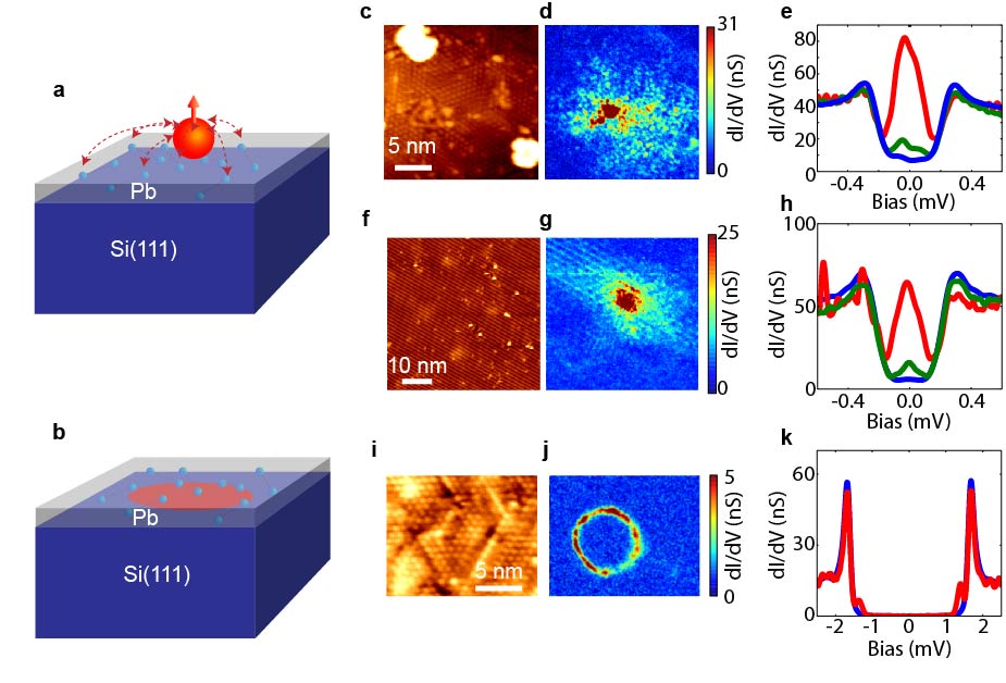
The schematic view of the system we consider is sketched in fig. 1.a. In Figs 1.c and 1.f we present the topography of two areas belonging respectively to the SIC and phases of Pb/Si(111). The SIC phase appears as an isotropic disordered surface reconstruction while the appears as domains containing stripes that can exist in three different orientations. Fig. 1.f shows one orientational domain. Two other orientations rotated by 60∘ and 120∘ are also measured on other locations of the sample. Figs 1.d and 1.g show conductance maps integrated in bias between -0.2 mV and 0.2 mV. For these two maps a central impurity can be seen (high conductance, red color, colors online) from which emerges a real space conductance pattern. For both samples, the impurities are native to the Pb source used for the growth and, though unidentified, is most probably Fe, Co or Cr (possible pollutants in our triple e-beam evaporator used for Pb deposition).
A YSR bound state gives rise to a pair of in-gap states in the superconducting spectra. Such YSR states measured in Pb monolayers are shown on Figs 1.e for the SIC phase and on 1.h for the phase. In both cases we present a selection of three spectra taken on the impurity site (red), 5 nm away from the impurity (green) and far from the impurity (blue). For the SIC spectra shown in Fig. 1.e, we can observe a pair of very intense peaks whose amplitude diminishes as we move away from the center of the impurity. In the case of the , a strong peak at zero-bias, with a slight shoulder at positive energy, is observed whose amplitude also decreases when moving away from the center of the impurity. The difference in energy position of these states is easily explained by looking at the equation giving the energy of the YSR bound states menard2015 . The energy of the YSR states involves both the magnetic exchange interaction and the scattering potential. Therefore, the exact position of the in-gap states depends on the position in the crystal and its chemical nature and may vary a lot between samples. However, one feature that is everlasting is that the energy position of the YSR states we observe in STS do not vary as function to the distance to the impurities. No energy dispersion is measured, one impurity will give rise to one (or a few ji2008 ; ruby16 , depending on crystal field effects) peak at a given energy.

2.2 Spatial pattern
Let us now turn our attention to the spatial structure of the YSR pattern in the conductance maps. For the ordered we see that the YSR bound state spatial pattern follows the symmetry of the underlying crystal and forms lines in the same direction as the atomic raws observed in the topography. This pattern can be directly related to the Fermi surface of the material shown in Fig. 2 kim2010 , the quasiparticle interferences (QPI) occurring along well defined axes described in figs. 1.a-c. The particular scattering channel depicted on Fig. 1.b leads to a YSR pattern with exactly twice the atomic periodicity of the atomic lattice. This expected structure is in perfect agreement with the measurements.
In stark contrast with this case, the SIC phase exhibits a YSR bound state whose spatial behavior is speckle-like. This finds its origin in the disordered nature of the incommensurate Pb layer which does not benefit from a well defined Fermi surface and thus randomizes the QPI. The only relevant scale in this case is the typical atomic distance that fixes the size of the spots from the speckle pattern. The role of disorder is thus made clear in the context of YSR bound states in which no long range ordered structure are expected to appear in the case of a disordered superconductor except if some underlying mechanism, such as a topological protection, prevents against scattering.
3 Topological superconductivity
One of the reason why topology gets so much attention in condensed matter physics is due to the so called topological protection. This means that some kinds of local perturbations of a topological system will leave the system essentially unaltered. In the context of Pb/Si(111) disordered SIC phase, this means that only topologically protected features will be observable as coherent objects at scales for which YSR are observed as speckle pattern, i.e. at scales larger that the interatomic distances.
One way to obtain such protected states is to use a local Zeeman field in order to induce a topological transition in a Rashba superconductor, such as a Pb monolayer. We have recently studied this kind of device and we found that it indeed leads to some clear hint of a topological transition menard2017 . The system studied is based on the SIC phase described above except that a very small amount of Co was deposited on Si(111) prior to the deposition of the Pb layer. This intermediate step, followed by an annealing at around 375∘C, leads to a clusturization of the Co atoms into Si-Co domains located just below the Pb monolayer. By this process one get insulating magnetic clusters of sizes ranging from 5 to 40 nm that provokes a strong magnetic exchange field into the superconducting Pb monolayer. The geometry of the samples is presented in Fig. 1.b as a schematic view. The topography of the sample is shown on Fig. 1.i and the corresponding zero energy conductance map is shown on Fig.1.j. Note that in order to get a higher energy resolution a superconducting Pb tip was used for this measurement while for the Shiba states discussed above a normal Pt tip was used (in all the cases the measurement were performed at 300 mK). Therefore, the conductance map at zero energy shown in fig.1.j was measured at a tunnel bias shifted by the tip gap meV (the precise methodology used for the deconvolution of the tip DOS is detailed in ref. menard2017 ). The most intriguing feature of fig.1.j is that a very regular edge state is observed, it appears as an almost circular ring of thickness 0.7 nm. This is in striking contrast with the conductance map of YSR bound states around a magnetic impurity observed in the same SIC Pb/Si(111) monolayer (fig. 1.d) which exhibits a speckle like pattern.

In Fig. 3 we present yet another example of edge states observed experimentally in a sample different from the one presented in Fig. 1.i. In this configuration we recover the same basic characteristic states crossing the superconducting gap. The underlying Co cluster here is elongated while the one from Fig. 1.i is almost circular. As a result, the edge states we image elongated as well.
In order to put aside any suspicion of tip related artifacts, we present in Fig. 4 yet another example of this kind of edge state acquired with a normal tip, in the exact same condition as for the YSR bound states we first described in Fig. 1. Once again, the sharp ring is observed with an associated dispersion presented in Fig. 4.f.

4 Theoretical description
4.1 Model Hamiltonian
On the theory level, YSR bound states and topological edge states are both associated with magnetic inhomogeneities, however of different size. In order to describe qualitatively the observed features, we rely on symmetry to build an effective phenomenological Hamiltonian. Pb/Si(111) breaks inversion symmetry and has therefore a strong Rashba spin orbit coupling. Moreover, most of the electronic spectrum is dominated by the band around the point in the Brillouin zone. Combining these two features, we proposed in menard2017 the following Boguliubov de-Gennes (BdG) Hamiltonian:
| (1) |
In Eq. (1), is the band dispersion near the point; and (with ) are Pauli matrices acting in the particle hole and the spin space respectively. is the Zeeman splitting term and we define . Because inversion symmetry is broken, the superconducting order parameter will also contain a triplet component rashba together with the usual singlet component . We therefore need to obtain the eigen-energies of , with the Nambu basis spinor given by .
The difference between a Shiba bound state and a topological edge state resides in the definition of . A Shiba bound state appears for a very localized potential such as , while a potential extending over distance much larger than the atomic size can lead to a local topological transition menard2017 . The experimental results shown in figures 1.j and 4 were obtained with magnetic clusters with diameters of roughly 10 nm, which is much larger than the atomic length scale but smaller than the coherence length nm.
In order to simplify the discussion let us first consider a spatially invariant configuration (infinite magnetic cluster) to study the topological properties of the Hamiltonian Eq. (1) for different configurations of the parameters. In a translationally invariant case (for ), the 44 matrix defined in Eq. (1) can easily be diagonalized in order to obtain the eigen-energies of the system. We find four solutions, two electron-like and two hole-like with symmetric energies with respect to the Fermi level. These are given by the following expression
| (2) |

From this dispersion relation it becomes possible to compute the points at which the gap will close (when the system actually undergoes a topological transition) before reopening as a function of the different parameters. Figures 5.b and 5.d present two phase diagrams calculated in the limits and respectively.
In the first case (), the dispersion in Eq. (2) can be simplifed into
| (3) |
from which we can observe a topological transition from a trivial superconductor to a chiral one at a critical field where the gap closes at (see Fig. 5.a). It is worth noting here that even though the spin-orbit coupling does not explicitly intervene in the expression of the critical field, its presence is absolutely necessary to guarantee the reopening of the gap at larger fields. It is easily seen that for , the gap does not reopen and thus prevents the appearance of a gapped topological superconducting phase.
The second case shown in Fig. 5 corresponds to the condition and for which the superconductor is time-reversal invariant, and we expect a transition from a trivial to a helical state. In this case, the topological transition is controlled by the amplitude of the triplet term . From Eq. (1) we can write in that case
| (4) |
The topological transition is thus obtained for at and is presented in Fig. 5.d.
By combining both a triplet order parameter and a Zeeman field, one surprisingly finds that the superconducting helical phase survives at finite despite time-reversal symmetry being broken. There is whole transition line between the trivial and the helical phase. This transition line is found from Eq. (2) as with the gap closing happening in this case at .
4.2 Chern number
The bulk spectrum along with the gap closing points (or lines) do not suffice to account for the number of edge states in a system with boundaries occurring in each phase. For that, we calculate the Chern number for each phase (the symmetry being chiral, a Chern number fully describes the number of edge states). Topological and trivial superconductor are ultimately discriminated by their Chern number. A Chern number will describe a trivial superconductor while a non-zero Chern number will describe a topological superconductor. The Chern number is defined as the integral curvature of the filled band , which reads
| (5) |
where and are the Berry flux and Berry connection for the band respectively. These can be evaluated by calculating the eigenstates of the Hamiltonian in Eq. (1). Using the numerical method exposed in fukui2005 we find the Chern number to be non-zero only inside the chiral region, i.e. for , independently of whether or not we include spin-orbit coupling. In order to get a more detailed glimpse at the topology of the system in the helical case, it is instructive to analyze a simple limiting case and for which the Hamiltonian is spin block diagonal
| (6) |
where .
We can then calculate the Chern number corresponding to each block. We find , which gives one pair of (quasi-) helical states, or two chiral states at the edges of the sample. Note that the total Chern number of the system is , as found from the full Hamiltonian. As time-reversal invariance is broken, note that these states are not conjugate Kramers pairs. This in turn implies that the edge states can separate spatially, as found in experiment. The analysis of a more complete Hamiltonian (considering finite and ) does not alter these results.
4.3 Real space topological transition
We have analyzed the homogeneous model Hamiltonian in Eq. (1). We can use these results to interpret what could happens in our experiment. Far away from the cluster, the substrate is in the trivial phase. Above the cluster, we can assume that the Zeeman exchange field drives the system into a chiral topological phase. Therefore, there must be some gap closing and associated dispersive edge states around the perimeter of the magnetic cluster to connect the trivial and topological superconducting phases as the ones shown in Fig. 3.
5 Conclusion
In this paper, we have discussed the experimental signatures of two types of perturbations to the superconducting condensate in Pb/Si(111). We first showed that the structure of the monolayer influences the spatial pattern of the YSR bound states in such a way that disordered phases present speckle-like pattern while ordered phases reflect the structure of the electronic transition from the Fermi surface. The SIC monolayer that exhibits a speckle like pattern for YSR states around atomic impurities shows a radically different response to extended magnetic domains. Some regular edge states apparently insensitive to the local disorder are observed. These edge states present an energy dispersion that is associated to a kind of splitting in real space. This offers a strong argument in favor of the topological interpretation in the context of a topological protection of these states. In order to reinforce this interpretation it would be interesting to put a vortex in the middle of the magnetic domains in order to check if a zero energy Majorana bound state is found as expected for a vortex core in a topological superconductor. xz
6 Author contributions
G.C.M., C.B., R.T.L. and T.C carried out the STM/STS experiments and D.D. Performed the TEM measurements. G.C.M. and T.C. processed and analyzed the data. P.S., G.C.M., M.T. and T.C. performed the theoretical modeling. G.C.M, P.S. and T.C. wrote the manuscript. D.R., T.C. and F.D. designed the experimental setup. All authors discussed the results presented in the manuscript.
References
- (1) C.-X. Liu, J. D. Sau and S. Das Sarma, arXiv:1803.05423v1 (2018).
- (2) V. Mourik, K. Zuo, S. M. Frolov, S. R. Plissard, E. P. A. M. Bakkers and L. P. Kouwenhoven, Science 336 (2012) 1003-1007.
- (3) S. Nadj-Perge, I. K. Drozdov, J. Li, H. Chen, S. Jeon, Jungpil Seo, A. H. MacDonald, B. A. Bernevig and A. Yazdani, Science 346 (2014) 602-607.
- (4) P. Cheng, W.-J. Li, Y.-J. Sun, G. Wang, X.-G. Zhu, K. He, L. Wang, X. Ma, X. Chen, Y. Wang, Y. Liu, H.-Q. Lin, J.-F. Jia and Q.-K. Xue, Nat. Phys. 6 (2010) 104-108 .
- (5) C. Brun, T. Cren, V. Cherkez, F. Debontridder, S. Pons, D. Fokin, M. C. Tringides, S. Bozhko, L. B. Ioffe, B. L. Altshuler and D. Roditchev, Nat. Phys. 10 (2014) 444-450.
- (6) C. Brun, T. Cren and D. Roditchev, Supercond. Sci. Technol. 30 (2017) 013003.
- (7) L. Yu, Acta Phys. Sin 21 (1965) 75-91.
- (8) H. Shiba, Progress of Theoretical Physics 40 (1968) 435-451.
- (9) A. I. Rusinov, JETP Lett. 85, (1969) 85.
- (10) G. C. Ménard, S. Guissart, C. Brun, R. Leriche, M. Trif, F. Debontridder, D. Demaille, D. Roditchev, P. Simon and T. Cren, Nat. Com. 8 (2017) 2040.
- (11) K. Björnson and A. M. Black-Schaffer, arxiv:1709.09061 (2017).
- (12) G. C. Ménard, S. Guissart, C. Brun, S. Pons, V. S. Stolyarov, F. Debontridder, M. V. Leclerc, E. Janod, L. Cario, D. Roditchev, P. Simon and T. Cren, Nat. Phys., 11 (2015) 1013-1017.
- (13) M. Ruby, Y. Peng, F. von Oppen, B. W. Heinrich, K. J. Franke, Phys. Rev. Lett. 117 (2016) 186801.
- (14) D.-J. Choi, C. Rubio-Verdú, J. de Bruijckere, M. M. Ugeda, N. Lorente and J. I. Pascual, Nat. Com. 8, (2017) 15175.
- (15) A. Yazdani, B. A. Jones, C. P. Lutz, M. F. Crommie and D. M. Eigler, Science 275 (1997) 1767-1770.
- (16) S.-H. Ji et al., Phys. Rev. Lett. 100 (2008) 226801.
- (17) K. S. Kim, S. C. Jung, M. H. Kang, and H. W. Yeom, Phys. Rev. Lett., 104 (2010) 246803.
- (18) L. P. Gor’kov and E. I. Rashba, Phys. Rev. Lett., 87, 037004 (2001).
- (19) T. Fukui,Y. Hatsugai and H. Suzuki, J. Phys. Soc. Japan 74 (2005) 1674-1677.