Multivalued current-phase relationship in a.c. Josephson effect for a three-dimensional Weyl semimetal WTe2.
Abstract
We experimentally study electron transport between two superconducting indium leads, coupled to a single WTe2 crystal, which is a three-dimensional Weyl semimetal. We demonstrate Josephson current in long 5 m In-WTe2-In junctions, as confirmed by the observation of integer (1,2,3) and fractional (1/3, 1/2, 2/3) Shapiro steps under microwave irradiation. Demonstration of fractional a.c. Josephson effect indicates multivalued character of the current-phase relationship, which we connect with Weyl topological surface states contribution to Josephson current. In contrast to topological insulators and Dirac semimetals, we do not observe periodicity in a.c. Josephson effect for WTe2 at different frequencies and power, which might reflect chiral character of the Fermi arc surface states in Weyl semimetal.
pacs:
73.40.Qv 71.30.+hI Introduction
Like other topological materials hasan ; zhang ; das ; chiu , Weyl semimetals are characterized by topologically protected surface states. These states originate as Fermi arcs, which connect the projections of Weyl points on the surface Brillouin zone in k-space armitage . In contrast to helical surface states in topological insulators hasan , Weyl states inherit the chiral property of the Chern insulator edge states armitage . Fermi arcs have been experimentally demonstrated by angle-resolved photoemission spectroscopy, e.g. for MoTe2 and WTe2 three-dimensional crystals wang ; wu .
The concept of Fermi arcs has been used to explain the magnetotransport experiments mazhar ; wang-miao . Unfortunately, Weyl and Dirac semimetals are conductors with gapless bulk excitations armitage , so it is a problem to reliably distinguish the bulk and surface transport properties. On the other hand, the edge current contribution can be retrieved even for systems with conducting bulk by analyzing Josephson current behavior yakoby ; kowen ; inwte . Edge state transport is responsible for Josephson current in 1-2 m long superconductor-normal-superconductor (SNS) junctions in graphene calado ; borzenets . For the Cd3As2 Dirac semimetal, observation of and periodic current-phase relationship has been reported in Al-Cd3As2-Al and Nb-Cd3As2-Nb junctions rfpan ; rfli . In this case, the fractional a.c. Josephson effect ( periodicity) is connected with interference between the bulk and surface supercurrent contributions, while the disappearance of Shapiro step ( periodicity) reflects the the helical nature of topological surface states in Dirac semimetals rfpan ; rfli . Thus, it seems to be reasonable to study a.c. Josephson effect in SNS junctions, fabricated on a Weyl semimetal surface.
Here, we experimentally study electron transport between two superconducting indium leads, coupled to a single WTe2 crystal, which is a three-dimensional Weyl semimetal. We demonstrate Josephson current in long 5 m In-WTe2-In junctions, as confirmed by the observation of integer (1,2,3) and fractional (1/3, 1/2, 2/3) Shapiro steps under microwave irradiation. Demonstration of fractional a.c. Josephson effect indicates multivalued character of the current-phase relationship, which we connect with Weyl topological surface states contribution to Josephson current. In contrast to topological insulators and Dirac semimetals, we do not observe periodicity in a.c. Josephson effect for WTe2 at different frequencies and power, which might reflect chiral character of the Fermi arc surface states in Weyl semimetal.
II Samples and technique
WTe2 compound was synthesized from elements by reaction of metal with tellurium vapor in the sealed silica ampule. The WTe2 crystals were grown by the two-stage iodine transport growth1 , that previously was successfully applied growth1 ; growth2 for growth of other metal chalcogenides like NbS2 and CrNb3S6. The WTe2 composition is verified by energy-dispersive X-ray spectroscopy. The X-ray diffraction (Oxford diffraction Gemini-A, MoK) confirms orthorhombic single crystal WTe2 with lattice parameters Å, Å, and Å. We check by standard magnetoresistance measurements that our WTe2 samples demonstrate large, non-saturating positive magnetoresistance in normal magnetic field, which goes to zero in parallel one, as it has been shown for WTe2 Weyl semimetal mazhar , see Ref. ndwte for details of magnetoresistance measurements.
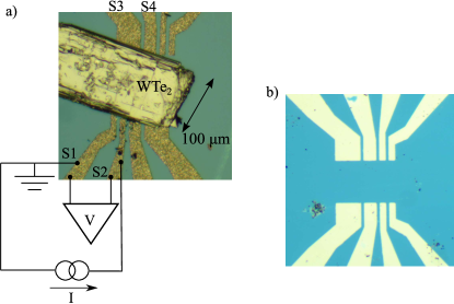
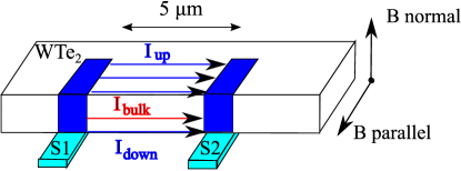
A sample sketch is presented in Fig. 1. Superconducting leads are formed by lift-off technique after thermal evaporation of 100 nm indium on the insulating SiO2 substrate, see Fig. 1 (b). A WTe2 single crystal ( dimensions) is placed on the indium leads pattern, and is weakly pressed by another Si/SiO2 substrate. The substrates are kept strictly parallel by external metallic frame to avoid sliding of the WTe2 crystal, which is verified in optical microscope. As a result, planar In-WTe2 junctions are formed at the bottom surface of the crystal WTe2, being separated by 5 m intervals, as depicted in Fig. 1.
The obtained In-WTe2-In SNS structures should be regarded as long diffusive ones: the value exceeds the mean free path wte2mobility in WTe2 1 m, so it should be compared kulik-long ; dubos with the coherence length of the diffusive SNS junction nm, where Fermi velocity is from ARPES data bruno , and meV is the indium superconducting gap indium . This estimation is even stronger for smaller , which can be expected ali-mag-res from the magnetoresistance behavior of our samples inwte ; ndwte .
Charge transport is investigated between two superconducting indium leads in a four-point technique. An example of electrical connections is presented in Fig. 1 (a): the S1 electrode is grounded; a current is fed through the S2; a voltage drop is measured between these S1 and S2 electrodes by independent wires. In this connection scheme, all the wire resistances are excluded, which is necessary for low-impedance In-WTe2-In junctions (below 0.5 Ohm normal resistance in the present experiment). The measurements are performed in standard He4 cryostat in the temperature range 1.4 K – 4.2 K. The indium leads are superconducting below the critical temperature indium .
III Experimental results
III.1 curves
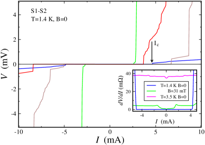
To obtain characteristics, we sweep the dc current and measure the voltage drop . Fig. 2 presents examples for different samples in zero magnetic field and at low temperature 1.4 K.
The curves in Fig. 2 clearly demonstrate Josephson effect in unprecedentedly long 5 m In-WTe2-In junctions: (i) by the four-point connection scheme we directly demonstrate zero resistance region at low currents (with m accuracy, see the inset); (ii) the non-zero resistance appears as sharp jumps at current values mA for different samples; (iii) curve can be switched to standard Ohmic behavior, if superconductivity is suppressed by temperature or magnetic field, as it is demonstrated in the inset to Fig. 2.
The obtained values differ within 10% in different coolings for a given sample. They are much smaller than the critical current for the indium leads, which can be estimated as mA for the leads’ dimensions and the known in-current maximum value A/cm2 for indium. There are also small jumps in the resistive state at intermediate currents mA for some samples, see Fig. 2.
III.2 curves under microwave irradiation
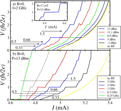
The main experimental finding is the observation of fractional a.c. Josephson effect, as it is depicted in Fig. 3. The sample is illuminated by microwave (rf) radiation through an open coaxial line. For the fixed frequency, see Fig. 3 (a), rising of the radiation power shifts to lower currents. Simultaneously, Shapiro steps appears, which are placed at , as it should be expected for typical SNS junctions with trivial periodicity in current-phase relationship .
In addition to the steps at integer , we observe half-integer ones, i.e., periodicity in a.c. Josephson effect. It usually appears due to interference effects rfpan ; rfli , for example, for the double-slit geometries in superconducting quantum interference devices (SQUID) bezryadin ; iran . The situation is even more complicated at high power: there are clear-visible steps, which obviously indicates a multivalued nonsinusoidal character of the current-phase relationship bezryadin ; iran .
Fig. 3 also demonstrates dependence of integer and fractional Shapiro steps on the microwave power (a), magnetic field (inset to (a)), and microwave frequency (b). The fractional steps are the weakest: they can be suppressed by lowest magnetic field, while the one is as robust as the integer Shapiro steps, see the inset to Fig. 3 (a). Also, while decreasing the frequency at constant power, steps disappear first, which is demonstrated in Fig. 3 (b). On the other hand, the integer step is the most stable: it appears at lowest power and frequency, see Fig. 3, and it is the strongest at highest ones. This robustness of the Shapiro step is just the opposite to the observed periodicity ( disappearance) in Al-Cd3As2-Al or Nb-Cd3As2-Nb junctions rfpan ; rfli .
III.3 Check of possible fabrication defects
First of all, we should experimentally exclude artificial reasons for the observed multivalued character of the current-phase relationship, particularly possible fabrication defects, like multiple indium shortings in the junction plane. The thickness of the indium film is chosen to be much smaller than the leads separation (100 nmm) to avoid parasite shorting of In leads. Moreover, we do not see Josephson current in 5 m long In-Cd3As2-In junctions, prepared in the same technique cdasJ , so the observed behavior is specific for WTe2.
The crucial arguments can be obtained from the maximum supercurrent behavior with temperature or magnetic field.
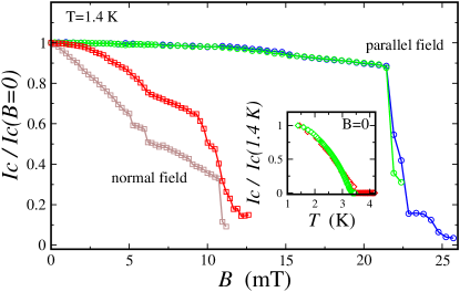
To analyze behavior, we use characteristics like ones presented in the right inset to Fig. 2: the dc current is additionally modulated by a low ac component (100 nA, 10 kHz), an ac part of () is detected by a lock-in amplifier. We have checked, that the lock-in signal is independent of the modulation frequency in the 6 kHz – 30 kHz range, which is defined by applied ac filters. To obtain values with high accuracy for given values, we sweep current ten times from zero (superconducting state) to above (resistive state), and then determine as the average value of jump positions in different sweeps. The results are presented in Fig. 4. All the experimental points are well reproducible, variation of in different sweeps is below the symbol size for data in Fig. 4.
(i) The experimental in the inset to Fig. 4 is inconsistent with indium shortings, because does not demonstrate strong decay in the high-temperature limit , which is expected kulik-long ; dubos for long diffusive SNS junctions. Instead, the experimental dependence is even slower than the linear function of in Fig. 4 (a). Similar behavior has been also demonstrated in long (1.5-2 m) graphene SNS junctions calado ; borzenets , where it has been attributed to topological edge state transport.
(ii) To our surprise, pattern crucially depends on the magnetic field orientation to the In-WTe2-In junction plane, see Fig. 4. If the magnetic field is perpendicular to the plane, strong suppression of is observed, as it can be expected for standard Josephson junctions due to the pair breaking effect cuevas . In contrast, is diminishing very slowly (within 10% until the critical field) for the parallel magnetic field, which indicates interference effects, like in non-symmetric double-slit SQUID geometries yakoby ; kowen . It indicates, that the effective SQUID area is perpendicular to the junction plane and, thus, it can not be formed by parasite In shortings: if several fabrication defects connected the leads on the SiO2 surface, they could form SQUID-like geometry in the junction plane only.
IV Discussion
Since we can exclude parasite shortings in the junction plane, we should connect the observed multivalued character of the current-phase relationship with non-trivial distribution yakoby ; kowen ; inwte ; rfpan of the Josephson current within the WTe2 crystal, i.e., with topological surface states armitage ; wang ; mazhar ; wang-miao .
The interference ( periodicity) can appear if both surface and bulk carriers transfer Josephson current in parallel, see Fig. 5, as it has been proposed for Cd3As2 Dirac semimetal rfpan ; rfli . This picture gives qualitatively reasonable results: (i) Parallel magnetic field induces a phase shift between surface and bulk channels for Josephson current, which leads to slow damping, as we observe in Fig. 4. If the magnetic field is perpendicular to the WTe2 crystal plane, both surface and bulk channels are in phase. (ii) Half-integer Shapiro steps appears in Fig. 3 due to interference between bulk and surface channels, similarly to Cd3As2 Dirac semimetal rfpan ; rfli .
However, the clear visible Shapiro steps at fractional indicates that the interference scheme for Josephson current is more complicated bezryadin ; iran for WTe2. This is the reason to consider also the surface states on the opposite sample surface, see Fig. 5, which are not independent in Weyl semimetal armitage . Due to the necessity of the surface state coupling, the contribution of this channel can only be seen at maximum microwave power and frequency in Fig. 3.
Another evidence on the Weyl specifics of the WTe2 surface states is the fact, that we do not observe periodicity in a.c. Josephson effect: the integer Shapiro step is the strongest one at highest power in Fig. 3, while the maximum power value covers the range of disappearance in Al-Cd3As2-Al and Nb-Cd3As2-Nb junctions rfpan ; rfli . In the latter case, periodicity is connected rfpan ; rfli with the helical nature of topological surface states in Dirac semimetals, while Weyl surface states inherit the chiral property of the Chern insulator edge states armitage .
Because of topological protection, Weyl surface states can efficiently transfer the Josephson current, which appears in slow decay in the inset to Fig. 4. This is another argument for the surface states, since the bulk supercurrent contribution should demonstrate strong exponential decay kulik-long ; dubos in the high-temperature limit for long diffusive SNS junctions.
V Conclusion
As a conclusion, we experimentally study electron transport between two superconducting indium leads, coupled to a single WTe2 crystal, which is a three-dimensional Weyl semimetal. We demonstrate Josephson current in long 5 m In-WTe2-In junctions, as confirmed by the observation of integer (1,2,3) and fractional (1/3, 1/2, 2/3) Shapiro steps under microwave irradiation. Demonstration of fractional a.c. Josephson effect indicates multivalued character of the current-phase relationship, which we connect with Weyl topological surface states contribution to Josephson current. In contrast to topological insulators and Dirac semimetals, we do not observe periodicity in a.c. Josephson effect for WTe2 at different frequencies and power, which might reflect chiral character of the Fermi arc surface states in Weyl semimetal.
Acknowledgements.
We wish to thank Yu.S. Barash, Ya. Fominov, V.T. Dolgopolov for fruitful discussions, and S.S Khasanov for X-ray sample characterization. We gratefully acknowledge financial support by the RFBR (project No. 16-02-00405) and RAS.References
- (1) M. Z. Hasan and C. L. Kane, Rev. Mod. Phys. 82, 3045 (2010).
- (2) X.-L. Qi and S.-C. Zhang, Rev. Mod. Phys. 83, 1057 (2011).
- (3) A. Bansil, H. Lin, and T. Das, Rev. Mod. Phys. 88, 021004 (2016).
- (4) C.-K. Chiu, J. C. Teo, A. P. Schnyder, and S. Ryu, Rev. Mod. Phys. 88, 035005 (2016).
- (5) As a recent review see N. P. Armitage, E. J. Mele, and A. Vishwanath, Rev. Mod. Phys. 90, 15001 (2018).
- (6) Ch. Wang, Y. Zhang, J. Huang, S. Nie, G. Liu, A. Liang, Yu. Zhang, B. Shen, J. Liu, C. Hu, Y. Ding, D. Liu, Y. Hu, S. He, L. Zhao, L. Yu, J. Hu, J. Wei, Z. Mao, Y. Shi, X. Jia, F. Zhang, S. Zhang, F. Yang, Z. Wang, Q. Peng, H. Weng, X. Dai, Z. Fang, Z. Xu, C. Chen, and X.J. Zhou, Phys. Rev. B 94, 241119(R) (2016).
- (7) Y. Wu, D. Mou, N.H. Jo, K. Sun, L. Huang, S.L. Bud’ko, P.C. Canfield, A. Kaminski, Phys. Rev. B 94, 121113(R) (2016).
- (8) Mazhar N. Ali, Jun Xiong, Steven Flynn, Jing Tao, Quinn D. Gibson, Leslie M. Schoop, Tian Liang, Neel Haldolaarachchige, Max Hirschberger, N. P. Ong and R. J. Cava Nature 514, 205 (2014). doi:10.1038/nature13763
- (9) Wang, Y. et al., Nat. Commun. 7, 13142 (2016). doi: 10.1038/ncomms13142
- (10) Sean Hart, Hechen Ren, Timo Wagner, Philipp Leubner, Mathias Mühlbauer, Christoph Brüne, Hartmut Buhmann, Laurens W. Molenkamp & Amir Yacoby, Nature Physics 10, 638–643 (2014), doi:10.1038/nphys3036
- (11) Vlad S. Pribiag, Arjan J. A. Beukman, Fanming Qu, Maja C. Cassidy, Christophe Charpentier, Werner Wegscheider & Leo P. Kouwenhoven, Nature Nanotechnology 10, 593 (2015)
- (12) O. O. Shvetsov, A. Kononov, A. V. Timonina, N. N. Kolesnikov, E. V. Deviatov, JETP Letters, 107, 774–779 (2018) https://doi.org/10.1134/S0021364018120020
- (13) V. E. Calado, S. Goswami, G. Nanda, M. Diez, A. R. Akhmerov, K. Watanabe, T. Taniguchi, T. M. Klapwijk & L. M. K. Vandersypen, Nature Nanotechnology 10, 761–764 (2015). doi:10.1038/nnano.2015.156
- (14) I.V. Borzenets, F. Amet, C.T. Ke, A.W. Draelos, M.T. Wei, A. Seredinski, K. Watanabe, T. Taniguchi, Y. Bomze, M. Yamamoto, S. Tarucha, and G. Finkelstein, Phys. Rev. Lett. 117, 237002 (2016), http://dx.doi.org/10.1103/PhysRevLett.117.237002
- (15) W. Yu, W. Pan, D.L. Medlin, M. A. Rodriguez, S.R. Lee, Z. Bao, F. Zhang, Phys. Rev. Lett. 120, 177704 (2018). doi:10.1103/PhysRevLett.120.177704
- (16) Cai-Zhen Li, Chuan Li, Li-Xian Wang, Shuo Wang, Zhi-Min Liao, Alexander Brinkman, Da-Peng Yu, Physical Review B 97, 115446 (2018) DOI: 10.1103/PhysRevB.97.115446
- (17) E. B. Borisenko, V. A. Berezin, N. N. Kolesnikov, V. K. Gartman, D. V. Matveev, O. F. Shakhlevich, Physics of the Solid State, 59, 1310, (2017).
- (18) A. Sidorov, A.E. Petrova, A.N. Pinyagin, N.N. Kolesnikov, S.S. Khasanov, S.M. Stishov, JETP, 122, 1047, (2016).
- (19) A. Kononov, O. O. Shvetsov, S. V. Egorov, A. V. Timonina, N. N. Kolesnikov and E. V. Deviatov EPL, 122, 27004 (2018) doi: 10.1209/0295-5075/122/27004
- (20) H.Y. Lv, W.J. Lu1, D.F. Shao, Y. Liu, S.G. Tan and Y.P. Sun, EPL 110 37004 (2015).
- (21) I. O. Kulik, Sov. Phys. JETP 30, 944 (1970).
- (22) P. Dubos, H. Courtois, B. Pannetier, F. K. Wilhelm, A. D. Zaikin, and G. Schön Phys. Rev. B 63, 064502 (2001)
- (23) F.Y. Bruno, A. Tamai Q.S. Wu, I. Cucchi, C. Barreteau, A. de la Torre, S. McKeown Walker, S. Riccò, Z. Wang, T.K. Kim, M. Hoesch, M. Shi, N.C. Plumb, E. Giannini, A.A. Soluyanov, and F. Baumberger, Phys. Rev. B 94, 121112(R) (2016).
- (24) A. M. Toxen Phys. Rev. 123, 442 (1961).
- (25) Mazhar N. Ali, Leslie Schoop, Jun Xiong, Steven Flynn, Quinn Gibson, Max Hirschberger, N. P. Ong and R. J. Cava, EPL, 110, 67002 (2015).
- (26) P. Scharnhorst Phys. Rev. B 1, 4295 (1970).
- (27) R. C. Dinsmore III, Myung-Ho Bae, and A. Bezryadin, Appl. Phys. Lett. 93, 192505 (2008); https://doi.org/10.1063/1.3012360
- (28) A Valizadeh, M R Kolahchi and J P Straley, Journal of Nonlinear Mathematical Physics, 15, 407–416 (2008).
- (29) Will be published elsewhere
- (30) J. C. Cuevas and F. S. Bergeret, Phys. Rev. Lett. 99, 217002 (2007).
- (31) R. Vijay, E. M. Levenson-Falk, D. H. Slichter, and I. Siddiqi, Appl. Phys. Lett. 96, 223112 (2010); doi: 10.1063/1.3443716