A CMOS dynamic random access architecture for radio-frequency readout of quantum devices.
Abstract
Quantum computing technology is maturing at a relentless pace, yet individual quantum bits are wired one by one. As quantum processors become more complex, they require efficient interfaces to deliver signals for control and readout while keeping the number of inputs manageable. Digital electronics offers solutions to the scaling challenge by leveraging established industrial infrastructure and applying it to integrate silicon-based quantum devices with conventional CMOS circuits. Here, we combine both technologies at milikelvin temperatures and demonstrate the building blocks of a dynamic random access architecture for efficient readout of complex quantum circuits. Our circuit is divided into cells, each containing a CMOS quantum dot (QD) and a field-effect transistor that enables selective readout of the QD, as well as charge storage on the QD gate similar to 1T-1C DRAM technology. We show dynamic readout of two cells by interfacing them with a single radio-frequency resonator. Our results demonstrate a path to reducing the number of input lines per qubit and enable addressing of large-scale device arrays.
pacs:
Valid PACS appear hereQuantum computers promise to solve problems which seem intractable using conventional computers Montanaro (2016). Several different physical implementations of a quantum computer are being developed Ladd et al. (2010) and state-of-the-art processors are approaching the level of 50 to 100 quantum bits (or qubits) where quantum computers are expected to demonstrate capabilities beyond conventional computers for specific tasks Neill et al. (2018).
For most physical realizations, quantum processors require cryogenic temperatures to operate, precise low-noise control signals van Dijk et al. (2018) to manipulate the information and highly sensitive readout techniques to extract the results; all without disturbing the fragile quantum states. In current solid-state quantum processors, signals are generated using general-purpose instruments at room temperature and delivered to the quantum processor at low temperatures. The physical qubits across all platforms are controlled directly with at least one control line per qubit. However, as the size of quantum processors continues to increase, the one-qubit-one-input approach is recognized to be unsustainable Franke et al. (2018), especially if we consider that a large-scale fault-tolerant quantum computer might ultimately require qubits to solve the most computationally demanding algorithms Fowler et al. (2012). Efficiently delivering control and readout signals to increasingly more complex quantum circuits while reducing the number of inputs per qubit is one of the major challenges towards a fully-fledged large-scale universal quantum computer.
Digital electronics may offer some opportunities to overcome this difficulty. Some of the challenges that large-scale quantum computing faces resemble those that conventional computing has already solved. A perfect example is controlling billions of transistors with just a few thousands of input-output connections. Moreover, integrated digital electronics allows signal generation, data flow management, low-level feedback and high-level operations locally. Therefore, to relax wiring requirements and reduce the latency of solid-state quantum computers, integration of digital electronics with quantum devices at cryogenic temperatures could be a promising strategy Reilly (2015); Hornibrook et al. (2015). Nevertheless, to apply this approach, understanding the behaviour of digital circuits at cryogenic temperatures is paramount.
Digital information processing devices are typically manufactured using silicon as the base material. Coincidentally, electron spins in silicon are amongst the most promising candidates for large-scale quantum computing Kane et al. (1998); Loss and DiVincenzo (1998) due to their small footprint (sub nm dimensions) and very long coherence times, particularly in isotopically purified silicon (28Si) Veldhorst et al. (2015); Muhonen et al. (2014). Silicon-based spin qubits benefit from a variety of qubit designs and different coupling strategies Veldhorst et al. (2015); Eng et al. (2015); Urdampilleta et al. (2015); Zajac et al. (2016); Mi et al. (2017); Maurand et al. (2016); House et al. (2015); Shi et al. (2012); Harvey-Collard et al. (2018); Kawakami et al. (2014); Watson et al. (2018); Zajac et al. (2017); Weber et al. (2014) and can be read out dispersively using Pauli spin-blockade Betz et al. (2015); West et al. (2018); Pakkiam et al. (2018). To date, operation of one-dimensional arrays has been shown Zajac et al. (2016), high-fidelity single qubit gates Veldhorst et al. (2014); Takeda et al. (2016); Yoneda et al. (2018); Huang et al. (2018) and two qubit gates Veldhorst et al. (2015); Zajac et al. (2017) have been achieved and a programmable two-qubit silicon-based processor has been demonstrated Watson et al. (2018).
Recently, it was shown that CMOS transistors can be used as the basis for spin qubits Maurand et al. (2016); Crippa et al. (2018). Several other silicon-based quantum devices could, in principle, be realised in a manner compatible with industrial CMOS processes, with the potential of large-scale, high-yield fabrication. It seems then natural to explore the direct integration of silicon quantum devices and conventional CMOS digital technology to tackle the challenges in addressing, controlling and reading multi-qubit circuits. Blueprints of such all-silicon systems integrating quantum and classical components have emerged Veldhorst et al. (2017); Vandersypen et al. (2017); Li et al. (2018) as well as first basic demonstrations of direct integration Schaal et al. (2018).
Here, we present a CMOS dynamic random access architecture for control and readout of multiple quantum devices. Our design is inspired by the square arrays found in dynamic random access memory (1T-1C DRAM) and allows on-demand routing of static and radio-frequency (rf) signals to individual devices. The architecture is composed of individual cells each containing a control field-effect transistor (“control FET”) and a quantum dot (QD) device. In our experiments, the QDs are themselves formed in the channel of a nanowire FET, integrated on the same chip as the control FETs and fabricated using the same CMOS processes. When not addressed, each cell can be used as a node to store charge on the QD device gate that allows trapping single-electrons in the QD device with a time constant approaching s. In this Article, we demonstrate random access and readout of two individual cells at cryogenic temperatures. For readout, we use capacitive gate-based radio-frequency reflectometry that turns the gate defining the quantum dot into a sensor by coupling it to a lumped-element resonant circuit Colless et al. (2013); Gonzalez-Zalba et al. (2015); Ahmed et al. (2018). We characterize the bandwidth of the architecture in terms of a resonant frequency overlap of MHz, and find optimal operation voltage levels for the digital transistor. Moreover, we show dynamic readout of the cells and obtain charge stability maps sequentially. Finally, we propose an architecture for addressing large-scale device arrays with a quadratic reduction in the number of inputs.
I Circuit characterization
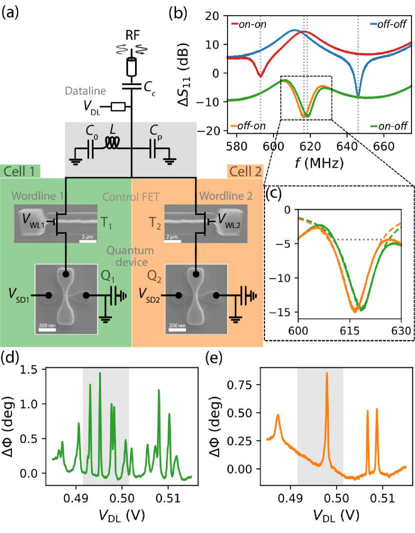
We show the sequential access circuit in Fig. 1(a). It consists of two CMOS single-electron memory cells Schaal et al. (2018) (cell 1(2) in green(orange)) connected to a single bias line and a lumped-element radio-frequency resonator for readout (resonator components are highlighted in grey). Each memory cell is made from two transistors which we refer to as Qi and Ti. Qi is a 60-nm-wide silicon nanowire transistor with a short channel length ( and nm for cell 1 and 2 respectively). Such devices are routinely used to trap single-electrons in quantum dots that form at the top most corners of the nanowire channel when operated in the sub-threshold regime at cryogenic temperatures Voisin et al. (2014); Gonzalez-Zalba et al. (2016). Transistor Ti is a wider device with a channel width of m and gate length of nm and nm for cell 1 and 2 respectively which we refer to as the control FET. The four transistors are manufactured using fully-depleted silicon-on-insulator (FD-SOI) technology following standard CMOS processes. They are located on the same chip and are connected via bond wires (see Methods for details of the fabrication).
We label the primary inputs of the circuit as data and word lines in analogy with memory chips. Each cell has one word line which connects to the gate of the control FET Ti allowing control over the channel resistance. The data line is shared among the two cells and allows control over the gate voltage on Qi conditional on the state of Ti. Additionally, a voltage applied to the silicon substrate, , acts as a back-gate. Switching Ti to the on state while keeping all the remaining Tj off allows for individual addressing of a single quantum device Qi. Multiple devices can be addressed sequentially by timing the voltages on Ti accordingly, as we demonstrate further below.
To read the quantum state of the devices sequentially, we connect a lumped-element resonator in parallel with the memory cells and use radio-frequency reflectometry to probe the resonant state of the combined circuit Schaal et al. (2018). The natural frequency of the resonator is given by where is the total capacitance of the system that includes, in particular, the state-dependent quantum or tunneling capacitance of any quantum device which is connected to the LC circuit Mizuta et al. (2017) via the control FETs. We drive the resonator with a small ( dBm) radio-frequency signal at frequency that we coupled into the data line via a bias tee. The whole circuit is operated in a dilution refrigerator with a base temperature of mK.
Next, we show the frequency dependence of the circuit’s reflection coefficient in Fig. 1(b) for the four possible states of the two control FETs. A dip in the reflection coefficient occurs when we drive the resonator at its natural frequency of oscillation, which shifts towards lower frequency for each Ti in the on state due to the additional circuit capacitance introduced by the enabled cell (by approximately MHz, see Supplementary Table S1 for resonance parameters). Most importantly, we observe a large spectral overlap of MHz with dB bandwidth in the enlarged view in Fig. 1(c) when addressing one cell at a time. Spectral overlap is paramount to dynamical multi-qubit readout as it means that both cells can be read using the same input frequency, while the degree of overlap determines the bandwidth of the architecture. In addition to the resonance frequency shift, we observe a reduction in the loaded quality factor from a value of 96, when both T1 or T2 are in the off state, to a value of 40, when either T1 or T2 are in the on state. An on-state of 40 is comparable to previous experiments with Schaal et al. (2018) and without Gonzalez-Zalba et al. (2015) control circuit.
Based on the spectra shown in Fig. 1(c), we select a carrier frequency MHz to probe the state of the quantum devices. When using radio-frequency reflectometry, changes in the complex impedance of the circuit are probed by driving the circuit close to resonance while monitoring the phase and magnitude of the reflected signal (see Methods for details of the circuit). Changes in the capacitance of the quantum device , attributed to tunneling of single electrons, are detected through changes in the reflected phase Ahmed et al. (2018). In Fig. 1(d-e), we observe phase shift peaks as we change that corresponds to regions of charge instability in Qi. At these voltages, single electrons cyclically tunnel between the QDs in the channel and the source or drain electron reservoirs in Qi. For each measurement only one Ti is set to the on state while the other is off. Below we perform further measurement focusing on a particular region of this stability diagram (highlighted in Fig. 1(d-e)) for both quantum devices.
II Digital transistor operation parameters
In this section, we focus on the digital operation of the control transistors with the aim to find the optimal voltage levels. For a dynamical random-access readout scheme, Ti should fulfill several requirements: In the on state, Ti should be sufficiently conductive to allow high-sensitivity gate-based readout of the selected quantum device. In the off state, Ti should be sufficiently resistive to block the rf signal to deselected cells and to retain the charge on Qi’s gate for the duration operations are being performed in other cells.
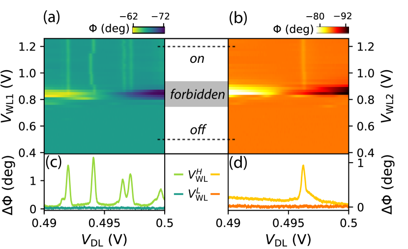
As a first step towards dynamically operating the circuit, we identify suitable on and off state voltages for the control FET gate (i.e. the high, , and low, , signal levels). In Fig. 2(a-b), we show the phase of the reflected signal from the resonator as a function of and in the areas highlighted in Fig. 1(d-e). We can identify three regions: The on region for V, where we observe single electron tunneling, the off region for V, where we observe no transitions and finally, for 0.7 V V the forbidden region. In the latter, Ti is in the saturation regime, where, due to the voltage-dependence gate capacitance of the control FET, the phase varies largely Rossi et al. (2017). This region should be avoided when assigning voltage levels. To highlight the different response of the resonator in the digital on and off states, we show the phase change as a function of for cell 1 and 2 in Fig. 2(c-d), respectively, at V (as indicated by the dashed black lines in Fig. 2(a-b)).
We note the close similarity between the operation voltage levels of both Ti for addressing the quantum devices Qi at millikelvin temperature. In a scaled up architecture, with increasing circuit complexity, reproducible electrical characteristics between cells will be essential.
III Dynamic Operation
III.1 Charge retention time
Random access of a single cell can be achieved by switching the selected Ti on while all other Tj are off. Since the data line voltage is shared among the cells, the gate voltage on all deselected Qj floats and decays over time while addressing cell . Floating gate charge storage, which is also found in modern dynamic random access memory (DRAM) chips, is an important feature of dynamic readout and its associated charge retention time sets the maximum time to perform operations on other cells before the information is lost.
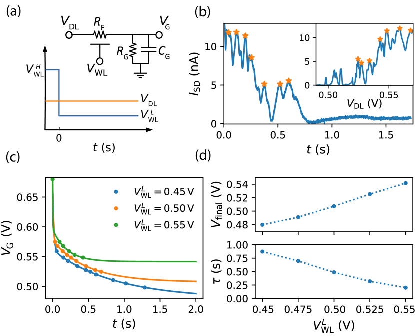
In this section, we characterize the discharge of one cell in order to determine an appropriate voltage refresh rate. We consider the equivalent circuit model of the memory cell as shown in Fig. 3(a) with a -dependent channel resistance of the control FET and a gate resistance of the quantum device combined with a capacitance , realizing charge storage on the quantum device gate. has a contribution from the FET, the quantum device gate and the parasitic capacitance of the inter-connection. The latter dominates in this experiment (see Supplementary Table S1 and Note). In the on state, the voltage on the gate capacitor is charged to , while in the off state decays over time as
| (1) |
Here is the circuit time constant and is the equilibrium voltage at the gate of the quantum device at . Since and depend on , and thus on the operation voltage level , we proceed by investigating their functional dependence further in order to find the optimal voltage operation point to maximize the charge retention time.
We monitor the discharge of the cell in a pulsed experiment by measuring the source-drain current through the quantum device over time. As shown in Fig. 3(a), we keep constant while switches from the high level () to a low level () at . We set the pulse amplitude to 0.5 V and vary the pulse offset ensuring that the transistor remains on in the high part of the pulse. We show an example discharge measurement for V in Fig. 3(b), where several single electron transitions (indicated by stars) can bee observed in over time. After s the current settles to a value determined by . We compare the discharge data with a measurement of the same single electron transitions of the device as a function of in quasi-static conditions as shown in the inset of Fig. 3(b). By matching peaks in the decay over time to peaks as a function of we reproduce the dynamics of the voltage on the quantum device gate as shown in Fig. 3(c) for multiple values of . At , we observe an initial fast decay, possibly due to cross-talk, followed by a slow decay characterized by Eq. 1. We fit a double exponential to capture the fast and slow dynamics (see Supplementary Note) and extract and from the slow decay which we show in Fig. 3(d) as a function of . We observe that as increases ( decreases) becomes larger due to the voltage divider characteristic of the cell (see panel (a)). In the case of , we observe a reduction from s to s. Both trends are captured in our model. We note that the time constant could be increased further for a larger capacitance .
While initially it may seem beneficial to select a low level to maximize , the retention or refresh time is determined by the maximum tolerable gate voltage drop of the cell, , which has to be accessed given a specific qubit implementation. Using our model and defining the voltage drop ratio and the resistance ratio , we find that the retention time is given by which is a monotonically increasing function of . Hence, is maximized by operating at large while remaining in the off regime.
In this analysis, it is important to note that we keep constant which is approximately what will happen when addressing multiple quantum devices with similar operating voltages. Such operation is a particular feature of our proposal and differs from the 1T-1C DRAM read protocol where is typically set to half the maximum voltage stored in the capacitor. Such voltage level maximizes the readout signal and the retention time of both the uncharged and charged memory state of the capacitor David Tawei Wang (2005). In our proposal, we operate exclusively at the charged state of Qi where retention time is maximized by selecting a less resistive FET, i.e. as large as possible while remaining in the off state. For sequential readout, as demonstrated further below, we select V to enhance the retention time in the off state while preserving good noise margins.
III.2 Dynamic power dissipation
Having extracted the digital voltage levels for the control FETs, we can estimate the dynamic power dissipation of the architecture. This parameter is important when operating at the base temperature of a dilution refrigerator where limited cooling power, typically 400 W, is available. The dynamic power when switching Ti is , where , is the additional capacitance introduced by switching Ti to the on state and is the switching frequency. The maximum is given by the bandwidth of the architecture and by the gate area of the FET plus the parasitic capacitance of the interconnect between Ti with Qi. Given our selection of V, the bandwidth 13 MHz and fF (see Supplementary Table S1), we estimate 0.4 W/cell which will allow operating 1,000 cells simultaneously. The power dissipation can be reduced by pushing the voltage levels closer to the forbidden region V, thus reducing the noise level margins, and by minimizing by optimizing the circuit layout. The minimum will be the dominated by the geometric capacitance of Ti of 8 fF. At the same frequency of operation the dissipation will be W/cell extending the number of cells that can be operated at the same time to 20,000. When reducing the circuit capacitance the noise associated with charging the cell via the control FET resistance should be considered . In this experiment we estimate the noise at V (15 mK base temperature).
III.3 Sequential readout
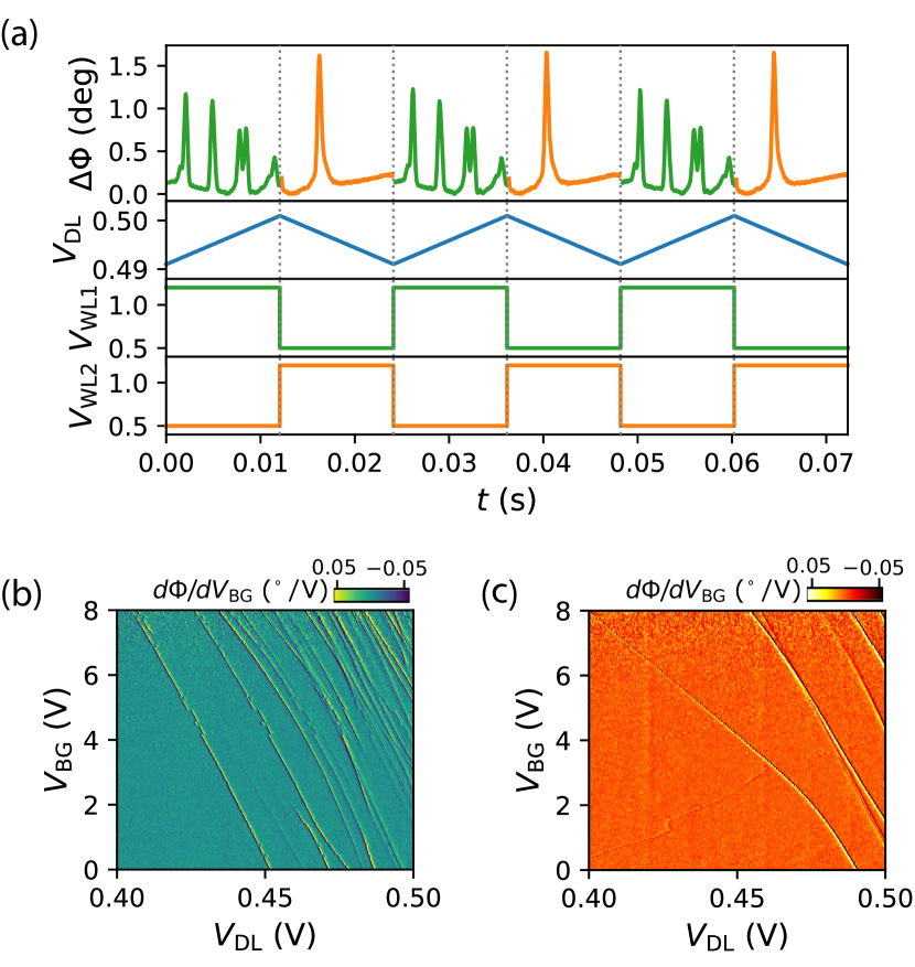
We now turn to demonstrate sequential dynamic readout of quantum devices in two memory cells. We show the pulsing scheme to dynamically read both memory cells in Fig. 4(a).
In the first half of the cycle, from 0 to 12 ms, we set T1 and T2 to the digital on and off states respectively. Simultaneously, we apply an analogue signal to the common data line (blue trace) that ramps up the gate voltage on the data line (now connected to Q1). We read the signal dispersively using gate-based readout and detect peaks in the phase due to single-electron transitions between a QD and a reservoir in Q1.
In the second half of the cycle, from 12 to 24 ms, we invert the digital voltages on T1 and T2 such that we can now detect the transitions in Q2 as we ramp down the analogue signal on the data line. The QD-to-reservoir transitions in the phase response are identical to those measured in a static experiment shown in Fig. 1(d-e). The rf modulation frequency and amplitude is kept constant throughout the measurement. There is a phase offset between the signal detected from Q1 and Q2 due to a small difference in reflection coefficient between cells (see Fig. 1(c)). We therefore show the phase difference in Fig. 4(a) (see Supplementary Figure S2).
Using this interleaved pulsing scheme for sweeping combined with additional stepping of after each cycle, we obtain the charge stability map of both Q1 and Q2 sequentially as shown in Fig. 4(b-c). The transitions observed in the measurement suggest formation of multiple QDs in both cells (see Supplementary Figure S1 for additional scans), i.e. corner dots Voisin et al. (2014); Betz et al. (2014). Due to filtering of the lines delivering the control FET signals and data line signal , was limited to kHz in this experiment (see Supplementary Figure S2).
IV Discussion: Scaling up the architecture
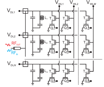
In this Article, we have presented a CMOS dynamic-random-access architecture for radio-frequency readout of quantum dot devices at millikelvin temperature. In particular, we performed sequential dispersive readout of individual quantum devices in a two-cell layout. In this section, we describe how a larger () array of randomly addressable single-electron memory cells could be constructed, making use of the sequential gated readout we demonstrate above, combined with frequency multiplexing. As shown in Fig. 5, the two dimensional array is distributed in rows () and columns (). A specific qubit in row and column , Qij, can be addressed by a word line , that controls the voltage on the gate of transistor Tij, and by a data line voltage , that controls the gate potential on the qubit. Additionally, each row is connected to a different resonator for readout. Distinct resonant frequencies are achieved using different values for the inductance of each resonator . Note that the inductors have a low high-frequency impedance to ground in parallel with a parasitic capacitor. Each resonator can be probed simultaneously using frequency multiplexing techniques Hornibrook et al. (2014) such that the whole array only requires a sole high-frequency line for readout. The array can be operated dynamically in a random access manner. When a specific word line is activated qubits Q can be read simultaneously for all or their gate voltages are refreshed using the specific data line voltages . Each qubit may be fabricated such that it is in close proximity to other qubits to perform two-qubit operations Zajac et al. (2018); Watson et al. (2018). This possibility is indicated by the circular connection at the source of each quantum device. The array particularly suits one dimensional chains of interacting quantum devices such as they are distributed along the rows of the array Betz et al. (2016); Zajac et al. (2016); Jones et al. (2018).
For further optimization of the architecture a more detailed understanding of each circuit component at low temperature is necessary, including cross-talk mitigation and a circuit equivalent model of both the control FETs and the quantum devices at the desired operation bias and frequency. Such models could be used in combination with ECAD mixed-circuit design tools to produce an integrated circuit version of the 2D array. Moreover, we note when applying this proposed architecture to particular qubit implementations, where small voltage drifts may induce undesired effects such as unwanted decoherence, further optimization could be necessary to find an optimal trade off between voltage noise, retention time and power dissipation depending on the cell’s capacitance. Finally, we note that the signal-to-noise of gate-based readout – limited by the quality factor of the resonant circuit – could be improved by using superconducting spiral inductors Ahmed et al. (2018). There is a potential for such inductors to be made CMOS compatible using TiN allowing on-chip integration. The footprint of such inductors can be reduced when operating at higher frequencies which could ultimately enable an integrated solution for sensitive readout of large-density qubit arrays.
Methods
Fabrication details
All CMOS transistors used in this study were fabricated on SOI substrates with a -nm-thick buried oxide and -nm-thick silicon layer. The silicon layer is patterned to create the channel by means of optical lithography, followed by a resist trimming process. All transistors share the same gate stack consisting of nm HfSiON capped by nm TiN and nm polycrystalline silicon leading to a total equivalent oxide thickness of nm. The Si thickness under the HfSiON/TiN gate is nm. After gate etching a SiN layer ( nm) was deposited and etched to form a first spacer on the sidewalls of the gate. 18-nm-thick Si raised source and drain contacts were selectively grown before the source/drain extension implantation and activation annealing. A second spacer was formed followed by source/drain implantations, activation spike anneal and salicidation (NiPtSi). The wide channel control FETs and nanowire quantum devices are connected via on-chip aluminium bond wires.
Measurement setup
Measurements were performed at base temperature of a dilution refrigerator ( mK). Low frequency signals (, , ) were delivered through filtered cryogenic loom while a radio-frequency signal for gate-based readout was delivered through an attenuated and filtered coaxial line which connects to a on-PCB bias tee combining the rf modulation with . The resonator is formed from a nH inductor and the sample’s parasitic capacitance to ground in parallel with the device. The inductor consists of a surface mount wirewound ceramic core (EPCOS B82498B series) and the PCB is made from mm thick RO4003C with immersion silver finish. The reflected rf signal is amplified at K (LNF-LNC0.6_2A) and room temperature followed by quadrature demodulation (Polyphase Microwave AD0540B) from which the amplitude and phase of the reflected signal is obtained (homodyne detection).
Acknowledgements.
We would like to thank Sebastian Pauka for helpful discussions. This research has received funding from the European Union’s Horizon 2020 research and innovation programme under grant agreement No 688539 (http://mos-quito.eu) and Seventh Framework Programme (FP7/2007-2013) through Grant Agreement No. 318397 (http://www.tolop.eu.); as well as by the Engineering and Physical Sciences Research Council (EPSRC) through the Centre for Doctoral Training in Delivering Quantum Technologies (EP/L015242/1) and UNDEDD (EP/K025945/1). M.F.G.Z. and A.R. acknowledge support from the Winton Programme for the Physics of Sustainability and Hughes Hall, University of Cambridge.Author contributions
S.S. and M.F.G.-Z. devised the experiment. S.S., A.R. and M.F.G.-Z. performed the experiments; S.B. fabricated the sample; S.S. did the analysis and prepared the manuscript with contributions from A.R., J.J.L.M. and M.F.G.-Z.
Data availability
The data that support the findings of this study are available from the corresponding author upon reasonable request.
References
- Montanaro (2016) Ashley Montanaro, “Quantum algorithms: an overview,” npj Quantum Information 2, 15023 (2016).
- Ladd et al. (2010) T D Ladd, F Jelezko, R Laflamme, Y Nakamura, C Monroe, and J L O’Brien, “Quantum computers.” Nature 464, 45–53 (2010).
- Neill et al. (2018) C. Neill, P. Roushan, K. Kechedzhi, S. Boixo, S. V. Isakov, V. Smelyanskiy, A. Megrant, B. Chiaro, A. Dunsworth, K. Arya, R. Barends, B. Burkett, Y. Chen, Z. Chen, A. Fowler, B. Foxen, M. Giustina, R. Graff, E. Jeffrey, T. Huang, J. Kelly, P. Klimov, E. Lucero, J. Mutus, M. Neeley, C. Quintana, D. Sank, A. Vainsencher, J. Wenner, T. C. White, H. Neven, and J. M. Martinis, “A blueprint for demonstrating quantum supremacy with superconducting qubits,” Science 360, 195–199 (2018).
- van Dijk et al. (2018) Jeroen P. G. van Dijk, Erika Kawakami, Raymond N. Schouten, Menno Veldhorst, Lieven M. K. Vandersypen, Masoud Babaie, Edoardo Charbon, and Fabio Sebastiano, “The impact of classical control electronics on qubit fidelity,” arXiv preprint 1803.06176 (2018).
- Franke et al. (2018) David P. Franke, James S. Clarke, Lieven M. K. Vandersypen, and Menno Veldhorst, “Rent’s rule and extensibility in quantum computing,” arXiv preprint 1806.02145 (2018).
- Fowler et al. (2012) Austin G. Fowler, Matteo Mariantoni, John M. Martinis, and Andrew N. Cleland, “Surface codes: Towards practical large-scale quantum computation,” Physical Review A 86, 032324 (2012).
- Reilly (2015) David J Reilly, “Engineering the quantum-classical interface of solid-state qubits,” npj Quantum Information 1, 15011 (2015).
- Hornibrook et al. (2015) J. M. Hornibrook, J. I. Colless, I. D. Conway Lamb, S. J. Pauka, H. Lu, A. C. Gossard, J. D. Watson, G. C. Gardner, S. Fallahi, M. J. Manfra, and D. J. Reilly, “Cryogenic Control Architecture for Large-Scale Quantum Computing,” Physical Review Applied 3, 024010 (2015).
- Kane et al. (1998) B. E. Kane, G. R. Facer, A. S. Dzurak, N. E. Lumpkin, R. G. Clark, L. N. Pfeiffer, and K. W. West, “Quantized conductance in quantum wires with gate-controlled width and electron density,” Applied Physics Letters 72, 3506–3508 (1998).
- Loss and DiVincenzo (1998) D Loss and D P DiVincenzo, “Quantum computation with quantum dots,” Physical Review A 57, 120–126 (1998).
- Veldhorst et al. (2015) M Veldhorst, C H Yang, J C C Hwang, W Huang, J P Dehollain, J T Muhonen, S Simmons, A Laucht, F E Hudson, K M Itoh, A Morello, and A S Dzurak, “A Two Qubit Logic Gate in Silicon,” Nature 526, 410–414 (2015).
- Muhonen et al. (2014) Juha T Muhonen, Juan P Dehollain, Arne Laucht, Fay E Hudson, Rachpon Kalra, Takeharu Sekiguchi, Kohei M Itoh, David N Jamieson, Jeffrey C. McCallum, Andrew S Dzurak, and Andrea Morello, “Storing quantum information for 30 seconds in a nanoelectronic device,” Nature Nanotechnology 9, 986–991 (2014).
- Eng et al. (2015) K. Eng, T. D. Ladd, A. Smith, M. G. Borselli, A. A. Kiselev, B. H. Fong, K. S. Holabird, T. M. Hazard, B. Huang, P. W. Deelman, I. Milosavljevic, A. E. Schmitz, R. S. Ross, M. F. Gyure, and A. T. Hunter, “Isotopically enhanced triple-quantum-dot qubit,” Science Adv. 1, e1500214 (2015).
- Urdampilleta et al. (2015) Matias Urdampilleta, Anasua Chatterjee, Cheuk Chi Lo, Takashi Kobayashi, John Mansir, Sylvain Barraud, Andreas C. Betz, Sven Rogge, M. Fernando Gonzalez-Zalba, and John J. L. Morton, “Charge Dynamics and Spin Blockade in a Hybrid Double Quantum Dot in Silicon,” Physical Review X 5, 031024 (2015).
- Zajac et al. (2016) D. M. Zajac, T. M. Hazard, X. Mi, E. Nielsen, and J. R. Petta, “Scalable Gate Architecture for a One-Dimensional Array of Semiconductor Spin Qubits,” Physical Review Applied 6, 054013 (2016).
- Mi et al. (2017) X Mi, J V Cady, D M Zajac, P W Deelman, and J R Petta, “Strong coupling of a single electron in silicon to a microwave photon,” Science 355, 156–158 (2017).
- Maurand et al. (2016) R Maurand, X Jehl, D. Kotekar-Patil, A Corna, H Bohuslavskyi, R. Laviéville, L Hutin, S Barraud, M Vinet, M Sanquer, and S. De Franceschi, “A CMOS silicon spin qubit,” Nature Communications 7, 13575 (2016).
- House et al. (2015) M G House, T Kobayashi, B Weber, S J Hile, T F Watson, J van der Heijden, S Rogge, and M Y Simmons, “Radio frequency measurements of tunnel couplings and singlet-triplet spin states in Si:P quantum dots.” Nature communications 6, 8848 (2015).
- Shi et al. (2012) Zhan Shi, C. B. Simmons, J. R. Prance, John King Gamble, Teck Seng Koh, Yun-Pil Shim, Xuedong Hu, D. E. Savage, M. G. Lagally, M. A. Eriksson, Mark Friesen, and S. N. Coppersmith, “Fast Hybrid Silicon Double-Quantum-Dot Qubit,” Physical Review Letters 108, 140503 (2012).
- Harvey-Collard et al. (2018) Patrick Harvey-Collard, Benjamin D’Anjou, Martin Rudolph, N. Tobias Jacobson, Jason Dominguez, Gregory A. Ten Eyck, Joel R. Wendt, Tammy Pluym, Michael P. Lilly, William A. Coish, Michel Pioro-Ladrière, and Malcolm S. Carroll, “High-Fidelity Single-Shot Readout for a Spin Qubit via an Enhanced Latching Mechanism,” Physical Review X 8, 021046 (2018).
- Kawakami et al. (2014) E Kawakami, P Scarlino, Daniel R. Ward, F R Braakman, D. E. Savage, M. G. Lagally, Mark Friesen, Susan N. Coppersmith, Mark A. Eriksson, and L M K Vandersypen, “Electrical control of a long-lived spin qubit in a Si/SiGe quantum dot.” Nat. Nano. 9, 666 (2014).
- Watson et al. (2018) T. F. Watson, S. G. J. Philips, E. Kawakami, D. R. Ward, P. Scarlino, M. Veldhorst, D. E. Savage, M. G. Lagally, Mark Friesen, S. N. Coppersmith, M. A. Eriksson, and L. M. K. Vandersypen, “A programmable two-qubit quantum processor in silicon,” Nature 555, 633–637 (2018).
- Zajac et al. (2017) D. M. Zajac, A. J. Sigillito, M. Russ, F. Borjans, J. M. Taylor, G. Burkard, and J. R. Petta, “Resonantly driven CNOT gate for electron spins,” Science 5965, eaao5965 (2017).
- Weber et al. (2014) Bent Weber, Y. H.Matthias Tan, Suddhasatta Mahapatra, Thomas F. Watson, Hoon Ryu, Rajib Rahman, Lloyd C.L. Hollenberg, Gerhard Klimeck, and Michelle Y. Simmons, “Spin blockade and exchange in Coulomb-confined silicon double quantum dots,” Nature Nanotechnology 9, 430–435 (2014).
- Betz et al. (2015) A. C. Betz, R. Wacquez, M. Vinet, X. Jehl, A. L. Saraiva, M. Sanquer, A. J. Ferguson, and M. F. Gonzalez-Zalba, “Dispersively Detected Pauli Spin-Blockade in a Silicon Nanowire Field-Effect Transistor,” Nano Letters 15, 4622–4627 (2015).
- West et al. (2018) A. West, B. Hensen, A. Jouan, T. Tanttu, C. H. Yang, A. Rossi, M. F. Gonzalez-Zalba, F. E. Hudson, A. Morello, D. J. Reilly, and A. S. Dzurak, “Gate-based single-shot readout of spins in silicon,” arXiv preprint 1809.01864 (2018).
- Pakkiam et al. (2018) P. Pakkiam, A. V. Timofeev, M. G. House, M. R. Hogg, T. Kobayashi, M. Koch, S. Rogge, and M. Y. Simmons, “Single-shot single-gate RF spin readout in silicon,” arXiv preprint 1809.01802 (2018).
- Veldhorst et al. (2014) M Veldhorst, J C C Hwang, C H Yang, a W Leenstra, B de Ronde, J P Dehollain, J T Muhonen, F E Hudson, K M Itoh, A Morello, and a S Dzurak, “An addressable quantum dot qubit with fault-tolerant control-fidelity,” Nature Nanotechnology 9, 981–985 (2014).
- Takeda et al. (2016) Kenta Takeda, Jun Kamioka, Tomohiro Otsuka, Jun Yoneda, Takashi Nakajima, Matthieu R. Delbecq, Shinichi Amaha, Giles Allison, Tetsuo Kodera, Shunri Oda, and Seigo Tarucha, “A fault-tolerant addressable spin qubit in a natural silicon quantum dot,” Science Advances 2, 1–7 (2016).
- Yoneda et al. (2018) Jun Yoneda, Kenta Takeda, Tomohiro Otsuka, Takashi Nakajima, Matthieu R. Delbecq, Giles Allison, Takumu Honda, Tetsuo Kodera, Shunri Oda, Yusuke Hoshi, Noritaka Usami, Kohei M. Itoh, and Seigo Tarucha, “A quantum-dot spin qubit with coherence limited by charge noise and fidelity higher than 99.9%,” Nature Nanotechnology 13, 102–106 (2018).
- Huang et al. (2018) W. Huang, C. H. Yang, K. W. Chan, T. Tanttu, B. Hensen, R. C. C. Leon, M. A. Fogarty, J. C. C. Hwang, F. E. Hudson, K. M. Itoh, A. Morello, A. Laucht, and A. S. Dzurak, “Fidelity benchmarks for two-qubit gates in silicon,” arXiv preprint 1805.05027 (2018).
- Crippa et al. (2018) Alessandro Crippa, Romain Maurand, Léo Bourdet, Dharmraj Kotekar-Patil, Anthony Amisse, Xavier Jehl, Marc Sanquer, Romain Laviéville, Heorhii Bohuslavskyi, Louis Hutin, Sylvain Barraud, Maud Vinet, Yann Michel Niquet, and Silvano De Franceschi, “Electrical Spin Driving by g -Matrix Modulation in Spin-Orbit Qubits,” Physical Review Letters 120, 1–5 (2018).
- Veldhorst et al. (2017) M. Veldhorst, H. G. J. Eenink, C. H. Yang, and A. S. Dzurak, “Silicon CMOS architecture for a spin-based quantum computer,” Nature Communications 8, 1766 (2017).
- Vandersypen et al. (2017) L. M. K. Vandersypen, H. Bluhm, J. S. Clarke, A. S. Dzurak, R. Ishihara, A. Morello, D. J. Reilly, L. R. Schreiber, and M. Veldhorst, “Interfacing spin qubits in quantum dots and donors—hot, dense, and coherent,” npj Quantum Information 3, 34 (2017).
- Li et al. (2018) Ruoyu Li, Luca Petit, David P. Franke, Juan Pablo Dehollain, Jonas Helsen, Mark Steudtner, Nicole K. Thomas, Zachary R. Yoscovits, Kanwal J. Singh, Stephanie Wehner, Lieven M. K. Vandersypen, James S. Clarke, and Menno Veldhorst, “A crossbar network for silicon quantum dot qubits,” Science Advances 4, eaar3960 (2018).
- Schaal et al. (2018) S Schaal, S Barraud, J. J. L. Morton, and M. F. Gonzalez-Zalba, “Conditional Dispersive Readout of a CMOS Single-Electron Memory Cell,” Physical Review Applied 9, 054016 (2018).
- Colless et al. (2013) J. I. Colless, A. C. Mahoney, J. M. Hornibrook, A. C. Doherty, H. Lu, A. C. Gossard, and D. J. Reilly, “Dispersive Readout of a Few-Electron Double Quantum Dot with Fast rf Gate Sensors,” Physical Review Letters 110, 046805 (2013).
- Gonzalez-Zalba et al. (2015) M F Gonzalez-Zalba, S Barraud, a J Ferguson, and a C Betz, “Probing the limits of gate-based charge sensing,” Nature Communications 6, 6084 (2015).
- Ahmed et al. (2018) Imtiaz Ahmed, James A. Haigh, Simon Schaal, Sylvain Barraud, Yi Zhu, Chang-min Lee, Mario Amado, Jason W. A. Robinson, Alessandro Rossi, John J. L. Morton, and M. Fernando Gonzalez-Zalba, “Radio-Frequency Capacitive Gate-Based Sensing,” Physical Review Applied 10, 014018 (2018).
- Voisin et al. (2014) Benoit Voisin, Viet Hung Nguyen, Julien Renard, Xavier Jehl, Sylvain Barraud, François Triozon, Maud Vinet, Ivan Duchemin, Yann Michel Niquet, Silvano De Franceschi, and Marc Sanquer, “Few-electron edge-state quantum dots in a silicon nanowire field-effect transistor,” Nano Letters 14, 2094–2098 (2014).
- Gonzalez-Zalba et al. (2016) M. Fernando Gonzalez-Zalba, Sergey N. Shevchenko, Sylvain Barraud, J. Robert Johansson, Andrew J. Ferguson, Franco Nori, and Andreas C. Betz, “Gate-Sensing Coherent Charge Oscillations in a Silicon Field-Effect Transistor,” Nano Letters 16, 1614–1619 (2016).
- Mizuta et al. (2017) R. Mizuta, R. M. Otxoa, A. C. Betz, and M. F. Gonzalez-Zalba, “Quantum and tunneling capacitance in charge and spin qubits,” Physical Review B 95, 045414 (2017).
- Rossi et al. (2017) A. Rossi, R. Zhao, A. S. Dzurak, and M. F. Gonzalez-Zalba, “Dispersive readout of a silicon quantum dot with an accumulation-mode gate sensor,” Applied Physics Letters 110, 212101 (2017).
- David Tawei Wang (2005) David Tawei Wang, Modern DRAM Memory Systems: Performance Analysis And A High Performance, Power-Constrained Dram Scheduling Algorithm, Ph.D. thesis (2005).
- Betz et al. (2014) A C Betz, S Barraud, Q Wilmart, B Plaçais, X Jehl, M Sanquer, and M. F. Gonzalez-Zalba, “High-frequency characterization of thermionic charge transport in silicon-on-insulator nanowire transistors,” Applied Physics Letters 104, 043106 (2014).
- Hornibrook et al. (2014) J. M. Hornibrook, J. I. Colless, A. C. Mahoney, X. G. Croot, S. Blanvillain, H. Lu, A. C. Gossard, and D. J. Reilly, “Frequency multiplexing for readout of spin qubits,” Applied Physics Letters 104, 103108 (2014).
- Zajac et al. (2018) D. M. Zajac, A. J. Sigillito, M. Russ, F. Borjans, J. M. Taylor, G. Burkard, and J. R. Petta, “Resonantly driven CNOT gate for electron spins,” Science 359, 439–442 (2018).
- Betz et al. (2016) A. C. Betz, M. L. V. Tagliaferri, M. Vinet, M. Broström, M. Sanquer, A. J. Ferguson, and M. F. Gonzalez-Zalba, “Reconfigurable quadruple quantum dots in a silicon nanowire transistor,” Applied Physics Letters 108, 203108 (2016).
- Jones et al. (2018) Cody Jones, Michael A. Fogarty, Andrea Morello, Mark F. Gyure, Andrew S. Dzurak, and Thaddeus D. Ladd, “Logical Qubit in a Linear Array of Semiconductor Quantum Dots,” Physical Review X 8, 021058 (2018).