Instability of the topological surface state in Bi2Se3 upon deposition of gold
Abstract
Momentum resolved photoemission spectroscopy indicates the instability of the Dirac surface state upon deposition of gold on the (0001) surface of the topological insulator Bi2Se3. Based on the structure model derived from extended x-ray absorption fine structure experiments showing that gold atoms substitute bismuth atoms, first principles calculations provide evidence that a gap appears due to hybridization of the surface state with gold -states near the Fermi level. Our findings provide new insights into the mechanisms affecting the stability of the surface state.
pacs:
61.05.cp, 73.20.At, 71.15.Mb, 79.60.-iTopological protection of the Dirac electrons at the three-dimensional topological insulator (TI) surface caused enormous interest in these materials as potential candidates for spintronics Hasan and Kane (2010); Wehling et al. (2014). This remarkable property guarantees that the Dirac electrons of a TI surface do not experience the backscattering whatever the surface quality is. The only crucial condition to be met to secure that behavior is the absence of the time-reversal symmetry breaking perturbations, for instance, an out-of-plane ferromagnetism. Therefore, since the very discovery of the three-dimensional TIs, considerable experimental effort has been devoted to the confirmation of the topological protection. The most striking evidences of the property include the absence of the elastic backscattering on the disordered or defected surfaces Roushan et al. (2009); Hanaguri et al. (2010); Alpichshev et al. (2010); Sessi et al. (2013), existence of the well-defined Dirac states at the thallium-based 3D TI’s surfaces exhibiting complex morphology Kuroda et al. (2010, 2013), and the tolerance of the topological states to the in-plane Honolka et al. (2012); Scholz et al. (2012) or, possibly, non-collinear Polyakov et al. (2015) magnetic moments.
The property of the topological protection is intimately related to the topological surface state (TSS) integrity. In particular, the time-reversal symmetry leads to a crossing of the surface states at the 2D Brillouin zone center. To gap out the Dirac point (DP) an effective mass term has to be taken into account, e.g. by applying a magnetic field in direction Chen et al. (2010); Vergniory et al. (2014); Wray et al. (2011); Henk et al. (2012); Otrokov et al. (2015); Sessi et al. (2016). Otherwise, both experimentally and theoretically, the DP and TSS were found to be robust upon deposition of various adsorbates Zhu et al. (2011); Benia et al. (2011); King et al. (2011); Roy et al. (2014a) and overlayers Miao et al. (2013); Menshchikova et al. (2013); Shokri et al. (2015). However recently, it has been found that the TSS can be destroyed by strain in the vicinity of grain boundaries on the surface of epitaxial Bi2Se3(0001) thin films Liu et al. (2014) and in Pb1-xSnxTe Geilhufe et al. (2015a). More recently, for the bulk alloy (Bi1-xMnx)2Se3, the influence of Mn-induced ferromagnetic order was excluded from being responsible for the formation of the 100 meV band gap Sanchez-Barriga et al. (2016). It was argued that the system remains topologically non-trivial while in-gap resonance states of d-symmetry are involved in the gap opening Sanchez-Barriga et al. (2016). This view is supported by theoretical studies suggesting the formation of impurity (vacancy) resonance states near the DP Biswas and Balatsky (2010); Black-Schaffer and Balatsky (2012a, b), located in the bulk or in the near surface region. These resonance states hybridize with the TSS, which is destroyed and the DP is energetically split. As pointed out in Ref. Black-Schaffer and Balatsky, 2012b the topological protection of the TSS is only valid for two-dimensional backscattering but there is no protection against scattering by bulk states, which may originate from non-magnetic and magnetic impurities.
Since the experiment in Ref. Sanchez-Barriga et al. (2016) only dealt with bulk alloys it remains an open question whether the disruption of the TSS also occurs in the case of a surface alloy prepared by in situ deposition of (sub-) monolayer amounts of an adsorbate on a TI surface. As was already proven before, a topological surface state is generated by the electronic structure of the bulk and is mainly located in the two first quintuple layers (QL) Hasan and Kane (2010). Therefore, one cannot exclude that the TSS in the experiment in Ref. Sanchez-Barriga et al. (2016) is destroyed due to substantial changes in structural or electronic properties of the whole sample. In addition, the magnetic nature of the band gap opening was not fully ruled out: Mn can form clusters with nonzero magnetization. Also, each Mn atom possesses a magnetic moment, which can strongly interact with the free electron gas. Such an electron-magnon interaction can also induce the band gap opening Chotorlishvili et al. (2014).
In order to elucidate the mechanism by which the TSS is modified by doping with an impurity we have carried out a combined experimental and theoretical study to investigate the effect of a prototype non-magnetic surface alloy like gold on the (0001) surface of a Bi2Se3 single crystal, in the following written as (Bi1-xAux)2Se3. The structure analysis by extended x-ray absorption fine structure (EXAFS) experiments provides evidence that gold atoms deposited at T=160 K substrate temperature substitute bismuth atoms within the near-surface regime. Simultaneously, photoemission experiments carried out at 0.3, 0.5 and 1 ML coverage indicate the opening of a gap at the DP of the TSS even at a coverage of 0.3 ML equivalent to x=0.15. Here, and in the following we refer to 1 ML as 6.741014 atoms/cm2, i.e., one ad-atom per surface atom. Ab-initio calculations based on the model structure show that the modification of the TSS already begins between x=0.0125 and x=0.0375. They perfectly reproduce the experimental spectral function recorded by photoemission. We conclude that impurity states of -symmetry located within the topmost QL are responsible for the gap opening. Our results provide an experimental and theoretical proof that even nonmagnetic surface impurities create resonance states near the DP, involving scattering by bulk like states Biswas and Balatsky (2010); Black-Schaffer and Balatsky (2012a, b).
EXAFS measurements were carried out at the Sector 20 insertion device beamline at the Advanced Photon Source (APS), Argonne National Laboratory (USA) using the MBE1 end station equipped with standard surface analytical tools Gordon et al. (2007). Two samples were investigated corresponding to a film coverage of 0.3 and 0.6 monolayers (ML) of gold as estimated by AES spectra in combination with reflection high energy electron diffraction oscillations. After gold deposition on the pristine Bi2Se3(0001) surface EXAFS data were collected above the Au-LIII absorption edge (E0=11919 eV) in the fluorescent yield (FY) mode using a 4-element Vortex Si drift detector. From AES experiments it was concluded that in-diffusion of gold into the Bi2Se3 bulk sets in above 250 K. For this reason gold deposition and EXAFS measurements were carried out at T=160 K. Monochromatic x-rays from a Si(111) double-crystal monochromator, with the 7 GeV APS ring operating in top-up mode, were incident on the substrate at approximately 2/3 of the critical angle () for total reflection to avoid errors due to anomalous dispersion effects Jiang and Crozier (1998). The in-plane and out-of-plane gold atomic environment was investigated exploiting the polarization dependence of the linearly polarized x-ray beam with the electric field vector aligned either perpendicular (E⟂) or parallel (E∥) to the plane of the substrate.
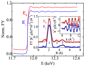
Fig. 1 shows for the 0.6 ML sample the fluorescent yield (FY) versus photon energy for both geometries which is proportional to the linear absorption coefficient. The inspection of the figure reveals that both curves are nearly identical. The detailed analysis was carried out by background subtraction and calculation of the Fourier-Transform (FT) of the k2-weighted interference function [], which are shown in the inset.
The FT magnitude shows three peaks labelled by 1, 2 and 3 for E∥, but only 1 and 3 for E⟂. Peak 1 corresponds to the first selenium shell, while peaks 2 and 3 are related to bismuth shells. For the present discussion we focus on the first shell, which was fitted in R-space using theoretical scattering amplitudes and phases. The fit results are listed in Table 1. In detail, we find that the first peak corresponds to in total six selenium atoms of which three are located at a distance of 2.45 Å and another three at a distance of 2.65 Å (E∥). For E⟂ geometry the distances can be viewed as identical. The structure parameters are compatible with a model, in which gold atoms substitute bismuth atoms.
Comparison of the experimental first shell distances with those in the un-relaxed bulk (R=2.87 Å and R=3.07 Å) indicates substantial local relaxations of the surrounding selenium atoms upon bismuth substitution. This situation closely resembles that of iron deposition on Bi2Se3(0001) Polyakov et al. (2015), where very similar structure parameters have been derived.
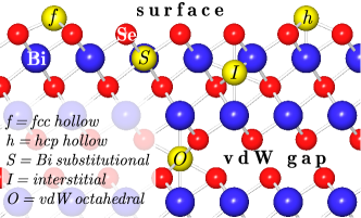
The structure model is discussed on the basis of Fig. 2, where the near surface structure of Bi2Se3 including the first QL is schematically shown. Large (blue) and small (red) spheres represent bismuth and selenium atoms, respectively. The Bi2Se3 crystal structure is characterized by an ABCBA stack of van-der-Waals (vdW) bonded QLs each being composed of a Se-Bi-Se-Bi-Se sequence of layers Roy et al. (2014b). Possible adsorption positions for gold are indicated and are labelled as ”fcc” (f), ”hcp” (h), ”substitutional” (S), ”interstitial”(I) and ”octahedral gap” (O). The absence of any polarization dependence of the peak 1 as well as its relation to a distance in the 2.5 to 2.7 Å range leads to a model where gold atoms are substituting bismuth atoms. Other adsorption sites such as the ”fcc” or ”hcp” sites at the surface or in interstitial sites are not compatible with both the isotropy of the first peak and its relation to a Au-Se bond length.
| Pol. | Sh | Rb(Å) | N | R (Å) | N∗ | (Å2) | E0 (eV) | Ru |
|---|---|---|---|---|---|---|---|---|
| E | Se1 | 2.87 | 3 | 2.45 (3) | 3.04(*) | 0.004 | 2.6 | 4.9 |
| Se2 | 3.07 | 3 | 2.65 (4) | 2.92(*) | 0.014 | 2.6 | ||
| E | Se1 | 2.87 | 3 | 2.44 (3) | 2.92(*) | 0.004 | 3.3 | 2.3 |
| Se2 | 3.07 | 3 | 2.66 (4) | 3.16(*) | 0.021 | 3.3 |
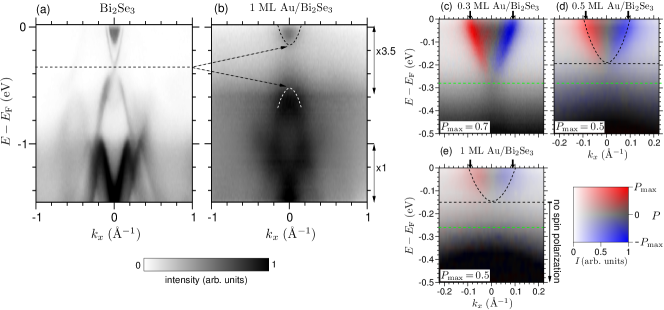
Spin-resolved photoemission experiments were carried out using a momentum microscope (MM) Tusche et al. (2015) equipped with a 2D imaging spin filter based on low-energy electron diffraction at 1 ML Au/Ir(001) Vasilyev et al. (2015). Sample preparation which closely followed the procedure employed for the EXAFS experiments and experimental details are reported in the Supplementary Materials. The photoemission spectra collected by the MM for pristine and gold-covered Bi2Se3 (0001) are displayed along the direction in Fig. 3(a-e), respectively. In the case of the pristine Bi2Se3 sample [Fig. 3(a)], the DP is located approximately 350 meV below resulting from doping by selenium vacancies. After deposition of 1 ML of gold [Fig. 3(b)], the TSS is strongly broadened by the structural disorder introduced by the randomly distributed gold atoms on Bi sites.
More details are derived by spin-resolved spectra collected for 0.3, 0.5 and 1 ML as shown in Figs. 3(b-e). Here, the characteristic spin-momentum locking of the surface state is observed. Gold deposition induces an upwards shift (p-doping) and -more importantly- an opening of the gap which amounts to about 100 meV. The surface state dispersion is not observed to continue into the energy range below the black dashed lines where the two spin-polarized branches meet at [see Fig. 3(d,e)]. The experimental findings are well reproduced by ab-initio calculations as discussed in the following.
First-principles calculations of Au/Bi2Se3 (0001) model gold induced modifications of the TSS. We used a self-consistent full relativistic Green function method especially designed for semi-infinite materials such as surfaces and interfaces Lüders et al. (2001); Geilhufe et al. (2015b). Alloying the bismuth layers with gold was simulated within a coherent potential approximation as implemented within the multiple scattering theory Soven (1967); Gyorffy (1972). The structural information was adopted from the EXAFS experiments (see Table 1).
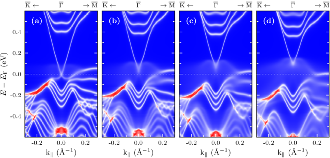
In order to trace the evolution of the TSS upon gold concentration the -resolved spectral density was calculated in (Bi1-xAux)2Se3 on the Bi2Se3(0001) surface for direction in SBZ at concentrations (see (Fig. 4(a-d), respectively). In all these cases Au is assumed to be homogeneously distributed over the Bi sites within the first QL. The results are shown in Fig. 4, where low, medium and high spectral density is represented by blue, white and red color coding, respectively. At [see Fig. 4(a)], the spectral density is similar to that of the pristine Bi2Se3 (0001) surface (not shown), but some broadening is seen in the vicinity of EF, which is attributed to a gold resonance state.
The most important result is that gold substitution induces the formation of a gap of E=200 meV, in a good agreement with photoemission spectra. Within the gap regime the spectral density is considerably weakened due to the presence of a resonance state and because of band broadening induced by structural disorder. Furthermore, gold acts as a p-dopant shifting the bands up in energy. Comparison of the calculated band structure of the pristine surface (not shown here) and the alloyed sample indicate an upward shift of the bands by approximately 330 meV (at ).
Our study provides new insight into the non-magnetic impurity mediated modification of the TSS. Gold atoms deposited in the sub- to one monolayer range on Bi2Se3(0001) occupy substitutional bismuth sites as evidenced by EXAFS measurements. This goes in parallel with the dramatic weakening of the spectral density of the TSS, thus opening a gap as observed by photoemission. In accordance with first-principles calculations, gold in bismuth substitutional site within the first QL creates a d-type resonant state near the , which strongly hybridizes with the bands of the TI and substantially modifies its surface electronic structure. The surface alloy involving only the topmost QL is sufficient for the gap opening, which we attribute to the fact that the resonance state near EF is of -symmetry. According to the model of Black-Schaffer and Balatsky Biswas and Balatsky (2010); Black-Schaffer and Balatsky (2012a, b) a bulk-surface interaction is a prerequisite for the opening of the gap, since the TSS is not protected by scattering processes involving bulk three-dimensional states.
We acknowledge financial support from DFG through priority program SPP1666 (Topological Insulators), the Spanish Ministry of Science and Innovation (Grants No. FIS2013-48286-C02-02-P and No. FIS2013-48286-C02-01-P), the Basque Government through the Nanomaterials project under the nanoGUNE2014 program (Grant No. IE05-151), the Tomsk State University Academic D. I. Mendeleev Fund Program in 2015 (Research Grant No. 8.1.05.2015), and partial support from Saint Petersburg State University (Project No. 15.61.202.2015). Technical support by F. Weiss is gratefully acknowledged. We also thank Z.S. Aliev, M. B. Babanly, K. A. Kokh, and O. E. Tereshchenko for support by providing samples. M.E. acknowledges support from the BMBF (Grant No. 05K12EF1). E.D.C. acknowledges research grants from the Dean, Faculty of Science, Simon Fraser University, and from NSERC. Sector 20 facilities at the Advanced Photon Source, and research at these facilities, are supported by the US Department of Energy - Basic Energy Sciences, the Canadian Light Source and its funding partners, and the Advanced Photon Source. Use of the Advanced Photon Source, an Office of Science User Facility operated for the U.S. Department of Energy (DOE) Office of Science by Argonne National Laboratory, was supported by the U.S. DOE under Contract No. DE-AC02-06CH11357. M.G. acknowledges European Research Council under the European Union’s Seventh Framework Program (FP/2207-2013)/ERC Grant Agreement No. DM-321031.
References
- Hasan and Kane (2010) M. Z. Hasan and C. L. Kane, Rev. Mod. Phys. 82, 3045 (2010).
- Wehling et al. (2014) T. O. Wehling, A. M. Black-Schaffer, and A. V. Balatsky, Advances in Physics 63, 1 (2014).
- Roushan et al. (2009) P. Roushan, J. Seo, C. V. Parker, Y. S. Hor, D. Hsieh, D. Qian, A. Richardella, M. Z. Hasan, R. J. Cava, and A. Yazdani, Nature 460, 1106 (2009).
- Hanaguri et al. (2010) T. Hanaguri, K. Igarashi, M. Kawamura, H. Takagi, and T. Sasagawa, Phys. Rev. B 82, 081305 (2010).
- Alpichshev et al. (2010) Z. Alpichshev, J. G. Analytis, J.-H. Chu, I. R. Fisher, Y. L. Chen, Z. X. Shen, A. Fang, and A. Kapitulnik, Phys. Rev. Lett. 104, 016401 (2010).
- Sessi et al. (2013) P. Sessi, M. M. Otrokov, T. Bathon, M. G. Vergniory, S. S. Tsirkin, K. A. Kokh, O. E. Tereshchenko, E. V. Chulkov, and M. Bode, Phys. Rev. B 88, 161407 (2013).
- Kuroda et al. (2010) K. Kuroda, M. Ye, A. Kimura, S. V. Eremeev, E. E. Krasovskii, E. V. Chulkov, Y. Ueda, K. Miyamoto, T. Okuda, K. Shimada, et al., Phys. Rev. Lett. 105, 146801 (2010).
- Kuroda et al. (2013) K. Kuroda, M. Ye, E. F. Schwier, M. Nurmamat, K. Shirai, M. Nakatake, S. Ueda, K. Miyamoto, T. Okuda, H. Namatame, et al., Phys. Rev. B 88, 245308 (2013).
- Honolka et al. (2012) J. Honolka, A. A. Khajetoorians, V. Sessi, T. O. Wehling, S. Stepanow, J.-L. Mi, B. B. Iversen, T. Schlenk, J. Wiebe, N. B. Brookes, et al., Phys. Rev. Lett. 108, 256811 (2012).
- Scholz et al. (2012) M. R. Scholz, J. Sánchez-Barriga, D. Marchenko, A. Varykhalov, A. Volykhov, L. V. Yashina, and O. Rader, Phys. Rev. Lett. 108, 256810 (2012).
- Polyakov et al. (2015) A. Polyakov, H. L. Meyerheim, E. D. Crozier, R. A. Gordon, K. Mohseni, S. Roy, A. Ernst, M. G. Vergniory, X. Zubizarreta, M. M. Otrokov, et al., Phys. Rev. B 92, 045423 (2015).
- Chen et al. (2010) Y. L. Chen, J.-H. Chu, J. G. Analytis, Z. K. Liu, K. Igarashi, H.-H. Kuo, X. L. Qi, S. K. Mo, R. G. Moore, D. H. Lu, et al., Science 329, 659 (2010).
- Vergniory et al. (2014) M. G. Vergniory, M. M. Otrokov, D. Thonig, M. Hoffmann, I. V. Maznichenko, M. Geilhufe, X. Zubizarreta, S. Ostanin, A. Marmodoro, J. Henk, et al., Phys. Rev. B 89, 165202 (2014).
- Wray et al. (2011) L. A. Wray, S.-Y. Xu, Y. Xia, D. Hsieh, A. V. Fedorov, Y. S. Hor, R. J. Cava, A. Bansil, H. Lin, and M. Z. Hasan, Nat. Phys. 7, 32 (2011).
- Henk et al. (2012) J. Henk, M. Flieger, I. V. Maznichenko, I. Mertig, A. Ernst, S. V. Eremeev, and E. V. Chulkov, Phys. Rev. Lett. 109, 076801 (2012).
- Otrokov et al. (2015) M. M. Otrokov, E. V. Chulkov, and A. Arnau, Phys. Rev. B 92, 165309 (2015).
- Sessi et al. (2016) P. Sessi, R. R. Biswas, T. Bathon, O. Storz, S. Wilfert, A. Barla, K. A. Kokh, O. E. Tereshchenko, K. Fauth, M. Bode, et al., Nat Commun 7, 12027 (2016).
- Zhu et al. (2011) Z.-H. Zhu, G. Levy, B. Ludbrook, C. N. Veenstra, J. A. Rosen, R. Comin, D. Wong, P. Dosanjh, A. Ubaldini, P. Syers, et al., Phys. Rev. Lett. 107, 186405 (2011).
- Benia et al. (2011) H. M. Benia, C. Lin, K. Kern, and C. R. Ast, Phys. Rev. Lett. 107, 177602 (2011).
- King et al. (2011) P. D. C. King, R. C. Hatch, M. Bianchi, R. Ovsyannikov, C. Lupulescu, G. Landolt, B. Slomski, J. H. Dil, D. Guan, J. L. Mi, et al., Phys. Rev. Lett. 107, 096802 (2011).
- Roy et al. (2014a) S. Roy, H. L. Meyerheim, A. Ernst, K. Mohseni, C. Tusche, M. G. Vergniory, T. V. Menshchikova, M. M. Otrokov, A. G. Ryabishchenkova, Z. S. Aliev, et al., Phys. Rev. Lett. 113, 116802 (2014a).
- Miao et al. (2013) L. Miao, Z. F. Wang, W. Ming, M.-Y. Yao, M. Wang, F. Yang, Y. R. Song, F. Zhu, A. V. Fedorov, Z. Sun, et al., Proceedings of the National Academy of Sciences 110, 2758 (2013).
- Menshchikova et al. (2013) T. V. Menshchikova, M. M. Otrokov, S. S. Tsirkin, D. A. Samorokov, V. V. Bebneva, A. Ernst, V. M. Kuznetsov, and E. V. Chulkov, Nano Lett. 13, 6064 (2013).
- Shokri et al. (2015) R. Shokri, H. L. Meyerheim, S. Roy, K. Mohseni, A. Ernst, M. M. Otrokov, E. V. Chulkov, and J. Kirschner, Phys. Rev. B 91, 205430 (2015).
- Liu et al. (2014) Y. Liu, Y. Y. Li, S. Rajput, D. Gilks, L. Lari, P. L. Galindo, M. Weinert, V. K. Lazarov, and L. Li, Nat Phys 10, 294 (2014).
- Geilhufe et al. (2015a) M. Geilhufe, S. K. Nayak, S. Thomas, M. Däne, G. S. Tripathi, P. Entel, W. Hergert, and A. Ernst, Phys. Rev. B 92, 235203 (2015a).
- Sanchez-Barriga et al. (2016) J. Sanchez-Barriga, A. Varykhalov, G. Springholz, H. Steiner, R. Kirchschlager, G. Bauer, O. Caha, E. Schierle, E. Weschke, A. A. Unal, et al., Nat. Commun. 7, 10559 (2016).
- Biswas and Balatsky (2010) R. R. Biswas and A. V. Balatsky, Phys. Rev. B 81, 233405 (2010).
- Black-Schaffer and Balatsky (2012a) A. M. Black-Schaffer and A. V. Balatsky, Phys. Rev. B 85, 121103 (2012a).
- Black-Schaffer and Balatsky (2012b) A. M. Black-Schaffer and A. V. Balatsky, Phys. Rev. B 86, 115433 (2012b).
- Chotorlishvili et al. (2014) L. Chotorlishvili, A. Ernst, V. K. Dugaev, A. Komnik, M. G. Vergniory, E. V. Chulkov, and J. Berakdar, Phys. Rev. B 89, 075103 (2014).
- Gordon et al. (2007) R. A. Gordon, E. D. Crozier, D.-T. Jiang, J. Shoults, B. Barg, and P. S. Budnik, AIP Conference Proceedings 882, 887 (2007).
- Jiang and Crozier (1998) D. T. Jiang and E. D. Crozier, Canadian Journal of Physics 76, 621 (1998).
- Roy et al. (2014b) S. Roy, H. L. Meyerheim, K. Mohseni, A. Ernst, M. M. Otrokov, M. G. Vergniory, G. Mussler, J. Kampmeier, D. Grützmacher, C. Tusche, et al., Phys. Rev. B 90, 155456 (2014b).
- Citrin (1985) P. H. Citrin, Phys. Rev. B 31, 700 (1985).
- (36) The unweighted residuum (Ru) is defined by: R, where Yobs and Ycalc are the experimental and calculated magnitudes of the peak selected in the FT of the spectrum and the summation extends over all points in the window used to filter the peak.
- Tusche et al. (2015) C. Tusche, A. Krasyuk, and J. Kirschner, Ultramicroscopy 159, 520 (2015).
- Vasilyev et al. (2015) D. Vasilyev, C. Tusche, F. Giebels, H. Gollisch, R. Feder, and J. Kirschner, Journal of Electron Spectroscopy and Related Phenomena 199, 10 (2015).
- Lüders et al. (2001) M. Lüders, A. Ernst, W. M. Temmerman, Z. Szotek, and P. J. Durham, Journal of Physics: Condensed Matter 13, 8587 (2001).
- Geilhufe et al. (2015b) M. Geilhufe, S. Achilles, M. A. Köbis, M. Arnold, I. Mertig, W. Hergert, and A. Ernst, Journal of Physics: Condensed Matter 27, 435202 (2015b).
- Soven (1967) P. Soven, Phys. Rev. 156, 809 (1967).
- Gyorffy (1972) B. L. Gyorffy, Phys. Rev. B 5, 2382 (1972).
Appendix A Supplementary material
A.1 Photoemission experiment
Gold was deposited at T=223 K, followed by a mild annealing at 243 K for 5 minutes, the latter improving the structural order, but without inducing in-diffusion of gold in the bulk as in the main text.
For the spin ntegrated photoemission measurements, the Au/Bi2Se3 (0001) sample was illuminated by He-I radiation (21.2 eV) under an angle of incidence of 22∘ with respect to the sample surface, and the azimuth along the direction in the surface Brillouin zone (SBZ). Photoelectrons emitted into the complete solid angle above the sample surface (emission angles of ) were collected by the objective lens of a photoelectron momentum microscope. The image of the photoemission intensity as function of the lateral crystal momentum (kx,ky) is obtained in the focal plane of the objective lens not requiring any sample movement. Series of constant energy momentum images in steps of 10 meV were recorded by a CCD camera from a fluorescent screen image detector.For the spin-resolved photoemission experiments we introduce a 2D imaging spin filter based on low-energy electron diffraction at 1 ML Au/Ir(001) into the momentum microscope. For the spin resolved measurements shown in Fig. 3c-d (main text), the sample was illuminated by 6.0 eV s-polarized laser radiation from the 4th harmonic of a Ti:Sa oscillator, incident along the direction of the SBZ.
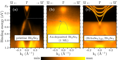
First, the surface band structure of 1 ML gold substituted into bismuth sites and distributed over several QL’s in the surface vicinity was calculated. Since the layer-resolved occupancy of Bi sites by 1ML Au was not known from the experiment, we tried several configurations comparing the calculated electronic structures with the photoemission experiment. A good agreement was achieved for the case of Au distributed over the first two QL’s with concentrations x=0.35,0.25,0.25,0.15 in the first four Bi layers, respectively. The calculated electronic structure shown in Fig. 5(c) agrees well with the experimental photoemission spectra (see Fig. 5(b)). The most important result is that gold substitution induces the formation of a gap of E=0.2 eV, which is in a good agreement with the photoemission experiment. The spectral density is considerably weakened due to the presence of a resonance state and because of band broadening induced by structural disorder. Furthermore, gold acts as a p-dopant shifting the bands up in energy. Comparison of the calculated band structure of the pristine surface (not shown here) and the alloyed sample indicate an upward shift of the bands by approximately 0.33 eV (at x=0.5).
The photoemission spectra collected by the MM for pristine and gold-covered Bi2Se3 (0001) are displayed along the direction in Fig. 5(a,b), respectively. In the case of the pristine Bi2Se3 sample [Fig. 5(a)], the DP is located approximately 350 meV below resulting from doping by selenium vacancies. After the deposition of gold equivalent to one ML [Fig. 5(b)], the TSS is strongly broadened by the structural disorder introduced by the randomly distributed gold atoms on Bi sites, which affects the TSS, as seen in in the calculated spectrum [Fig. 5(c), see the discussion below]. The photoemission process itself is additionally affected by this disorder, leading to a higher background intensity. Therefore, the intensity of the TSS above the DP is too much weakened to be observed. At lower energies than the DP, however, the broadened TSS feature is still observed. As indicated schematically in Figs. 5(a,b), the original dispersion of the TSS below the DP is shifted to lower energies, consistent with the formation of a gap.
While the photoemission peak near in Fig. 3(b) (main text) looks similar to the bulk bands near in Fig. 3(a), the spin-resolved spectra for 0.3, 0.5 and 1 ML Au/Bi2Se3 in Fig. 3(c-e) show the characteristic spin momentum locking of the surface state (opposite spin polarization for ). Upon the deposition of gold, several effects are observed. First, the dispersion of the spin polarized surface state is energetically compressed instead of being shifted [note the small black arrows in Fig. 3(c-e) indicating that the -diameter at is not varying as much as would result from a shift of the surface-state dispersion]. Second, the spin polarization is conserved after the gold deposition. This means that the surface state is not destroyed but modified. The surface state dispersion is not observed to continue in the energy range below the black dashed lines where the two spin-polarized branches meet at [see Fig. 3(d,e)]. In the same energy range, the spin polarization vanishes. Contrarily, for a clean Bi2Se3, the surface state is known to be spin-polarized below the Dirac point. These observations support our interpretation in terms of a gap opening.
A.2 Impurity states in Au/Bi2Se3 (0001)
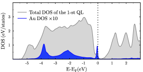
The corresponding density of states (DOS) for x=0.0125 is shown in Fig. 6, where the blue (dark) partial DOS represent the contribution of gold to the total DOS (bright). The resonance is clearly seen near EF. This resonance state is of -character and present in (Bi1-xAux)2Se3 throughout the whole concentration range investigated (). Owing to the -symmetry of the resonance state it is very effective regarding the modification of the TSS since it is related to a strong hybridization with the semiconductor states. With increasing gold concentration the DP is split off from EF and a gap appears. The size of the gap is increasing with the gold concentration (x) and approaches the maximum value of E=150 meV at .