[subfigure]position=top

Strain-enhanced optical absorbance of topological insulator films

Mathias Rosdahl Brems Technical University of Denmark, Department of Photonics Engineering, Kgs. Lyngby, 2800, Denmark    Jens Paaske Center for Quantum Devices, Niels Bohr Institute, University of Copenhagen, Universitetsparken 5, DK-2100 Copenhagen, Denmark    Anders Mathias Lunde Center for Quantum Devices, Niels Bohr Institute, University of Copenhagen, Universitetsparken 5, DK-2100 Copenhagen, Denmark    Morten Willatzen Technical University of Denmark, Department of Photonics Engineering, Kgs. Lyngby, 2800, Denmark
Abstract

Topological insulator films are promising materials for optoelectronics due to a strong optical absorption and a thickness dependent band gap of the topological surface states. They are superior candidates for photodetector applications in the THz-infrared spectrum, with a potential performance higher than graphene. Using a first-principles kp𝑘𝑝k\cdot p Hamiltonian, incorporating all symmetry-allowed terms to second order in the wave vector k𝑘k, first order in the strain ϵitalic-ϵ\epsilon and of order ϵkitalic-ϵ𝑘\epsilon k, we demonstrate significantly improved optoelectronic performance due to strain. For Bi2Se3 films of variable thickness, the surface state band gap, and thereby the optical absorption, can be effectively tuned by application of uniaxial strain, ϵzzsubscriptitalic-ϵ𝑧𝑧\epsilon_{zz}, leading to a divergent band edge absorbance for ϵzz6%greater-than-or-equivalent-tosubscriptitalic-ϵ𝑧𝑧percent6\epsilon_{zz}\gtrsim 6\%. Shear strain breaks the crystal symmetry and leads to an absorbance varying significantly with polarization direction. Remarkably, the directional average of the absorbance always increases with strain, independent of material parameters.

Three-dimensional topological insulators (TI) like Bi2Se3, Bi2Te3 and Sb2Te3 have relatively large inverted band gaps of the order of 0.3 eV and thus host robust topological surface states (TSS) Zhang et al. (2009); Liu et al. (2010) whose Dirac cone band structures have been studied extensively using angle resolved photoemission spectroscopy Zhang et al. (2010); Chen et al. (2009); Xia et al. (2009); Sakamoto et al. (2010). These are layered materials with van der Waals bonded quintuple layers (QL) and can be exfoliated to produce thin TI films for which TSS on opposite surfaces overlap and gap out the respective Dirac cones. Already for a 6 QL film, these Dirac gaps are unobservably small and the film effectively reverts to ordinary 3D-TI behavior Zhang et al. (2010a).

Zhang et al. Zhang et al. (2010b) pointed out that TI films should be promising materials for optoelectronics applications, with an optical absorbance due to the TSS comparable to that of graphene (πα2.3%𝜋𝛼percent2.3\pi\alpha\approx 2.3\% given in terms of the fine structure constant α=e2/(4πϵ0c)1/137𝛼superscript𝑒24𝜋subscriptitalic-ϵ0Planck-constant-over-2-pi𝑐1137\alpha=e^{2}/(4\pi\epsilon_{0}\hbar c)\approx 1/137), roughly two orders of magnitude higher than conventional photodetector materials like Hg1-xCdxTe. One surface of a TI film hosts only a single gapless Dirac cone, which gives rise to a frequency independent total absorbance of πα/2𝜋𝛼2\pi\alpha/2. For thin (less-than-or-similar-to\lesssim 6 QL) TI films, the gapped Dirac electrons may enhance this up to πα𝜋𝛼\pi\alpha and even larger, for frequencies close to the TSS band gap. Breaking inversion symmetry of a thin TI film shifts the minimum Dirac gap to finite wave vectors Shan et al. (2010) and a Mexican-hat shape of the surface state conduction band gives rise to a Van Hove singularity in the joint density of states (JDOS), leading to a divergent band edge absorption and tunability of the two-photon absorption spectrum Wang et al. (2013). Furthermore, the hexagonal warping in the TSS bandstructure has been shown to enhance the optical absorbance above the TSS band gap relevant for higher frequencies Shao et al. (2014). Recent experimental investigations of photocurrent response have indeed shown promising optoelectronic functionality for different TI based nano, and hybrid structures Zang et al. (2014); Sharma et al. (2016); Zheng et al. (2015); Zhang et al. (2014); Qiao et al. (2015); Giorgianni et al. (2016).

In this paper, we investigate the effects of strain on the optical absorption of Bi2Se3 films of variable thickness. We employ the most general Hamiltonian for the Bi2Se3 class of materials, including all symmetry-allowed terms to second order in the wave vector k𝑘k, first order in the strain tensor ϵitalic-ϵ\epsilon and of order ϵkitalic-ϵ𝑘\epsilon k. The detailed derivation of this kp𝑘𝑝k\cdot p Hamiltonian and its surface states, using the method of invariants Lew Yan Voon and Willatzen (2009), will be presented in a separate publication Jensen et al. . Previous theoretical studies of strain on Bi2Se3 were based on density functional theory Luo et al. (2012); Young et al. (2011), and have focused only on the change of the bulk band gap and the possibility of a strain-induced topological phase transition. In contrast, our model Hamiltonian provides deeper insight into the electronic structure and, in particular, how the surface states are affected by strain. To describe the low-energy physics of a thin film, we derive an effective 2D model for the surface states, thus disregarding contributions from the bulk states, which at photon energies in the THz-infrared spectrum (ωsimilar-to𝜔absent\omega~{}\sim 30-300 meV) are expected to be largely negligible Li et al. (2015).

Using this surface-state model together with Fermi’s Golden Rule, we determine the optical absorbance in the presence of strain. Basically, we find that uniaxial strain decreases the bulk band gap and thereby increases the spatial extent of the TSS wave functions, which in turn leads to a larger inter-surface overlap and concomitant energy gap of the TSS. In this way, straining a TI film is perceived by the surface states as making the film thinner, thus enhancing the band-edge absorption studied in Ref. Zhang et al., 2010b. The absorption edge moves to higher frequency, and the absorbance at the edge increases. Increasing the uniaxial strain above 666 %, we find that the minimum TSS band-gap shifts to finite wave vectors. This leads to a Van Hove singularity in the joint density of states (JDOS), resulting in a divergent band edge absorption even in the presence of inversion symmetry. For shear strain or ϵxxϵyysubscriptitalic-ϵ𝑥𝑥subscriptitalic-ϵ𝑦𝑦\epsilon_{xx}\neq\epsilon_{yy} the isotropy of the model is broken, and a strong polarization dependence appears. In an isotropic model the photocurrent is polarization dependent due to the anisotropic excitation in k𝑘k space Yao et al. (2015), and we propose to enhance this effect by strain. Subject to strain, in the thick-film limit where the TSS band gap closes, the absorbance is independent of the photon energy, with a magnitude depending sinusoidally on the polarization angle. Averaging over polarization angle, however, we show that strain always increases the average absorbance above the universal value απ2𝛼𝜋2\frac{\alpha\pi}{2}, independently of material parameters.

Model Hamiltonian. Based on the symmetries of the crystal, we have employed the Method of Invariants to derive the most general kp𝑘𝑝k\cdot p Hamiltonian to second order in wave vector and first order in strain Jensen et al. , given here in the basis Liu et al. (2010) |P1+,12ket𝑃superscriptsubscript112|P1_{-}^{+},\tfrac{1}{2}\rangle, i|P2+,12𝑖ket𝑃superscriptsubscript212-i|P2_{+}^{-},\tfrac{1}{2}\rangle, |P1+,12ket𝑃superscriptsubscript112|P1_{-}^{+},-\tfrac{1}{2}\rangle, i|P2+,12𝑖ket𝑃superscriptsubscript212i|P2_{+}^{-},-\tfrac{1}{2}\rangle by

H3D=0superscript𝐻3𝐷subscript0\displaystyle H^{3D}=\mathcal{E}_{0} +(βiki0αikiβikiαiki00αikiβikiαiki0βiki)matrixsubscriptsuperscript𝛽𝑖subscript𝑘𝑖0subscriptsuperscript𝛼𝑖subscript𝑘𝑖subscript𝛽𝑖subscript𝑘𝑖subscriptsuperscript𝛼𝑖subscript𝑘𝑖00subscript𝛼𝑖subscript𝑘𝑖subscript𝛽𝑖subscript𝑘𝑖subscript𝛼𝑖subscript𝑘𝑖0subscriptsuperscript𝛽𝑖subscript𝑘𝑖\displaystyle+\begin{pmatrix}\mathcal{M}&\beta^{*}_{i}k_{i}&0&\alpha^{*}_{i}k_{i}\\ \beta_{i}k_{i}&-\mathcal{M}&\alpha^{*}_{i}k_{i}&0\\ 0&\alpha_{i}k_{i}&\mathcal{M}&-\beta_{i}k_{i}\\ \alpha_{i}k_{i}&0&-\beta^{*}_{i}k_{i}&-\mathcal{M}\end{pmatrix} (1)

where repeated indices are summed over i=x,y,z𝑖𝑥𝑦𝑧i=x,y,z, and

0(𝐤)subscript0𝐤\displaystyle\mathcal{E}_{0}(\mathbf{k}) =C+C1ϵzz+C2ϵ+D1kz2+D2k2,absent𝐶subscript𝐶1subscriptitalic-ϵ𝑧𝑧subscript𝐶2subscriptitalic-ϵsubscript𝐷1superscriptsubscript𝑘𝑧2subscript𝐷2superscriptsubscript𝑘2\displaystyle=C+C_{1}\epsilon_{zz}+C_{2}\epsilon_{\|}+D_{1}k_{z}^{2}+D_{2}k_{\|}^{2}, (2)
(𝐤)𝐤\displaystyle\mathcal{M}(\mathbf{k}) =M+M1ϵzz+M2ϵB1kz2B2k2,absent𝑀subscript𝑀1subscriptitalic-ϵ𝑧𝑧subscript𝑀2subscriptitalic-ϵsubscript𝐵1superscriptsubscript𝑘𝑧2subscript𝐵2superscriptsubscript𝑘2\displaystyle=M+M_{1}\epsilon_{zz}+M_{2}\epsilon_{\|}-B_{1}k_{z}^{2}-B_{2}k_{\|}^{2}, (3)
αxsubscript𝛼𝑥\displaystyle\alpha_{x} =A2+A21ϵzz+A22ϵ+iY3ϵz+Y4ϵ+,absentsubscript𝐴2subscript𝐴21subscriptitalic-ϵ𝑧𝑧subscript𝐴22subscriptitalic-ϵ𝑖subscript𝑌3subscriptitalic-ϵlimit-from𝑧subscript𝑌4subscriptitalic-ϵ\displaystyle=A_{2}+A_{21}\epsilon_{zz}+A_{22}\epsilon_{\|}+iY_{3}\epsilon_{z-}+Y_{4}\epsilon_{+}, (4)
αysubscript𝛼𝑦\displaystyle\alpha_{y} =iA2+iA21ϵzz+iA22ϵ+Y3ϵziY4ϵ+,absent𝑖subscript𝐴2𝑖subscript𝐴21subscriptitalic-ϵ𝑧𝑧𝑖subscript𝐴22subscriptitalic-ϵsubscript𝑌3subscriptitalic-ϵlimit-from𝑧𝑖subscript𝑌4subscriptitalic-ϵ\displaystyle=iA_{2}+iA_{21}\epsilon_{zz}+iA_{22}\epsilon_{\|}+Y_{3}\epsilon_{z-}-iY_{4}\epsilon_{+}, (5)
αzsubscript𝛼𝑧\displaystyle\alpha_{z} =Y1ϵz++iY2ϵ,absentsubscript𝑌1subscriptitalic-ϵlimit-from𝑧𝑖subscript𝑌2subscriptitalic-ϵ\displaystyle=Y_{1}\epsilon_{z+}+iY_{2}\epsilon_{-}, (6)
βxsubscript𝛽𝑥\displaystyle\beta_{x} =X1ϵzx+2X2ϵxyiX3ϵzy+iX4(ϵxxϵyy),absentsubscript𝑋1subscriptitalic-ϵ𝑧𝑥2subscript𝑋2subscriptitalic-ϵ𝑥𝑦𝑖subscript𝑋3subscriptitalic-ϵ𝑧𝑦𝑖subscript𝑋4subscriptitalic-ϵ𝑥𝑥subscriptitalic-ϵ𝑦𝑦\displaystyle=X_{1}\epsilon_{zx}+2X_{2}\epsilon_{xy}-iX_{3}\epsilon_{zy}+iX_{4}(\epsilon_{xx}-\epsilon_{yy}), (7)
βysubscript𝛽𝑦\displaystyle\beta_{y} =X1ϵzy+X2(ϵxxϵyy)+iX3ϵzx2iX4ϵxy,absentsubscript𝑋1subscriptitalic-ϵ𝑧𝑦subscript𝑋2subscriptitalic-ϵ𝑥𝑥subscriptitalic-ϵ𝑦𝑦𝑖subscript𝑋3subscriptitalic-ϵ𝑧𝑥2𝑖subscript𝑋4subscriptitalic-ϵ𝑥𝑦\displaystyle=X_{1}\epsilon_{zy}+X_{2}(\epsilon_{xx}-\epsilon_{yy})+iX_{3}\epsilon_{zx}-2iX_{4}\epsilon_{xy}, (8)
βzsubscript𝛽𝑧\displaystyle\beta_{z} =A1+A11ϵzz+A12ϵ,absentsubscript𝐴1subscript𝐴11subscriptitalic-ϵ𝑧𝑧subscript𝐴12subscriptitalic-ϵ\displaystyle=A_{1}+A_{11}\epsilon_{zz}+A_{12}\epsilon_{\|}, (9)

with ϵ=ϵxx+ϵyysubscriptitalic-ϵsubscriptitalic-ϵ𝑥𝑥subscriptitalic-ϵ𝑦𝑦\epsilon_{\|}=\epsilon_{xx}+\epsilon_{yy}, ϵ±=ϵxxϵyy±2iϵxysubscriptitalic-ϵplus-or-minusplus-or-minussubscriptitalic-ϵ𝑥𝑥subscriptitalic-ϵ𝑦𝑦2𝑖subscriptitalic-ϵ𝑥𝑦\epsilon_{\pm}=\epsilon_{xx}-\epsilon_{yy}\pm 2i\epsilon_{xy}, ϵz±=ϵzx±ϵzysubscriptitalic-ϵlimit-from𝑧plus-or-minusplus-or-minussubscriptitalic-ϵ𝑧𝑥subscriptitalic-ϵ𝑧𝑦\epsilon_{z\pm}=\epsilon_{zx}\pm\epsilon_{zy}, and 𝐤=(𝐤,kz)𝐤subscript𝐤subscript𝑘𝑧{\bf k}=({\bf k}_{\|},k_{z}). All capital roman letters denote real parameters of the model, which are not determined by the symmetries of the crystal.

For an infinite slab in the xy𝑥𝑦xy plane, with a finite thickness L𝐿L in the z𝑧z direction, we impose hard-wall boundary conditions at the surfaces located at ±L/2plus-or-minus𝐿2\pm L/2. The full Hamiltonian can be split into two parts H3D(𝐤)=H0(kz)+ΔH(𝐤)superscript𝐻3𝐷𝐤subscript𝐻0subscript𝑘𝑧Δ𝐻𝐤H^{3D}(\mathbf{k})=H_{0}(k_{z})+\Delta H(\mathbf{k}), with H0(kz)subscript𝐻0subscript𝑘𝑧H_{0}(k_{z}) containing all constant terms, kzsubscript𝑘𝑧k_{z} up to second order and first order strain terms and ΔH(𝐤)Δ𝐻𝐤\Delta H(\mathbf{k}) containing terms first and second order in 𝐤||\mathbf{k}_{||} and of order ϵ𝐤italic-ϵ𝐤\epsilon\mathbf{k}. Treating ΔH(𝐤)Δ𝐻𝐤\Delta H(\mathbf{k}) as a perturbation, we first solve H0(kz)subscript𝐻0subscript𝑘𝑧H_{0}(k_{z}) giving the eigenstates  Shan et al. (2010)

Ψ±(z)=(ϕ±(z),0),Ψ±(z)=(0,τzϕ±(z)),formulae-sequencesubscriptsuperscriptΨplus-or-minus𝑧subscriptitalic-ϕplus-or-minus𝑧0subscriptsuperscriptΨplus-or-minus𝑧0subscript𝜏𝑧subscriptitalic-ϕplus-or-minus𝑧\displaystyle\Psi^{\uparrow}_{\pm}(z)=\left(\phi_{\pm}(z),0\right),\quad\Psi^{\downarrow}_{\pm}(z)=\left(0,\tau_{z}\phi_{\pm}(z)\right), (10)

where τisubscript𝜏𝑖\tau_{i} denotes the Pauli matrices and

ϕ±(z)subscriptitalic-ϕplus-or-minus𝑧\displaystyle\phi_{\pm}(z) =C±((D1+B1)η±φ±(z),iA1φ(z)).absentsubscript𝐶plus-or-minussubscript𝐷1subscript𝐵1subscript𝜂plus-or-minussubscript𝜑plus-or-minus𝑧𝑖subscript𝐴1subscript𝜑minus-or-plus𝑧\displaystyle=C_{\pm}\left((D_{1}+B_{1})\eta_{\pm}\varphi_{\pm}(z),iA_{1}\varphi_{\mp}(z)\right). (11)

Here C±subscript𝐶plus-or-minusC_{\pm} are normalization constants, and

η±subscript𝜂plus-or-minus\displaystyle\eta_{\pm} =λ22λ12λ1ϱ(λ1L2)/ϱ±(λ1L2)λ2ϱ(λ2L2)/ϱ±(λ2L2),absentsuperscriptsubscript𝜆22superscriptsubscript𝜆12subscript𝜆1subscriptitalic-ϱminus-or-plussubscript𝜆1𝐿2subscriptitalic-ϱplus-or-minussubscript𝜆1𝐿2subscript𝜆2subscriptitalic-ϱminus-or-plussubscript𝜆2𝐿2subscriptitalic-ϱplus-or-minussubscript𝜆2𝐿2\displaystyle=\frac{\lambda_{2}^{2}-\lambda_{1}^{2}}{\lambda_{1}\varrho_{\mp}(\frac{\lambda_{1}L}{2})/\varrho_{\pm}(\frac{\lambda_{1}L}{2})-\lambda_{2}\varrho_{\mp}(\frac{\lambda_{2}L}{2})/\varrho_{\pm}(\frac{\lambda_{2}L}{2})},
φ±(z)subscript𝜑plus-or-minus𝑧\displaystyle\varphi_{\pm}(z) =(ϱ±(λ1z)ϱ±(λ1L2)ϱ±(λ2z)ϱ±(λ2L2)),absentsubscriptitalic-ϱplus-or-minussubscript𝜆1𝑧subscriptitalic-ϱplus-or-minussubscript𝜆1𝐿2subscriptitalic-ϱplus-or-minussubscript𝜆2𝑧subscriptitalic-ϱplus-or-minussubscript𝜆2𝐿2\displaystyle=\left(\frac{\varrho_{\pm}(\lambda_{1}z)}{\varrho_{\pm}(\frac{\lambda_{1}L}{2})}-\frac{\varrho_{\pm}(\lambda_{2}z)}{\varrho_{\pm}(\frac{\lambda_{2}L}{2})}\right), (12)

with ϱ±(x)=(ex±ex)/2subscriptitalic-ϱplus-or-minus𝑥plus-or-minussuperscript𝑒𝑥superscript𝑒𝑥2\varrho_{\pm}(x)=(e^{x}\pm e^{-x})/2 encoding hyperbolic sines and cosines, and λα=(((1)αRF)/(2D+D))1/2subscript𝜆𝛼superscriptsuperscript1𝛼𝑅𝐹2subscript𝐷subscript𝐷12\lambda_{\alpha}=(((-1)^{\alpha}\sqrt{R}-F)/(2D_{+}D_{-}))^{1/2}, where

F𝐹\displaystyle F =|A1|2+2((E𝐤=0)D1𝐤=0B1),absentsuperscriptsubscript𝐴122𝐸subscript𝐤0subscript𝐷1subscript𝐤0subscript𝐵1\displaystyle=|A_{1}|^{2}+2((E-\mathcal{E}_{\mathbf{k}=0})D_{1}-\mathcal{M}_{\mathbf{k}=0}B_{1}), (13)
R𝑅\displaystyle R =F2+4D+D(𝐤=02(E𝐤=0)2),absentsuperscript𝐹24subscript𝐷subscript𝐷superscriptsubscript𝐤02superscript𝐸subscript𝐤02\displaystyle=F^{2}+4D_{+}D_{-}(\mathcal{M}_{\mathbf{k}=0}^{2}-(E-\mathcal{E}_{\mathbf{k}=0})^{2}), (14)

with D±=D1±B1subscript𝐷plus-or-minusplus-or-minussubscript𝐷1subscript𝐵1D_{\pm}=D_{1}\pm B_{1}. To obtain an effective 2D model for the surface states we project H3D(𝐤)superscript𝐻3𝐷𝐤H^{3D}(\mathbf{k}) into the surface state basis {|Ψ,|Ψ+,|Ψ+,|Ψ}ketsuperscriptsubscriptΨketsuperscriptsubscriptΨketsuperscriptsubscriptΨketsuperscriptsubscriptΨ\left\{|\Psi_{-}^{\uparrow}\rangle,|\Psi_{+}^{\downarrow}\rangle,|\Psi_{+}^{\uparrow}\rangle,|\Psi_{-}^{\downarrow}\rangle\right\} of H0(kz)subscript𝐻0subscript𝑘𝑧H_{0}(k_{z}), thus excluding contributions from the bulk states:

H2D=E¯0+D¯k2superscript𝐻2𝐷subscript¯𝐸0¯𝐷superscriptsubscript𝑘2\displaystyle H^{2D}=\bar{E}_{0}+\bar{D}k_{\|}^{2}
+(M¯+B¯k2α¯ikiβ¯iki0α¯ikiM¯B¯k20β¯ikiβ¯iki0M¯B¯k2α¯iki0β¯ikiα¯ikiM¯+B¯k2),matrix¯𝑀¯𝐵superscriptsubscript𝑘2superscriptsubscript¯𝛼𝑖subscript𝑘𝑖subscript¯𝛽𝑖subscript𝑘𝑖0subscript¯𝛼𝑖subscript𝑘𝑖¯𝑀¯𝐵superscriptsubscript𝑘20subscript¯𝛽𝑖subscript𝑘𝑖subscriptsuperscript¯𝛽𝑖subscript𝑘𝑖0¯𝑀¯𝐵superscriptsubscript𝑘2superscriptsubscript¯𝛼𝑖subscript𝑘𝑖0subscriptsuperscript¯𝛽𝑖subscript𝑘𝑖subscript¯𝛼𝑖subscript𝑘𝑖¯𝑀¯𝐵superscriptsubscript𝑘2\displaystyle+\begin{pmatrix}\bar{M}+\bar{B}k_{\|}^{2}&\bar{\alpha}_{i}^{*}k_{i}&\bar{\beta}_{i}k_{i}&0\\ \bar{\alpha}_{i}k_{i}&-\bar{M}-\bar{B}k_{\|}^{2}&0&\bar{\beta}_{i}k_{i}\\ \bar{\beta}^{*}_{i}k_{i}&0&-\bar{M}-\bar{B}k_{\|}^{2}&-\bar{\alpha}_{i}^{*}k_{i}\\ 0&\bar{\beta}^{*}_{i}k_{i}&-\bar{\alpha}_{i}k_{i}&\bar{M}+\bar{B}k_{\|}^{2}\end{pmatrix},

where repeated indices are summed over i=x,y𝑖𝑥𝑦i=x,y. The parameters of the 2D model, denoted with a bar, now depend on thickness, L𝐿L, and are related to the strain-dependent parameters of the 3D model by:

E¯0subscript¯𝐸0\displaystyle\bar{E}_{0} =E+0+E02,absentsubscriptsuperscript𝐸0subscriptsuperscript𝐸02\displaystyle=\frac{E^{0}_{+}+E^{0}_{-}}{2}, (16)
M¯¯𝑀\displaystyle\bar{M} =E0E+02,absentsubscriptsuperscript𝐸0subscriptsuperscript𝐸02\displaystyle=\frac{E^{0}_{-}-E^{0}_{+}}{2}, (17)
D¯¯𝐷\displaystyle\bar{D} =D2+ϕ+|τz|ϕ++ϕ|τz|ϕ2B2,absentsubscript𝐷2quantum-operator-productsubscriptitalic-ϕsubscript𝜏𝑧subscriptitalic-ϕquantum-operator-productsubscriptitalic-ϕsubscript𝜏𝑧subscriptitalic-ϕ2subscript𝐵2\displaystyle=D_{2}+\frac{\langle\phi_{+}|\tau_{z}|\phi_{+}\rangle+\langle\phi_{-}|\tau_{z}|\phi_{-}\rangle}{2}B_{2}, (18)
B¯¯𝐵\displaystyle\bar{B} =ϕ+|τz|ϕ+ϕ|τz|ϕ2B2,absentquantum-operator-productsubscriptitalic-ϕsubscript𝜏𝑧subscriptitalic-ϕquantum-operator-productsubscriptitalic-ϕsubscript𝜏𝑧subscriptitalic-ϕ2subscript𝐵2\displaystyle=\frac{\langle\phi_{+}|\tau_{z}|\phi_{+}\rangle-\langle\phi_{-}|\tau_{z}|\phi_{-}\rangle}{2}B_{2}, (19)
α¯isubscript¯𝛼𝑖\displaystyle\bar{\alpha}_{i} =iϕ+|τy|ϕαi,absent𝑖quantum-operator-productsubscriptitalic-ϕsubscript𝜏𝑦subscriptitalic-ϕsubscript𝛼𝑖\displaystyle=i\langle\phi_{+}|\tau_{y}|\phi_{-}\rangle\alpha_{i}, (20)
β¯isubscript¯𝛽𝑖\displaystyle\bar{\beta}_{i} =ϕ+|τx|ϕRe[βi]+iϕ+|τy|ϕiIm[βi],absentquantum-operator-productsubscriptitalic-ϕsubscript𝜏𝑥subscriptitalic-ϕResubscript𝛽𝑖𝑖quantum-operator-productsubscriptitalic-ϕsubscript𝜏𝑦subscriptitalic-ϕ𝑖Imsubscript𝛽𝑖\displaystyle=\langle\phi_{+}|\tau_{x}|\phi_{-}\rangle\operatorname{Re}[\beta_{i}]+i\langle\phi_{+}|\tau_{y}|\phi_{-}\rangle i\operatorname{Im}[\beta_{i}], (21)

where E±0subscriptsuperscript𝐸0plus-or-minusE^{0}_{\pm} are the eigenenergies of H0(kz)subscript𝐻0subscript𝑘𝑧H_{0}(k_{z}). From this, we obtain an effective 2D model and derive the spectrum for TSS on a strained TI film:

E±(𝐤)=E¯0+D¯k2±12ΔE𝐤,subscript𝐸plus-or-minussubscript𝐤plus-or-minussubscript¯𝐸0¯𝐷superscriptsubscript𝑘212Δsubscript𝐸subscript𝐤\displaystyle E_{\pm}({\mathbf{k}}_{\|})={\bar{E}}_{0}+{\bar{D}}k_{\|}^{2}\pm\frac{1}{2}\Delta E_{{\mathbf{k}}_{\|}}, (22)

with ΔE𝐤=2|α¯iki|2+|β¯iki|2+(M¯+B¯k2)2Δsubscript𝐸subscript𝐤2superscriptsubscript¯𝛼𝑖subscript𝑘𝑖2superscriptsubscript¯𝛽𝑖subscript𝑘𝑖2superscript¯𝑀¯𝐵superscriptsubscript𝑘22\Delta E_{{\mathbf{k}}_{\|}}=2\sqrt{|\bar{\alpha}_{i}k_{i}|^{2}+|\bar{\beta}_{i}k_{i}|^{2}+(\bar{M}+\bar{B}k_{\|}^{2})^{2}}. From the latter result, we obtain the surface state band gap at
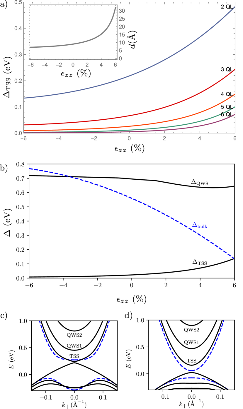
 k=0subscript𝑘0k_{\|}=0

ΔΔ\displaystyle\Delta =2M¯,absent2¯𝑀\displaystyle=2\bar{M}, (23)

which is plotted in Fig. 1 as a function of the strain component ϵzzsubscriptitalic-ϵ𝑧𝑧\epsilon_{zz} for different numbers of quintuple layers in the film. We note in passing that the bulk band gap ΔbulksubscriptΔ𝑏𝑢𝑙𝑘\Delta_{bulk} of strained Bi2Se3 is given by

ΔbulksubscriptΔ𝑏𝑢𝑙𝑘\displaystyle\Delta_{bulk} =2(M+M1ϵzz+M2ϵ).absent2𝑀subscript𝑀1subscriptitalic-ϵ𝑧𝑧subscript𝑀2subscriptitalic-ϵ\displaystyle=2\left(M+M_{1}\epsilon_{zz}+M_{2}\epsilon_{\|}\right). (24)

In Fig. 1, we also plot, for a 444QL film, the band gaps and bandstructure associated with surface states (TSS) and quantum-well states (QWS). For comparison the bulk band gap and bandstructure are shown as blue dashed lines.

Refer to caption
Figure 1: In the upper plot, we show the surface state band gap ΔΔ\Delta calculated from H3Dsuperscript𝐻3𝐷H^{3D} for a slab geometry with 26262-6 QL, using the parameters from Ref. Liu et al., 2010 and the dependence of the bulk band gap with strain from Ref. Young et al., 2011. The inset shows the expectation value of the distance d𝑑d to the surface of a semi-infinite slab vs. ϵzzsubscriptitalic-ϵ𝑧𝑧\epsilon_{zz} for a surface state electron with k=0subscript𝑘0k_{\|}=0. As the surface state extends further into the bulk, the hybridization gap increases. In the middle panel, we plot the band gaps at k=0subscript𝑘parallel-to0k_{\parallel}=0 for a 444QL film associated with surface states (TSS), quantum-well states (QWS), and, for comparison, also the band gap of bulk Bi2Se3 computed with DFT Young et al. (2011). In the left and right plots of the lower panel, the TSS and QWS bands of a 444QL film are shown for ϵzz=0subscriptitalic-ϵ𝑧𝑧0\epsilon_{zz}=0 and ϵzz=6subscriptitalic-ϵ𝑧𝑧6\epsilon_{zz}=6 %, respectively. For comparison, also the bulk bands are plotted (blue dashed).

Optical absorbance. Within this strained 2D model for the TSS of a thin film, we now calculate the optical absorbance using Fermi’s Golden Rule in the dipole approximation. Here we consider only linearly polarized, normal incident light, corresponding to the vector potential 𝐀(t)=A𝐧^cos(ωt)𝐀𝑡𝐴^𝐧𝜔𝑡\mathbf{A}(t)=A\hat{\bf n}\cos(\omega t) at the surface, where 𝐧^=(cos(θA),sin(θA),0)^𝐧subscript𝜃𝐴subscript𝜃𝐴0\hat{\bf n}=(\cos(\theta_{A}),\sin(\theta_{A}),0) denotes the polarization vector, given in terms of its angle with the x𝑥x-axis, θAsubscript𝜃𝐴\theta_{A}. The interaction with the TSS is obtained by minimal substitution, 𝐤𝐤+e𝐀/𝐤𝐤𝑒𝐀Planck-constant-over-2-pi\mathbf{k}\rightarrow\mathbf{k}+e\mathbf{A}/\hbar, in H2Dsuperscript𝐻2𝐷H^{2D}, which yields the interaction term

Hint=e(0α¯iAiβ¯iAi0α¯iAi00β¯iAiβ¯iAi00α¯iAi0β¯iAiα¯iAi0).subscript𝐻int𝑒Planck-constant-over-2-pimatrix0superscriptsubscript¯𝛼𝑖subscript𝐴𝑖subscript¯𝛽𝑖subscript𝐴𝑖0subscript¯𝛼𝑖subscript𝐴𝑖00subscript¯𝛽𝑖subscript𝐴𝑖subscriptsuperscript¯𝛽𝑖subscript𝐴𝑖00superscriptsubscript¯𝛼𝑖subscript𝐴𝑖0subscriptsuperscript¯𝛽𝑖subscript𝐴𝑖subscript¯𝛼𝑖subscript𝐴𝑖0\displaystyle H_{\text{int}}=\frac{e}{\hbar}\begin{pmatrix}0&\bar{\alpha}_{i}^{*}A_{i}&\bar{\beta}_{i}A_{i}&0\\ \bar{\alpha}_{i}A_{i}&0&0&\bar{\beta}_{i}A_{i}\\ \bar{\beta}^{*}_{i}A_{i}&0&0&-\bar{\alpha}_{i}^{*}A_{i}\\ 0&\bar{\beta}^{*}_{i}A_{i}&-\bar{\alpha}_{i}A_{i}&0\end{pmatrix}. (25)

The Golden Rule rate for direct transitions between negative and positive energy surface states is given by

ΓΓ\displaystyle\Gamma =2π𝐤,i,f|f|Hint|i|2δ(ωΔE𝐤),absent2𝜋Planck-constant-over-2-pisubscriptsubscript𝐤𝑖𝑓superscriptquantum-operator-product𝑓subscript𝐻int𝑖2𝛿Planck-constant-over-2-pi𝜔Δsubscript𝐸subscript𝐤\displaystyle=\frac{2\pi}{\hbar}\sum_{{\mathbf{k}}_{\|},i,f}|\langle f|H_{\text{int}}|i\rangle|^{2}\delta(\hbar\omega-\Delta E_{{\mathbf{k}}_{\|}}), (26)

and the absorbance, 𝒫𝒫\mathcal{P}, is found as the ratio of absorbed, Γω/AreaΓPlanck-constant-over-2-pi𝜔Area\Gamma\hbar\omega/\text{Area}, to incident intensity, 12cϵ0ω2|A|212𝑐subscriptitalic-ϵ0superscript𝜔2superscript𝐴2\frac{1}{2}c\epsilon_{0}\omega^{2}|A|^{2}, whereby

𝒫(θA)=α202πdθkk0(θk)Im[χ]2+|γ|2+(2ω)2(M¯+B¯k0(θk)2)2Re[χ]2A(θk)2|A(θk)2+2B¯(M¯+B¯k0(θk)2)|.\mathcal{P}(\theta_{A})=\frac{\alpha}{2}\int_{0}^{2\pi}\mathrm{d}\theta_{k}\sum_{k_{0}(\theta_{k})}\\ \frac{\operatorname{Im}[\chi]^{2}+|\gamma|^{2}+(\frac{2}{\hbar\omega})^{2}(\bar{M}+\bar{B}k_{0}(\theta_{k})^{2})^{2}\operatorname{Re}[\chi]^{2}}{A(\theta_{k})^{2}|A(\theta_{k})^{2}+2\bar{B}(\bar{M}+\bar{B}k_{0}(\theta_{k})^{2})|}. (27)

Here the sum runs over solutions to ΔE𝐤=ωΔsubscript𝐸subscript𝐤Planck-constant-over-2-pi𝜔\Delta E_{{\mathbf{k}}_{\|}}=\hbar\omega, with the parametrization 𝐤=k0(cosθk,sinθk)subscript𝐤subscript𝑘0subscript𝜃𝑘subscript𝜃𝑘{\mathbf{k}}_{\|}=k_{0}(\cos\theta_{k},\sin\theta_{k}), given by

k02(θk)=superscriptsubscript𝑘02subscript𝜃𝑘absent\displaystyle k_{0}^{2}(\theta_{k})= 12B¯2(2M¯B¯2A(θk)2\displaystyle\frac{1}{2\bar{B}^{2}}\Big{(}-2\bar{M}\bar{B}_{2}-A(\theta_{k})^{2} (28)
±(2M¯B¯+A(θk)2)2+B¯2(2ω24M¯2)),\displaystyle\pm\sqrt{(2\bar{M}\bar{B}+A(\theta_{k})^{2})^{2}+\bar{B}^{2}(\hbar^{2}\omega^{2}-4\bar{M}^{2})}\Big{)},

with A(θk)=|fα(θk)|2+|fβ(θk)|2𝐴subscript𝜃𝑘superscriptsubscript𝑓𝛼subscript𝜃𝑘2superscriptsubscript𝑓𝛽subscript𝜃𝑘2A(\theta_{k})=\sqrt{|f_{\alpha}(\theta_{k})|^{2}+|f_{\beta}(\theta_{k})|^{2}}, defined in terms of functions fα(θ)=α¯xcos(θ)+α¯ysin(θ)subscript𝑓𝛼𝜃subscript¯𝛼𝑥𝜃subscript¯𝛼𝑦𝜃f_{\alpha}(\theta)=\bar{\alpha}_{x}\cos(\theta)+\bar{\alpha}_{y}\sin(\theta) and fβ(θ)=β¯xcos(θ)+β¯ysin(θ)subscript𝑓𝛽𝜃subscript¯𝛽𝑥𝜃subscript¯𝛽𝑦𝜃f_{\beta}(\theta)=\bar{\beta}_{x}\cos(\theta)+\bar{\beta}_{y}\sin(\theta), and with χ=fα(θk)fα(θA)+fβ(θk)fβ(θA)𝜒subscript𝑓𝛼subscript𝜃𝑘subscriptsuperscript𝑓𝛼subscript𝜃𝐴subscript𝑓𝛽subscript𝜃𝑘subscriptsuperscript𝑓𝛽subscript𝜃𝐴\chi=f_{\alpha}(\theta_{k})f^{\ast}_{\alpha}(\theta_{A})+f_{\beta}(\theta_{k})f^{\ast}_{\beta}(\theta_{A}) and γ=(α¯xβ¯yα¯yβ¯x)sin(θAθk)𝛾subscript¯𝛼𝑥subscript¯𝛽𝑦subscript¯𝛼𝑦subscript¯𝛽𝑥subscript𝜃𝐴subscript𝜃𝑘\gamma=(\bar{\alpha}_{x}\bar{\beta}_{y}-\bar{\alpha}_{y}\bar{\beta}_{x})\sin(\theta_{A}-\theta_{k}).

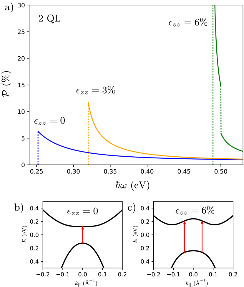
In the case where only the strain components ϵzzsubscriptitalic-ϵ𝑧𝑧\epsilon_{zz} and ϵsubscriptitalic-ϵ\epsilon_{\|} are non-zero, the rotational symmetry in the xy𝑥𝑦xy plane is not broken and Eq. (27) can be integrated analytically. If furthermore the smallest band gap occurs at k=0subscript𝑘0k_{\|}=0, the result from Ref. Zhang et al., 2010b is obtained. However, for M¯B¯+A2(θk)<0¯𝑀¯𝐵superscript𝐴2subscript𝜃𝑘0\bar{M}\bar{B}+A^{2}(\theta_{k})<0, the smallest band gap appears at k0subscript𝑘0k_{\|}\neq 0, which gives rise to a Van Hove singularity in the JDOS causing a divergent absorption edge below the larger band gap at k=0subscript𝑘0k_{\|}=0. As we saw in the previous section, the k=0subscript𝑘0k_{\|}=0 band gap can be significantly increased by application of a tensile uniaxial strain. In Fig. 2 we show the absorption spectrum for ϵzz=0%subscriptitalic-ϵ𝑧𝑧percent0\epsilon_{zz}=0\%, ϵzz=3%subscriptitalic-ϵ𝑧𝑧percent3\epsilon_{zz}=3\%, and ϵzz=6%subscriptitalic-ϵ𝑧𝑧percent6\epsilon_{zz}=6\% for a slab thickness of 222 QL. From 3% to 6% we see the band gap and band-edge absorption increasing. For a strain higher than 6% we find a large absorbance in the energy range between the smallest band gap occurring at k0subscript𝑘0k_{\|}\neq 0 and the k=0subscript𝑘0k_{\|}=0 band gap with a divergence at the former and a discontinuity at the latter. For other thicknesses the change in the band-edge absorbance is similar, but the qualitative change due to the gap occurring at finite wave vector is only observed for 2 QL within a reasonable amount of strain. Also shown in Fig. 2 are the 222QL TSS bandstructure for ϵzz=0subscriptitalic-ϵ𝑧𝑧0\epsilon_{zz}=0 and ϵzz=6subscriptitalic-ϵ𝑧𝑧6\epsilon_{zz}=6 %, respectively.

Refer to caption
Figure 2: Upper panel: The absorbance for a 222 QL slab under tensile uniaxial strain. The absorbance is independent of the light polarization since the isotropy is not broken. The band gap and the band edge absorbance increase with tensile strain. For ϵzz=6%subscriptitalic-ϵ𝑧𝑧percent6\epsilon_{zz}=6\% we find a qualitatively different behavior with a band gap at a finite wave vector. This band gap occurs on a circle in kx,kysubscript𝑘𝑥subscript𝑘𝑦k_{x},k_{y} space leading to a diverging band edge absorbance. At the k=0subscript𝑘0k_{\|}=0 band gap we see a discontinuous decrease in the absorbance. Lower panel: 222QL TSS bands for (left) ϵzz=0subscriptitalic-ϵ𝑧𝑧0\epsilon_{zz}=0 and (right) ϵzz=6subscriptitalic-ϵ𝑧𝑧6\epsilon_{zz}=6 %, respectively. The Mexican-hat shape of the TSS conduction band for ϵzz=6subscriptitalic-ϵ𝑧𝑧6\epsilon_{zz}=6 % leads to a Van Hove singularity in the absorbance. We use parameters from Ref. Shan et al., 2010, and for ϵzz=3%subscriptitalic-ϵ𝑧𝑧percent3\epsilon_{zz}=3\%, 6%percent66\% we use the band gap from the data in Fig. 1.

For the more general problem of a slab with shear strain or ϵxxϵyy0subscriptitalic-ϵ𝑥𝑥subscriptitalic-ϵ𝑦𝑦0\epsilon_{xx}-\epsilon_{yy}\neq 0 we must integrate Eq. (27) numerically. Since the isotropy is broken, the absorbance now depends sinusoidally on the polarization angle. Yet, an increase in the absorbance is found when averaged over all polarizations as shown in Fig. 3 for a 444 QL slab with ϵzy=10%subscriptitalic-ϵ𝑧𝑦percent10\epsilon_{zy}=10\%, and all other strain components set to zero. Note also the high absorbance that continues to larger photon energies (up to and above 111 eV) demonstrating the potential of bismuth selenide as an effective photovoltaic and light harvesting material Bernardi et al. (2013); Sun et al. (2014); Sharma et al. (2016).

Refer to captionRefer to captionωPlanck-constant-over-2-pi𝜔\hbar\omega (eV)electronvolt($\mathrm{eV}$)𝒫𝒫\mathcal{P} (%)θA=0subscript𝜃𝐴0\theta_{A}=0θA=π2subscript𝜃𝐴𝜋2\theta_{A}=\frac{\pi}{2}𝒫(θA)𝒫subscript𝜃𝐴\mathcal{P}(\theta_{A})4 QL
Figure 3: Absorbance spectrum of a 444 QL slab with ϵzy=10%subscriptitalic-ϵ𝑧𝑦percent10\epsilon_{zy}=10\% and all other strain components set to zero. The absorbance varies sinusoidally with the polarization angle; here the average and extrema of the absorbance as a function of polarization are shown. The inset shows the band edge absorbance as a function of the polarization angle. The absorbance is either increased or decreased depending on the polarization of the light. However, the average absorbance is increased. Here we have used parameters of the unstrained model from Ref. Shan et al., 2010 and Xi=Yi=10 eV Åsubscript𝑋𝑖subscript𝑌𝑖times10timeselectronvoltangstromX_{i}=Y_{i}=$10\text{\,}\mathrm{eV}\text{\,}\mathrm{\SIUnitSymbolAngstrom}$. We point to that contributions from QWS to the absorbance set in above 0.70.70.7 eV but these are not included in the plot.

Finally, in the limit of a thick film the absorbance becomes independent of photon energy for an unstrained slab with a universal value given by the fine structure constant απ2𝛼𝜋2\frac{\alpha\pi}{2} independent of polarization which is half the absorbance found for graphene. Including strain the absorbance remains independent of the photon energy, but now we get a sinusoidal dependence on the polarization angle as seen in Fig. 4. If we average over polarizations we can integrate Eq. (27) analytically:

𝒫avsubscript𝒫av\displaystyle\mathcal{P}_{\text{av}} =α4π02πdθA02πdθkIm[χ]2+|γ|2A(θk)4.\displaystyle=\frac{\alpha}{4\pi}\int_{0}^{2\pi}\mathrm{d}\theta_{A}\int_{0}^{2\pi}\mathrm{d}\theta_{k}\frac{\operatorname{Im}[\chi]^{2}+|\gamma|^{2}}{A(\theta_{k})^{4}}. (29)

The integral over θAsubscript𝜃𝐴\theta_{A} is straightforward, and using the integral 02πdθk(asin(2θk+φ)+b)2=2πb(b2a2)3/2superscriptsubscript02𝜋differential-dsubscript𝜃𝑘superscript𝑎2subscript𝜃𝑘𝜑𝑏22𝜋𝑏superscriptsuperscript𝑏2superscript𝑎232\int_{0}^{2\pi}\mathrm{d}\theta_{k}\left(a\sin(2\theta_{k}+\varphi)+b\right)^{-2}=2\pi b(b^{2}-a^{2})^{-3/2} the average absorbance, normalized by απ4𝛼𝜋4\frac{\alpha\pi}{4}, is found to be

𝒫av/(απ4)=|α¯x|2+|β¯x|2+|α¯y|2+|β¯y|2(|α¯x|2+|β¯x|2)(|α¯y|2+|β¯y|2)Re[α¯xα¯y+β¯xβ¯y]2\mathcal{P}_{\text{av}}/\left(\frac{\alpha\pi}{4}\right)=\\ \frac{|\bar{\alpha}_{x}|^{2}+|\bar{\beta}_{x}|^{2}+|\bar{\alpha}_{y}|^{2}+|\bar{\beta}_{y}|^{2}}{\sqrt{\left(|\bar{\alpha}_{x}|^{2}+|\bar{\beta}_{x}|^{2}\right)\left(|\bar{\alpha}_{y}|^{2}+|\bar{\beta}_{y}|^{2}\right)-\operatorname{Re}[\bar{\alpha}_{x}\bar{\alpha}_{y}^{*}+\bar{\beta}_{x}\bar{\beta}_{y}^{*}]^{2}}} (30)
|α¯x|2+|β¯x|2+|α¯y|2+|β¯y|2(|α¯x|2+|β¯x|2)(|α¯y|2+|β¯y|2)absentsuperscriptsubscript¯𝛼𝑥2superscriptsubscript¯𝛽𝑥2superscriptsubscript¯𝛼𝑦2superscriptsubscript¯𝛽𝑦2superscriptsubscript¯𝛼𝑥2superscriptsubscript¯𝛽𝑥2superscriptsubscript¯𝛼𝑦2superscriptsubscript¯𝛽𝑦2\displaystyle\geq\frac{|\bar{\alpha}_{x}|^{2}+|\bar{\beta}_{x}|^{2}+|\bar{\alpha}_{y}|^{2}+|\bar{\beta}_{y}|^{2}}{\sqrt{\left(|\bar{\alpha}_{x}|^{2}+|\bar{\beta}_{x}|^{2}\right)\left(|\bar{\alpha}_{y}|^{2}+|\bar{\beta}_{y}|^{2}\right)}}
=(|α¯x|2+|β¯x|2|α¯y|2+|β¯y|2)1/2+(|α¯x|2+|β¯x|2|α¯y|2+|β¯y|2)1/22,absentsuperscriptsuperscriptsubscript¯𝛼𝑥2superscriptsubscript¯𝛽𝑥2superscriptsubscript¯𝛼𝑦2superscriptsubscript¯𝛽𝑦212superscriptsuperscriptsubscript¯𝛼𝑥2superscriptsubscript¯𝛽𝑥2superscriptsubscript¯𝛼𝑦2superscriptsubscript¯𝛽𝑦2122\displaystyle=\left(\frac{|\bar{\alpha}_{x}|^{2}+|\bar{\beta}_{x}|^{2}}{|\bar{\alpha}_{y}|^{2}+|\bar{\beta}_{y}|^{2}}\right)^{1/2}+\left(\frac{|\bar{\alpha}_{x}|^{2}+|\bar{\beta}_{x}|^{2}}{|\bar{\alpha}_{y}|^{2}+|\bar{\beta}_{y}|^{2}}\right)^{-1/2}\geq 2,

we arrive at the remarkable result that, independent of the model parameters, the average absorbance can only be increased by application of strain.

Refer to captionϵzysubscriptitalic-ϵ𝑧𝑦\epsilon_{zy} (%)θAsubscript𝜃𝐴\theta_{A}𝒫avsubscript𝒫av\mathcal{P}_{\text{av}} (%)𝒫𝒫\mathcal{P} (%)απ2𝛼𝜋2\frac{\alpha\pi}{2}
Figure 4: In the L𝐿L\rightarrow\infty limit the surface state gap is closed and the absorbance is independent of the photon energy below the bulk band gap. Without strain the absorbance is απ21.1%𝛼𝜋2percent1.1\frac{\alpha\pi}{2}\approx 1.1\% for all polarizations which is exactly half the absorbance of graphene. For slabs with 666 or more QL’s, the gap is too small to be measured and these thick films are therefore well described by this limit. Due to the anisotropy imposed by shear strain, the absorbance varies with the polarization angle as shown in the contour plot. The black contours show an absorbance of απ2𝛼𝜋2\frac{\alpha\pi}{2}. The top plot shows the absorbance averaged over polarizations, showing that the absorbance is always increased by application of shear strain. This increase is a general result independent of model parameters and the type of strain applied as long as the rotational symmetry in the xy𝑥𝑦xy plane is broken. Here we have used the Fermi velocity for a 666 QL slab (without strain) from Ref. Shan et al. (2010) and Xi=Yi=10 eV Åsubscript𝑋𝑖subscript𝑌𝑖times10timeselectronvoltangstromX_{i}=Y_{i}=$10\text{\,}\mathrm{eV}\text{\,}\mathrm{\SIUnitSymbolAngstrom}$.

In summary, we predict a marked enhancement of the optical absorbance in strained films of Bi2Se3 class TI materials. Without breaking inversion symmetry, we have demonstrated that uniaxial strain can lead to a Van Hove singularity in the JDOS, causing a diverging optical absorbance. Shear strain was shown to inflict a strong dependence on polarization angle in the optical absorbance, and independent of material parameters, the angular averaged absorbance was found always to increase with strain. These findings have strong potential for optimizing the performance of Bi2Se3 TI optoelectronic devices and particularly in photodetector and photovoltaic broadband applications. Tuning the band gap with strain, instead of varying the TI slab thickness, makes it possible to tune a single device for high photodetection performance in a large photon energy range. The application of strain may also be used to enhance the anisotropic photocurrent response reported in Ref. Yao et al., 2015. It is shown that the combination of strain and ϵ𝐤italic-ϵ𝐤\epsilon\mathbf{k} terms in the Hamiltonian is crucial for understanding the promising optical absorption properties of Bi2Se3 topological insulators.

MRB and MW gratefully acknowledge financial support from the Danish Council of Independent Research (Natural Sciences) grant no.: DFF-4181-00182. AML gratefully acknowledges financial support from the Carlsberg Foundation. The Center for Quantum Devices is funded by the Danish National Research Foundation.

References

  • Zhang et al. (2009) H. Zhang, C. Liu, X. Qi, X. Dai, Z. Fang,  and S. Zhang, Nat. Phys. 5, 438 (2009).
  • Liu et al. (2010) C.-X. Liu, X.-L. Qi, H. J. Zhang, X. Dai, Z. Fang,  and S.-C. Zhang, Phys. Rev. B 82, 045122 (2010).
  • Zhang et al. (2010) Y. Zhang, K. He, C.-Z. Chang, C.-L. Song, L.-L. Wang, X. Chen, J.-F. Jia, Z. Fang, X. Dai, W.-Y. Shan, S.-Q. Shen, Q. Niu, X.-L. Qi, S.-C. Zhang, X.-C. Ma,  and Q.-K. Xue, Nat. Phys. 6, 712 (2010).
  • Chen et al. (2009) Y. L. Chen, J. G. Analytis, J.-H. Chu, Z. K. Liu, S.-K. Mo, X. L. Qi, H. J. Zhang, D. H. Lu, X. Dai, Z. Fang, S. C. Zhang, I. R. Fisher, Z. Hussain,  and Z.-X. Shen, Science 325, 178 (2009).
  • Xia et al. (2009) Y. Xia, D. Qian, D. Hsieh, L. Wray, A. Pal, H. Lin, A. Bansil, D. Grauer, Y. S. Hor, R. J. Cava,  and M. Z. Hasan, Nat. Phys.  (2009).
  • Sakamoto et al. (2010) Y. Sakamoto, T. Hirahara, H. Miyazaki, S. I. Kimura,  and S. Hasegawa, Phys. Rev. B 81, 165432 (2010).
  • Zhang et al. (2010a) Y. Zhang, K. He, C.-Z. Chang, C.-L. Song, L.-L. Wang, X. Chen, J.-F. Jia, Z. Fang, X. Dai, W.-Y. Shan, S.-Q. Shen, Q. Niu, X.-L. Qi, S.-C. Zhang, X.-C. Ma,  and Q.-K. Xue, Nat. Phys. 6, 584 (2010a).
  • Zhang et al. (2010b) X. Zhang, J. Wang,  and S.-C. Zhang, Phys. Rev. B 82, 245107 (2010b).
  • Shan et al. (2010) W.-Y. Shan, H.-Z. Lu,  and S.-Q. Shen, New J. Phys. 12, 043048 (2010).
  • Wang et al. (2013) J. Wang, H. Mabuchi,  and X.-L. Qi, Phys. Rev. B 88, 195127 (2013).
  • Shao et al. (2014) J. M. Shao, H. Li,  and G. W. Yang, Nanoscale 6, 3513 (2014).
  • Zang et al. (2014) C. Zang, X. Qi, L. Ren, G. Hao, Y. Liu, J. Li,  and J. Zhong, Appl. Surf. Sci. 316, 341 (2014).
  • Sharma et al. (2016) A. Sharma, B. Bhattacharyya, A. K. Srivastava, T. D. Senguttuvan,  and S. Husale, Sci. Rep. 6, 19138 (2016).
  • Zheng et al. (2015) K. Zheng, L.-B. Luo, T.-F. Zhang, Y.-H. Liu, Y.-Q. Yu, R. Lu, H.-L. Qiu, Z.-J. Li,  and J. C. Andrew Huang, J. Mat. Chem. C 3, 9154 (2015).
  • Zhang et al. (2014) H. Zhang, J. Yao, J. Shao, H. Li, S. Li, D. Bao, C. Wang,  and G. Yang, Sci. Rep. 4, 05876 (2014).
  • Qiao et al. (2015) H. Qiao, J. Yuan, Z. Xu, C. Chen, S. Lin, Y. Wang, J. Song, Y. Liu, Q. Khan, H. Y. Hoh, C.-X. Pan, S. Li,  and Q. Bao, ACS Nano 9, 1886 (2015).
  • Giorgianni et al. (2016) F. Giorgianni, E. Chiadroni, A. Rovere, M. Cestelli-Guidi, A. Perucchi, M. Bellaveglia, M. Castellano, D. Di Giovenale, G. Di Pirro, M. Ferrario, R. Pompili, C. Vaccarezza, F. Villa, A. Cianchi, A. Mostacci, M. Petrarca, M. Brahlek, N. Koirala, S. Oh,  and S. Lupi, Nat. Comm. 7, 11421 (2016).
  • Lew Yan Voon and Willatzen (2009) L. C. Lew Yan Voon and M. Willatzen, The k.p Method (Springer, 2009).
  • (19) M. R. Jensen, J. Paaske, A. M. Lunde,  and M. Willatzen, ArXiv:1703.05259.
  • Luo et al. (2012) X. Luo, M. B. Sullivan,  and S. Y. Quek, Phys. Rev. B 86, 184111 (2012).
  • Young et al. (2011) S. M. Young, S. Chowdhury, E. J. Walter, E. J. Mele, C. L. Kane,  and A. M. Rappe, Phys. Rev. B 84, 085106 (2011).
  • Li et al. (2015) L. L. Li, W. Xu,  and F. M. Peeters, J. Appl. Phys. 117, 175305 (2015).
  • Yao et al. (2015) J. D. Yao, J. M. Shao, S. W. Li, D. H. Bao,  and G. W. Yang, Sci. Rep. 5, 14184 (2015).
  • Bernardi et al. (2013) M. Bernardi, M. Palummo,  and J. C. Grossman, Nano Lett. 13, 3664 (2013).
  • Sun et al. (2014) L. Sun, Z. Lin, J. Peng, J. Weng, Y. Huang,  and Z. Luo, Sci. Rep. 4, 4794 (2014).