Two-Dimensional Photogalvanic Spin-Battery
Abstract
Pure spin-current is of central importance in spintronics. Here we propose a two-dimensional (2D) spin-battery system that delivers pure spin-current without an accompanying charge-current to the outside world at zero bias. The principle of the spin-battery roots in the photogalvanic effect (PGE), and the system has good operational stability against structural perturbation, photon energy and other materials detail. The device principle is numerically implemented in the 2D material phosphorene as an example, and first principles calculations give excellent qualitative agreement with the PGE physics. The 2D spin-battery is interesting as it is both a device that generates pure spin-currents, also an energy source that harvests photons. Given the versatile operational space, the spin-battery should be experimentally feasible.
pacs:
85.75.-d, 72.15.Gd, 71.15.MbNOTE: This article has been published in Physical Review Applied in a revised form (DOI: 10.1103/PhysRevApplied.10.034005).
I Introduction
Two dimensional (2D) materials are important for applications in logic and photonic devices, solar cells, transparent substrates and most interestingly, wearable electronicsnnano-review . The thin body in 2D makes them the natural choice for producing flexible structures. The spin physics of 2D materials is central for flexible spintronics that requires less power to operateflexiable ; spintronics ; RevSpin ; Hu-review . In flexible applications, self-powered systems - by harvesting photons for example, are greatly helpfulflexiable . It is the purpose of this work to propose and investigate a 2D photogalvanic spin-battery that generates pure spin-current without an accompanying charge current, for 2D spintronics.
The photogalvanic effect (PGE) is an optoelectronic phenomenon that occurs in materials without a spatial inversion symmetryPGE0 . A direct charge current is generated to flow by PGE with neither external bias voltage nor internal electric field like that inside the p-n junction of photo-cells. PGE is purely a nonlinear and symmetry induced optical response of materials to light, , where is the PGE photocurrent, E is the electric field of the light, and the PGE coefficient. Because reversing direction of E will reverse the flow of current, to , must vanish unless also changes its sign which can only occur when the material has no spatial inversion symmetryPGE0 . A device operating on PGE can deliver a dc electric current to the outside world in close circuit, i.e. liking a battery. Recent experimental demonstrations of PGE include using silicon nanowiresAgarwal and Si MOSFETsSi-Mos2 ; Si-Mos1 , where inversion symmetry was broken by geometry of the device.
PGE has been exploited to generate spin-polarized charge currentPGE1 ; PGE2 ; PGE3 ; PGE3a ; PGE4 , typically in materials having a strong spin-orbit coupling (SOC) including transition metal dichalcogenides PGE5 ; PGE6 and topological insulatorsPGE7 ; TI2 ; TI3 . These materials lift spin degeneracy by SOC so that spin-up and -down electrons are photo-excited by left and right circularly polarized light governed by the optical selection rule, to produce spin-polarized photocurrent , where are contributions from the spin-up and -down channels. Clearly, accompanying the charge-current , there is also a spin-current , which is nonzero if . A most interesting situation is when , i.e. the spin-up and -down channels flow in exactly opposite directions. When this happens, a pure spin-current flows without an accompanying charge-current . Pure spin-current is prominent in spintronicsspintronics , spin caloritronicsspc ; Tian , spin HallHE1 ; opt4 , spin pumpingsp1 ; sp2 ; sp3 and spin Seebeck effectssps1 ; sps2 ; sps3 ; sps4 ; sierra , where SOC plays the key role in lifting the spin degeneracy and/or inducing a transverse anomalous velocity.
Can PGE provide a physical principle of a device that generates pure spin-current without the aid of SOC? Indeed, in wide category of materials consisting light elements such as carbon, SOC is negligibly weak. Since there is no SOC, we consider such a device design (hereafter named spin-battery) in the form of a thin semiconductor (S) barrier sandwiched between two ferromagnetic metal (FM) contacts. The FM/S/FM structure is widely used in tunnel junctions where both spin-up and -down electrons flow from one FM through the semiconductor to the other FM, i.e. a flow of spin-polarized charge-current accompanied by a spin-currentPRB-1 ; PRB-2 ; PRB-3 ; PRB-4 . By PGE, however, we show that the spin-battery can generate a pure to flow out of the system without any charge-current, and in open circuit, a spin resolved chemical potential difference is established on the two sides of the device due to the action of PGE.
II Physics of the PGE spin-battery
The proposed PGE spin-battery is in the form of FM/S/FM in open circuit, and in close circuit it is part of a two-probe structure, (FM-electrode)+(FM/S/FM)+(FM-electrode), shown in Fig. 1. Assuming there is no spatial inversion symmetry and for simplicity of discussion let’s consider the central region to be mirror symmetric across the middle ( point group). The semiconductor has an appropriate band gap for photon adsorption. Without losing generality, we implement the idea in two-dimensional (monolayer) black phosphorous called phosphorene as the semiconductor, sandwiched by nickel FM contacts. Phosphorene has attractive electronic and optical properties including significant carrier mobilityzhang , direct band gapJi ; GW , broadband photoresponseBpOpt0 ; BpOpt1 ; BpOpt2 ; BpOpt3 and spin transmissionsmall ; AM . We emphasize that the physics of PGE spin-battery is general and the semiconductor is not restricted to phosphorene.
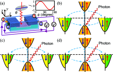
Before discussing the principle of spin-battery, let’s outline PGE from the point of view of photo-excitation, using Fig. 1(b) which describes spin-degenerate case by replacing the FM metal with nonmagnetic metal such as Cu or Au. By absorbing photons, electrons are excited from the valence bands (VB) to the conduction bands (CB), and they flow out of the semiconductor to the left or right. At the same time, the holes left in VB are filled with electrons coming from the two metals. These processes are indicated by the blue dashed lines in Fig. 1(b). When incident light is polarized in parallel (polarization angle ) or perpendicular () to the mirror reflection plane, symmetry is maintained and due to this mirror symmetry, excited electrons have exactly the same probability to flow to the left or right, resulting in zero photocurrent. For other polarization angles , the coupling of polarized photons and electrons in the semiconductor breaks mirror symmetry, hence photo-excited electrons have different probabilities to flow to the left or right, resulting to a net photogalvanic current at zero bias. This PGE current has a distinct dependence on the polarization angle , e.g. varies as for the case of symmetry.
The physical origin of the photocurrent generated by PGE can be understood from the standard phenomenological theoryPGE0 . For a material with Cs symmetry the photocurrent under normal incidence of a linearly polarized light is described by
| (1) |
Here, and are the photocurrents along the directions normal and parallel to the mirror reflection plane, respectively. For the circularly polarized light,
| (2) |
In Eqs.(1) and (2), is the electric field amplitude of the light, , , and are tensors which depend on the photon frequency . Therefore, the PGE is essentially a second-order response to the electric field. Within this scenario, the light illumination contributes to the response coefficients , , and , and thus generates a PGE photocurrent. Therefore, the behavior of the photocurrent either takes a sine or a cosine dependence on the light polarization, determined by both the light and the symmetry of the system.
Having understood the ordinary PGE, we now discuss cases with spins. If magnetic moments of the two FM in the spin-battery are in parallel configuration (PC) as shown in Fig. 1(c), photo-excited electrons - regardless of their spin, act just like that in the nonmagnetic case, because the two spin channels are not coupled (no SOC). Consequently a spin-polarized charge-current is generated by PGE when is not .
Finally, if magnetic moments of the FM are in antiparallel configuration (APC) as shown in Fig. 1(d), the mirror reflection symmetry of the device for individual spin channel is broken by the majority/minority density of states in the FM. Then, both spin-up and -down PGE currents are generated for all angles , including at , and . Note that even though the spin distribution is different in APC as compared to PC, the charge distribution is the same in PC and APC (also nonmagnetic case). Therefore the total charge-current must behave the same way as that in PC and/or in nonmagnetic case, namely must vanish at , and . We therefore arrive at a most interesting conclusion for APC: namely since are nonzero at by PGE but vanishes at these angles, and must be equal in magnitude but flow in exactly opposite direction. In other words, for a device without inversion symmetry but is mirror symmetric, a nonzero spin-current without an accompanying charge-current can be generated by PGE in APC. This device behaves as a spin battery because in open circuit, a spin resolved chemical potential difference is established on the two sides of the device due to the action of PGE. The device in Fig. 1(d) is the pure spin-battery which will be the focus of the rest of the paper.
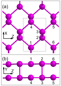
Having qualitatively understood the pure spin-battery, we now implement the idea using the 2D phosphorene as the semiconductor. The phosphorene has a puckered structure with four P atoms in primitive cell as shown in Fig. 2(a). It has a spatial inversion symmetry which belongs to the point group with the inversion center located between the atoms 2 and 3 indicated in Fig. 2(a). This means that the symmetry is invariant when interchanging the atoms 1, 2 and 6 with atoms 5, 3 and 4, respectively. It is essential to break this intrinsic inversion symmetry to have PGE. This is actually not difficult because the local Schottky electric field formed at the metal/phosphorene contacts breaks the inversion symmetry, as shown experimentally (albeit in a different material)Agarwal .
III Model and methods
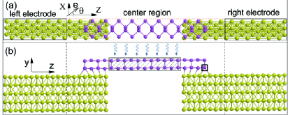
Hence, we construct a FM/semiconductor/FM structure whose energy diagram is that in Fig. 1(c,d) where the FM is nickel (Ni) and the semiconductor is phosphorene, as shown in Fig. 3 (a). Phosphorene has a symmetry in which the zigzag direction is perpendicular to the mirror reflection plane. Again, the formation of Ni/phosphorene interface leads to a Schottky potential that breaks the inversion symmetry of phosphoreneAgarwal . For instance, the electrostatic potential at atom 2 does not equal to that at atom 3, owing to the broken inversion symmetry. Note that the central region of the spin-battery is a composite system of Ni/phophorene/Ni.
The device model consists of three parts including the left- and right-hand nickel electrodes, and the center region, as shown in Fig. 3(a). The electrodes are modeled by a five-layer Ni(111) slabs consisting of atoms in each layer, and the two electrodes extend to , respectively. The left- and right-hand electrodes are the mirror images of each other. In the center region, the phosphorene bridges and partially overlaps the two Ni(111) electrodes, with a vertical Ni-P distance of 2.0 Å determined by the vasp calculationvasp . The whole system periodically extends in the direction with a periodicity of 4.316 Å. The calculated lattice constants of the phosphorene are =3.32 Å, and =4.58 Å which is homogeneously strained by about in order to match the Ni lattice in the direction. The bandgap of the phosphorene is 1.03eV calculated with the local density approximation.
The pristine phosphorene has a spatial inversion symmetry and belongs to point group with a mirror reflection plane (the - plane) perpendicular to the zigzag () direction. However, the contact with the electrodes breaks the symmetry of the pristine phosphorene, which can be easily seen from the side view of the center region shown in Fig. 3(b). Even though, the mirror reflection plane (the - plane) still remains, as can be observed from Fig. 3(a). Thus the phototransistor possesses the symmetry, owing to which we can obtain a spin-polarized photocurrent generated by the PGE.
We have developed a theoretical approach to calculate the photocurrent generated by the PGE based on density functional theory within the nonequilibrium Green’s function (NEGF-DFT) formalismxie and implemented it in the first-principles quantum transport package nanodcalTaylor . Specifically, for the linearly polarized light the photocurrent injecting into the lead L can be written asxie ,
where
For the circularly polarized light, we obtain:
where is same as that in linear polarized case and
In Eqs.(III) and (III), where is the bare electron mass; is the photon flux defined as the number of photons per unit time per unit area; is the frequency and the speed of the light; is the relative magnetic susceptibility, the relative dielectric constant, and the dielectric constant. is the number of photons. In the above expressions, are the retard/advanced Green’s functions without photons, and are the greater/lesser Green’s function without photons. is the cartesian component of the electron momentum, and is the cartesian component of the unit vector e1/2 which characterizes the polarization of the light. For a elliptically polarized light the polarization vector e=e1e2, where “” denotes the right/left handed elliptical light, and determines its helicity. In particular, corresponds to the circularly polarized light. For a linearly polarized light e=e1+e2, where is the angle formed by the polarization direction with respect to the vector . We calculate a normalized photocurrent, i.e. the photoresponse function written as , which still has a dimension of area, i.e., /phonon where is the Bohr radius. We note that for laser power of 0.1 to 105 with an illumination area of 1 , the calculated photocurrent is from 1 to 1 , which can be measured experimentallyacsnano-Wu ; BpOpt2 .
We calculate PGE current along the zigzag () phosphorene direction under linearly or circularly polarized light vertically incident to the phosphorene ( direction), indicated by the wiggly arrows in Fig. 3(b). The light is polarized in the - plane, and for linearly polarized light the polarization vector e forms an angle with respect to the zigzag direction. A wide range of photon energies from 1.2 eV to 2.0 eV are investigated. SOC is not considered to reduce computational cost: we verified that including SOC does not qualitatively change any results. In the NEGF-DFT numerical calculations, double-zeta polarized (DZP) atomic orbital basis was used to expand all the physical quantities; the exchange and correlation were treated at the level of local density approximation; and atomic cores are defined by the standard norm conserving nonlocal pseudopotentials. In the self-consistent calculations and the photocurrent transport calculations of the two-probe device structures (Fig. 3), k-points were used. These calculation details were verified to obtain converged results. Unless otherwise specified, collinear spin is used for the NEGF-DFT calculations in which spin polarizations at different places are all along the same direction in either parallel or anti-parallel configuration.
IV Results and discussion
IV.1 PGE spin-battery
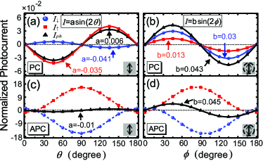
We first consider the case of PC [see Fig. 1(c)] for which the calculated PGE photocurrent versus the polarization angle for linearly polarized light is presented in Fig. 4(a). The PGE photocurrent is spin-polarized and both I↑ and I↓ vary as sin(2) and have opposite sign (i.e. opposite flow direction). Specifically, I↑ (red square) and I↓ (blue sphere) are well fitted as I (red line) and I (blue line), respectively. Consequently, the total PGE charge-current, Iph=I↑ + I↓ (dark triangles) also has a sinusoidal shape (black line) which is a characteristic feature of linear photogalvanic effect (LPGE)PGE0 ; PGE2 . For circularly polarized light, Fig. 4(b) shows that the I↑ and I↓ have the same sign, and both vary in terms of sin(2) where is the helicity of the circularly polarized light. The photocurrents are also well fitted with sine function (lines) as shown in Fig. 4(b). The sine dependence of photocurrent on the helicity of circularly polarized light is the well known circular PGE (CPGE)PGE2 ; PGE3 ; PGE3a ; PGE4 . These numerical results are perfectly consistent with the qualitative discussion above: for instance at , and , I↑, I↓ and Iph all vanish, as we argued above by the PC model of Fig. 1(c).
The variation of the PGE current in terms of sin(2) or sin(2) under linear or circular polarized light, is the typical behavior of PGE determined by the symmetry. According to the phenomenological theory of PGEPGE0 , whether the photocurrent is a sine or a cosine depends on the symmetry. For systems with symmetry, the photocurrent generated in the direction perpendicular to the mirror reflection plane is a sine, which is in perfect agreement with our first-principles results presented here. Note that the phenomenological theory has been widely adopted to explain experimental observations of LPGE and CPGE, for instances for p-GaAs/AlGaAs quantum well systems having symmetryPGE2 .
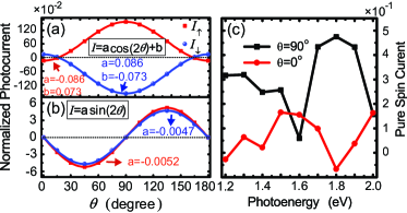
As argued in the qualitative discussion above, the pure spin-battery is established by the device in APC [see Fig. 1(d)] for which the calculated photocurrents by LPGE and CPGE are shown in Figs. 4(c,d), respectively. The total photocurrent (dark triangles) are exactly in a shape of sin(2) for LPGE or sin(2) for CPGE, and are well fitted by the sine function (dark lines). In contrast, for individual spin channels, I↑ and I↓ have opposite sign and appear more like a cosine function. As a result, at , and , the calculated total PGE charge-current Iph is essentially zero, while the spin-current Is=II↓ is nonzero. Namely, the spin-battery generates a pure spin-current without an accompanying charge-current at these polarization angles. The calculated data are in perfect consistency with the qualitative discussion above.
To further understand the origin of pure spin-current generated by spin-battery, we now analyze the photocurrent which, if generated by linearly polarized light, has three components proportional to sin), cos) and sin(), respectively [Eq.(1)]. The first two terms can be expressed in terms of cos(2). In APC (spin-battery), the charge distribution in the device remains to have symmetry, since the anti-parallel spin configuration does not influence the charge distribution as mentioned above. Therefore, Iph should be proportional to sin(). However, spin distribution of the system is no longer mirror-symmetric in APC, therefore the two spin-resolved currents I↑, I↓, should neither be a perfect sine function nor a perfect cosine function. For linearly polarized light, I↑ and I↓ have both cos(2) and sin() components, although the former has a much larger amplitude as shown in Figs. 5(a,b). It is thus concluded that I↑ and I↓ flow in opposite directions with the same magnitude at , and , as the total photocurrent Iph=I↑+ I↓ vanishes due to its sine dependence on . A similar argument holds for circularly polarized light. Therefore, in APC or the spin-battery, PGE generates a pure spin-current at polarization angles , and . These results are what expected from the model presented in Fig. 1(d), and also understandable from the phenomenological point of viewPGE0 .
Our calculation show that the linearly and circularly polarized light generates the same pure spin-current at , also at , which is also expected as at these angles the circularly polarized light has only one polarization vector hence equivalent to a linearly polarized light. Fig. 5(c) plots the calculated operational points of the spin-battery in terms of the photon energy in the range of 1.2 eV to 2.0eV and polarization angle . Namely, at the calculated data points, the spin-battery delivers pure spin-currents without an accompanying charge-current.
The PGE spin-battery is not limited to phosphorene but applicable in general as long as the appropriate symmetry condition is satisfied. For example, substituting the newly reported 2D puckered-arseneneas1 ; as2 ; as3 for the phosphorene should also be able to generate pure spin-current due to a similar structural symmetry. The flow of pure spin-current without an accompanying charge current is usually detected via the inverse spin-Hall effectISH ; opt4 ; ISH1 . For PGE spin-battery, a convenience is the characteristic sinusoidal dependence of the photocurrent which can serve as evidence for successful generation of pure spin-current, namely the PGE spin-battery not only generates pure spin-current but also provides detection by itself. Very interestingly, a recent experiment reported a persistent photocurrent in a few-layer phosphorous at zero source-drain biasBpOpt2 . While the measured data were not interpreted by the PGE physicsPGE0 , the form of the observed photocurrent versus polarization angle suggests that it was likely due to PGE. We conclude that 2D PGE in materials without SOC such as phosphorene to be quite feasible and the PGE spin-battery realizable.
IV.2 PGE spin-battery with disorders and SOC
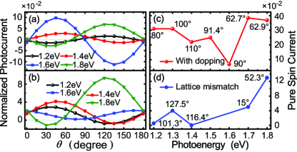
The symmetry property of the spin-battery structure is so far emphasized to interpret results. In reality, an absolutely perfect symmetry (e.g. ) is difficult to achieve due to experimental factors such as the existence of impurities and slight differences in the two Ni/phosphorene contacts. Hence the stability against such perturbations should be examined. Concerning effects of impurity, a recent experiment showed that phosphorene can be alloyed with As atoms up to 80% As concentrationas2 . We thus calculated a system by substituting an As atom for the rightmost P atom in the bottom sub-layer of the phosphorene [See Fig. 3(a)]. Concerning asymmetry in the two Ni/phosphorene contacts, we calculated a system by displacing the right Ni contact and the connected Ni(111) substrate in the central region by 0.2 Å along the direction, corresponding to a mismatch of 4.63% relative to the lattice constant (4.316 Å) of Ni(111) surface in the direction. Both these changes break symmetry of the original ideal spin-battery in Fig. 1 (d) of the main text. The calculated photocurrent becomes that presented in Figs. 6(a,b) and several observations are in order. First, the PGE photocurrent changes from a perfect sin(2) of the ideal spin-battery to a form of sin(2+)+, where and are a phase shift and a constant depending on the photon energy, as shown by different curves in Figs. 6(a,b). Second, compared with results of ideal spin-battery, the photocurrent is not so much affected by the As impurity as shown in Fig. 6(a), but is significantly altered due to the contact asymmetry as shown in Fig. 6(b). Third and most important, although the photocurrent is no longer a perfect sine function on the polarization angle, zero still occurs at certain polarization angles and photon energies, as evidenced in Figs. 6(a,b). In other words, the non-ideal spin-battery still generates pure spin-current even with the structural perturbations. Figs. 6(c,d) present the calculated operation points of the non-ideal spin-battery in terms of the photon energy and polarization angle, this is to be compared with that of Fig. 4 (c) for the ideal spin-battery. We conclude that the spin-battery works whether it is ideal or perturbed, albeit at some different photon energies and polarization angles. Importantly, the signature of pure spin-current generation is when the total photocurrent vanishes which provides the operational point of the device whether it is ideal or not.
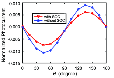
It is interesting to investigate if the SOC effect will significantly alter the outcome of the spin-battery. To this end, we carried out calculations for the same spin-battery system by including SOC in the first principles analysis. Results show that the photocurrent is still a perfect sin(2), as shown in Fig. 7, which qualitatively well agrees with results where SOC is neglected.
In summary, we found that the 2D spin-battery device operated on PGE can deliver a pure spin-current without an accompanying charge-current to the outside world, which is important for 2D flexible spintronics. The device principle is implemented in the 2D material phosphorene and first principles calculations gave numerical data in excellent qualitative agreement with the PGE physics. The PGE spin-battery has excellent operational stability against structural disorder, photon energy and flux, and other material details. The 2D spin-battery is interesting as it is a device that generates pure spin-currents, an energy source that harvest photons, as well as a pure spin-current detector itself. Finally, given the recent experimental discovery of 2D ferromagnetismgong1 ; huang1 , the PGE spin-battery may be entirely realized by layered materials.
Y.W. is grateful to Drs. Lei Liu, Yanxia Xing and Chao-Cheng Kaun for useful discussions. This work was supported by the National Natural Science Foundation of China under grant No. 11404273 and 11774217 (Y.W.) and No. 51871156 (Y.X.), the University Grant Council (Contract No. AoE/P-04/08) of the Government of HKSAR (Y.W., J.W., H.G.).
References
- (1) G. Fiori, F. Bonaccorso, G. Iannaccone, T. Palacios, D. Neumaier, A. Seabaugh, S. K. Banerjee, and L. Colombo, Electronics based on two-dimensional materials, Nat. Nanotechnol. 9, 768 (2014).
- (2) A. Nathan, A. Ahnood, M. T. Cole, S. Lee, Y. Suzuki, P. Hiralal, F. Bonaccorso, T. Hasan, L. Garcia-Gancedo, A. Dyadyusha, S. Haque, P. Andrew, S. Hofmann, J. Moultrie, D. Chu, A. J. Flewitt, M. J. Ferrari, A C abd Kelly, J. Robertson, G. A. J. Amaratunga, and W. I. Milne, Flexible electronics: The next ubiquitous platform., Proc. IEEE 100, 1486 (2012).
- (3) S. A. Wolf, D. D. Awschalom, R. A. Buhrman, J. M. Daughton, S. von Molnar, M. L. Roukes, A. Y. Chtchelkanova, and D. M. Treger, Spintronics: a spin-based electronics vision for the future, Science 294, 1488 (2001).
- (4) I. Zutic, J. Fabian, and S. D. Sarma, Spintronics: Fundamentals and applications , Rev. Mod. Phys. 76, 323 (2004).
- (5) M. Harder, Y. Gui, and C.-M. Hu, Electrical detection of magnetization dynamics via spin rectification effects, Phys. Rep. 661, 1 (2016).
- (6) V. I. Belinicher and B. I. Sturman, The photogalvanic effect in media lacking a center of symmetry, Sov. Phys. Usp. 23, 199 (1980).
- (7) S. Dhara, E. J. Mele, and R. Agarwal, Voltage-tunable circular photogalvanic effect in silicon nanowires, Science 349, 726 (2015).
- (8) P. Olbrich, S. A. Tarasenko, C. Reitmaier, J. Karch, D. Plohmann, Z. D. Kvon, and S. D. Ganichev, Observation of the orbital circular photogalvanic effect, Phys. Rev. B 79, 121302 (2009).
- (9) J. Karch, S. A. Tarasenko, E. L. Ivchenko, J. Kamann, P. Olbrich, M. Utz, Z. D. Kvon, and S. D. Ganichev, Photoexcitation of valley-orbit currents in (111)-oriented silicon metal-oxide-semiconductor field-effect transistors, Phys. Rev. B 83, 121312 (2011).
- (10) S. D. Ganichev, E. L. Ivchenko, V. V. Bel’kov, S. A. Tarasenko, M. Sollinger, D. Weiss, W. Wegscheider, and W. Prettl, Spin-galvanic effect, Nature 417, 153 (2002).
- (11) S. D. Ganichev, H. Ketterl, W. Prettl, E. L. Ivchenko, and L. E. Vorobjev, Circular photogalvanic effect induced by monopolar spin orientation in p-GaAs/AlGaAs multiple-quantum wells, Appl. Phys. Lett. 77, 3146 (2000).
- (12) S. D. Ganichev, E. L. Ivchenko, S. N. Danilov, J. Eroms, W. Wegscheider, D. Weiss, and W. Prettl, Conversion of spin into directed electric current in quantum wells, Phys. Rev. Lett. 86, 4358 (2001).
- (13) S. D. Ganichev and W. Prettl, Spin photocurrents in quantum wells, J. Phys.: Condens. Matter 15, R935 (2003).
- (14) C. Yin, H. Yuan, X. Wang, S. Liu, S. Zhang, N. Tang, F. Xu, Z. Chen, H. Shimotani, Y. Iwasa, Y. Chen, W. Ge, and B. Shen, Tunable surface electron spin splitting with electric double-layer transistors based on InN, Nano Lett. 13, 2024 (2013).
- (15) H. Yuan, X. Wang, B. Lian, H. Zhang, X. Fang, B. Shen, G. Xu, Y. Xu, S.-C. Zhang, H. Y. Hwang, and Y. Cui, Generation and electric control of spin-valley-coupled circular photogalvanic current in WSe2, Nat. Nanotechnol. 9, 851 (2014).
- (16) M. Eginligil, B. Cao, Z. Wang, X. Shen, C. Cong, J. Shang, C. Soci, and T. Yu, Dichroic spin-valley photocurrent in monolayer molybdenum disulphide, Nat. Commun. 6, 7636 (2015).
- (17) C. Kastl, C. Karnetzky, H. Karl, and A. W. Holleitner, Ultrafast helicity control of surface currents in topological insulators with near-unity fidelity, Nat. Commun. 6, 6617 (2015).
- (18) K. N. Okada, N. Ogawa, R. Yoshimi, A. Tsukazaki, K. S. Takahashi, M. Kawasaki, and Y. Tokura, Enhanced photogalvanic current in topological insulators via Fermi energy tuning , Phys. Rev. B 93, 081403 (2016).
- (19) J. W. McIver, D. Hsieh, H. Steinberg, P. Jarillo-Herrero, and N. Gedik, Control over topological insulator photocurrents with light polarization , Nat. Nanotechnol. 7, 96 (2012).
- (20) G. E. W. Bauer, E. Saitoh, and B. J. van Wees, Spin caloritronics, Nat. Mater. 11, 391 (2012).
- (21) J. Tian, S. Hong, I. Miotkowski, S. Datta, and Y. P. Chen, Observation of current-induced, long-lived persistent spin polarization in a topological insulator: A rechargeable spin battery, Sci. Adv. 3, e1602531 (2017).
- (22) J. E. Hirsch, Spin Hall Effect, Phys. Rev. Lett. 83, 1834 (1999).
- (23) D. Ellsworth, L. Lu, J. Lan, H. Chang, P. Li, Z. Wang, J. Hu, B. Johnson, Y. Bian, J. Xiao, R. Wu, and M. Wu, Photo-spin-voltaic effect, Nat. Phys. 12, 861 (2016).
- (24) Y. Kajiwara, K. Harii, S. Takahashi, J. Ohe, K. Uchida, M. Mizuguchi, H. Umezawa, H. Kawai, K. Ando, K. Takanashi, S. Maekawa, and E. Saitoh, Transmission of electrical signals by spin-wave interconversion in a magnetic insulator, Nature 464, 262 (2010).
- (25) S. W. Jiang, S. Liu, P. Wang, Z. Z. Luan, X. D. Tao, H. F. Ding, and D. Wu, Exchange-dominated pure spin current transport in molecules, Phys. Rev. Lett. 115, 086601 (2015).
- (26) J. B. S. Mendes, O. Alves Santos, L. M. Meireles, R. G. Lacerda, L. H. Vilela-Leão, F. L. A. Machado, R. L. Rodríguez-Suárez, A. Azevedo, and S. M. Rezende, Spin-current to charge-current conversion and magnetoresistance in a hybrid structure of graphene and yttrium iron garnet, Phys. Rev. Lett. 115, 226601 (2015).
- (27) K. Uchida, S. Takahashi, K. Harii, J. Ieda, W. Koshibae, K. Ando, S. Maekawa, and E. Saitoh, Observation of the spin Seebeck effect, Nature, 455, 778 (2008).
- (28) D. Meier, T. Kuschel, L. Shen, A. Gupta, T. Kikkawa, K. Uchida, E. Saitoh, J.-M. Schmalhorst, and G. Reiss, Thermally driven spin and charge currents in thin NiFe2O4/Pt films, Phys. Rev. B 87, 054421 (2013).
- (29) P. Li, D. Ellsworth, H. Chang, P. Janantha, D. Richardson, F. Shah, P. Phillips, T. Vijayasarathy, and M. Wu, Generation of pure spin currents via spin seebeck effect in self-biased hexagonal ferrite thin films, Appl. Phys. Lett. 105, 242412 (2014).
- (30) W. Lin, K. Chen, S. Zhang, and C. L. Chien, Enhancement of thermally injected spin current through an antiferromagnetic insulator, Phys. Rev. Lett. 116, 186601 (2016).
- (31) J. F. Sierra, I. Neumann, J. Cuppens, B. Raes, M. V. Costache, and S. O. Valenzuela, Thermoelectric spin voltage in graphene, Nat. Nanotechnol. 13, 107 (2018).
- (32) L. Berger, Generation of dc voltages by a magnetic multilayer undergoing ferromagnetic resonance, Phys. Rev. B 59, 11465 (1999).
- (33) G. Schmidt, D. Ferrand, L. W. Molenkamp, A. T. Filip, and B. J. van Wees, Fundamental obstacle for electrical spin injection from a ferromagnetic metal into a diffusive semiconductor, Phys. Rev. B 62, R4790 (2000).
- (34) E. I. Rashba, Theory of electrical spin injection: Tunnel contacts as a solution of the conductivity mismatch problem, Phys. Rev. B 62, R16267 (2000).
- (35) A. Brataas, Y. Tserkovnyak, G. E. W. Bauer, and B. I. Halperin, Spin battery operated by ferromagnetic resonance, Phys. Rev. B 66, 060404(R) (2002).
- (36) L. Li, Y. Yu, G. J. Ye, Q. Ge, X. Ou, H. Wu, D. Feng, X. H. Chen, and Y. Zhang, Black phosphorus field-effect transistors, Nat. Nanotechnol. 9, 372 (2014).
- (37) J. Qiao, X. Kong, Z.-X. Hu, F. Yang, and W. Ji, High-mobility transport anisotropy and linear dichroism in few-layer black phosphorus, Nat. Commun. 5, 4475 (2014).
- (38) V. Tran, R. Soklaski, Y. Liang, and L. Yang, Layer-controlled band gap and anisotropic excitons in few-layer black phosphorus, Phys. Rev. B 89, 235319 (2014).
- (39) M. Buscema, D. J. Groenendijk, G. A. Steele, H. S. J. van der Zant, and A. Castellanos-Gomez, Photovoltaic effect in few-layer black phosphorus PN junctions defined by local electrostatic gating, Nat. Commun. 5, 4651 (2014).
- (40) M. Buscema, D. J. Groenendijk, S. I. Blanter, G. A. Steele, H. S. J. van der Zant, and A. Castellanos-Gomez, Fast and broadband photoresponse of few-layer black phosphorus field-effect transistors, Nano Lett. 14, 3347 (2014).
- (41) T. Hong, B. Chamlagain, W. Lin, H.-J. Chuang, M. Pan, Z. Zhou, and Y.-Q. Xu, Polarized photocurrent response in black phosphorus field-effect transistors, Nanoscale 6, 8978 (2014).
- (42) Q. Guo, A. Pospischil, M. Bhuiyan, H. Jiang, H. Tian, D. Farmer, B. Deng, C. Li, S.-J. Han, H. Wang, Q. Xia, T.-P. Ma, T. Mueller, and F. Xia, Black phosphorus mid-infrared photodetectors with high gain, Nano Lett. 16,4648 (2016).
- (43) M. V. Kamalakar, B. N. Madhushankar, A. Dankert, and S. P. Dash, Low Schottky barrier black phosphorus field-effect devices with ferromagnetic tunnel contacts, Small 11, 2209 (2015).
- (44) M. Huang, M. Wang, C. Chen, Z. Ma, X. Li, J. Han, and Y. Wu, Broadband black-phosphorus photodetectors with high responsivity, Adv. Mater. 28, 3481 (2016).
- (45) G. Kresse and J. Furthmüller, Efficient iterative schemes for ab initio total-energy calculations using a plane-wave basis set, Phys. Rev. B 54, 11169 (1996).
- (46) Y. Xie, L. Zhang, Y. Zhu, L. Liu, and H. Guo, Photogalvanic effect in monolayer black phosphorus, Nanotechnology 26, 455202 (2015).
- (47) J. Taylor, H. Guo, and J. Wang, Ab initio modeling of quantum transport properties of molecular electronic devices, Phys. Rev. B 63, 245407 (2001).
- (48) J. Wu, G. K. W. Koon, D. Xiang, C. Han, C. T. Toh, E. S. Kulkarni, I. Verzhbitskiy, A. Carvalho, A. S. Rodin, S. P. Koenig, G. Eda, W. Chen, A. H. C. Neto, and B. Ozyilmaz, Colossal ultraviolet photoresponsivity of few-layer black phosphorus, ACS Nano 9, 8070 (2015).
- (49) C. Kamal and M. Ezawa, Arsenene: Two-dimensional buckled and puckered honeycomb arsenic systems, Phys. Rev. B 91, 085423 (2015).
- (50) B. Liu, M. Kopf, A. N. Abbas, X. Wang, Q. Guo, Y. Jia, F. Xia, R. Weihrich, F. Bachhuber, F. Pielnhofer, H. Wang, R. Dhall, S. B. Cronin, M. Ge, X. Fang, T. Nilges, and C. Zhou, Black arsenic phosphorus: layered anisotropic infrared semiconductors with highly tunable compositions and properties, Adv. Mater. 27, 4423 (2015).
- (51) Z. Zhu, J. Guan, and D. Tománek, Structural transition in layered As1-xPx compounds: a computational study, Nano Lett. 15, 6042 (2015).
- (52) S. O. Valenzuela and M. Tinkham, Direct electronic measurement of the spin Hall effect , Nature 442, 176 (2006).
- (53) D. Sun, J. v. Schootech, M. Kavand, H. Malissa, C. Zhang, M. Groesbeck, C. Boehme, and Z. V. Vardeny, Inverse spin Hall effect from pulsed spin current in organic semiconductors with tunable spin-orbit coupling, Nat. Mater. 15, 863 (2016).
- (54) C. Gong, L. Li, Z. Li, H. Ji, A. Stern, Y. Xia, T. Cao, W. Bao, C. Wang, Y. Wang, Z. Q. Qiu, R. J. Cava, S. G. Louie, J. Xia, and X. Zhang, Discovery of intrinsic ferromagnetism in two-dimensional van der waals crystals, Nature 546, 265 (2017).
- (55) B. Huang, G. Clark, E. Navarro-Moratalla, D. R. Klein, R. Cheng, K. L. Seyler, D. Zhong, E. Schmidgall, M. A. McGuire, D. H. Cobden, W. Yao, D. Xiao, P. Jarillo-Herrero, and X. Xu, Layer-dependent ferromagnetism in a van der waals crystal down to the monolayer limit, Nature 546, 270 (2017).