Modeling Transient Negative Capacitance in Steep-Slope FeFETs
Abstract
We report on measurements and modeling of FE HfZrO/SiO2 Ferroelectric-Dielectric (FE-DE) FETs which indicate that many of the phenomena attributed to Negative Capacitance can be explained by a delayed response of ferroelectric domain switching - referred to as Transient Negative Capacitance (TNC). No traversal of the stabilized negative capacitance branch is required. Modeling is used to correlate the hysteretic properties of the ferroelectric material to the measured transient and subthreshold slope (SS) behavior. It is found that steep SS can be understood as a transient phenomenon, present when significant polarization changes occur. The experimental signature of TNC is investigated, and guidelines for detecting it in measured data are outlined. The technological implications of FE polarization switching are investigated, and it is found that NCFETs relying on it are not suitable for high performance CMOS logic, due to voltage, frequency, and hysteresis limitations. Requirements for experimental evidence of stabilized S-curve behavior are summarized.
Index Terms:
Ferroelectric, FeCap, Negative Capacitance, NCFET, FeFETI Introduction
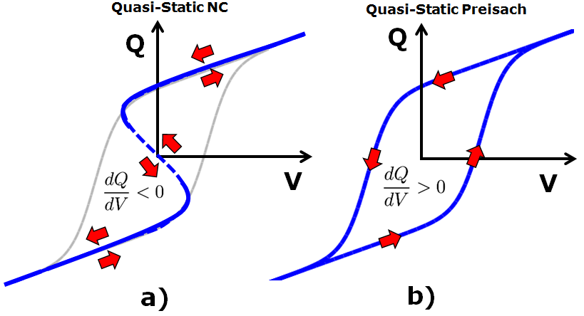
Negative capacitance has been postulated theoretically [1] and extensively studied experimentally ([2], [4], [5]). The theoretical basis for Negative Capacitance (NC) is an assumed Energy-Charge (U-Q) relationship with a region of negative curvature (U-Q ansatz) [1]. As a consequence of the negative curvature, a switching path with negative capacitance (Fig. 1a) becomes available. This is in contrast to the standard Preisach model of a ferroelectric capacitor (Fig. 1b). However, this path is unstable and not directly observable in stand-alone FeCaps. Arguments have been made [1] that this unstable path can be stabilized by connecting the FeCap in series with a standard (positive U-Q curvature) capacitor which satisfies specific matching criteria [9], thereby making the negative capacitance branch traversable. As a consequence, using such a capacitor arrangement in the gate stack of a FET would result in increased stack capacitance and sub-60 mV/dec subthreshold slope ([1], [2]). However, precisely how the stabilized state is established at the microscopic level is unclear at the present, and challenging to explain. In the face of this difficulty, the goal of this paper is to investigate whether some of the key experimental findings, including sub-60 mV/dec SS, can in fact be reproduced without the U-Q ansatz, consequently doing away with the need for a microscopic model of the stabilized state. In this work, which is an extended version of [3] (adding additional explanatory material), the alternative conceptual model proposed is simply a Preisach Ferroelectric ([10], [11]) with slow ferroelectric (FE) switching dynamics. The presence of slow switching dynamics of ferroelectric domains is itself well known and characterized, with little ambiguity with regards to the microscopic model ([13], [14], [15]).
II Modeling and Pulse-Based Verification
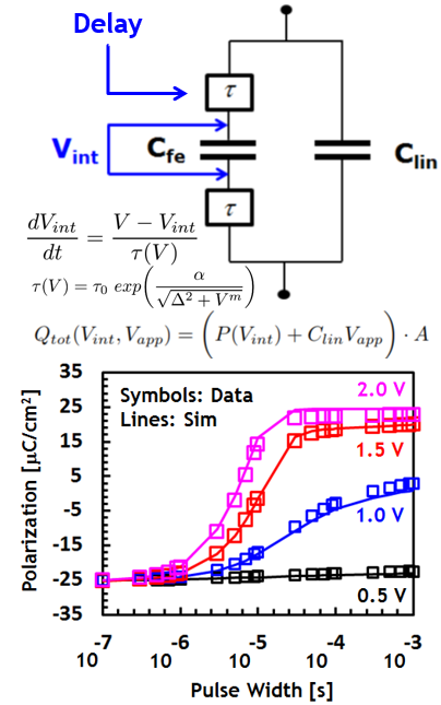
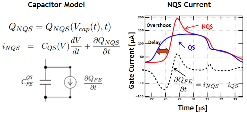
The overall model for the FeCap consists of two components: a delayed ferroelectric polarization capacitance, and a quasistatic non-ferroelectric capacitance. The ferroelectric response is delayed due to the intrinsic switching dynamics of the Fe domains, while the non-ferroelectric component is governed by fast electronic polarization. The ferroelectric response is modeled as a quasistatic Preisach FeCap combined with an explicit delay, using a dynamic turning-point model to describe the hysteresis (Fig. 2, top). In this work, the delay is assumed to be due to the internal switching dynamics of ferroelectric domains, but no attempt is made to explain the detailed microscopic origin [15]. The quasistatic parameters of the FeCap model are calibrated using the data of [5], as shown in Fig. 2. In this work, (Fig. 2) is governed by a first-order delay of the applied voltage across the FeCap, using a form of Merz’s Law. (Fig. 2, inset). The free charge on the capacitor plates is assumed to be quasi-static w.r.t. the total polarization (valid for continuum model and normal CMOS operation).
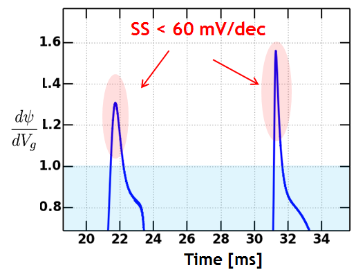
The applicability of the model is tested by comparing predictions to pulse-train data of [5]. For bipolar switching, the square waveform ranges from -VDD to +VDD, exercising both the positive and negative domain switching thresholds. Both the measured data and simulation (Fig. 3) exhibit an initial voltage spike, followed by a more gradual rise to the peak pulse voltage. Arguing from the standpoint of a delayed ferroelectric response, the “spike” behavior can be understood as follows. The voltage across the stack initially rises quickly, with only the non-ferroelectric polarization responding. A s or so later, the ferroelectric domains begin to switch, and the polarization increases dramatically. This is balanced by by an increase in current, which in turn drops more voltage across the access resistor, resulting in a brief drop in the voltage across the stack. The voltage then gradually rises as additional ferroelectric domains switch and the capacitors absorbs more charge. The P-V trajectory (Fig. 3, right) shows regions of Transient Negative Capacitance (TNC) where the voltage across the stack is decreasing.
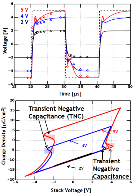
Additional insight into the switching behavior is gained by examining the VDD behavior of the switching in Fig. 3. It is apparent that the “spike” effect is diminishing with decreasing pulse amplitude. While quite pronounced at 5V, it is completely absent at 2V (data and model). The reason is that at low pulse voltages the voltage drop across the FeCap is too small to trigger ferroelectric domains. From Fig. 2, it is evident that very little ferroelectric switching happens in the voltage range of [-1.5V, 1.5V], which is the approximate voltage range across the FeCap during the 2V pulse. In the Verilog-A model, the delay is associated only with ferroelectric switching, so absent switching, there is negligible delay (and hence no spike).
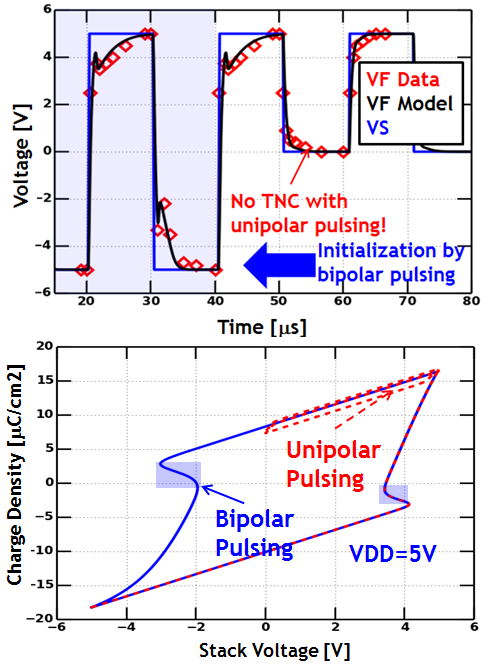
For unipolar switching, the square input waveform is modified to range from 0 to VDD. The results are qualitatively different than for the bipolar case. As can be seen in Fig. 4, the “spike” is observed only on the first unipolar pulse of the waveform. Subsequent pulses exhibit no spike at any voltage. This behavior is reproduced in simulation. The reason for the behavior of the stack voltage is apparent from Fig. 4 (bottom) . While the polarization undergoes large changes during bipolar switching, the only large polarization change during unipolar switching is during the transition from bipolar to unipolar mode. After this initial pulse, the FeCap operates on a tight minor loop, and the polarization changes are small and mostly due to non-ferroelectric polarization. As previously discussed, non-ferroelectric polarization is essentially quasistatic, so there is a negligible amount of delayed polarization. Hence, no spike is produced.
III Impact on Subthreshold Slope
The technological impetus for investigating the NC-effect is the potential improvement in FET subthreshold slope (SS). As argued in [1], a negative capacitance gate layer can result in a sub-60 mV/dec SS, by introducing “amplification” into the surface potential (). Specifically, if the applied gate bias is Vg, the long channel slope of the Id-Vg curve is proportional to . With ordinary capacitors, this derivative is never greater than unity (equal to unity only for long-channel, fully-depleted devices). As shown in [1], NC effects can push the derivative beyond unity, thereby reducing the SS below the usual theoretical limit.
III-A Conceptual Model
In order to gain insight into the effect of the non Quasi-Static TNC behavior of FeCaps, a simple conceptual model is considered first. The charge on the FeCap is a non Quasi-Static (NQS) function of voltage and time, having an explicit temporal dependence due to internal polarization dynamics. In terms of a circuit element description, the NQS FeCap must therefore be modeled as shown in Fig. 5 (left). The form of the NQS current component in the circuit model of Fig. 5 is governed by the polarization dynamics of the FeCap and depends on the details of the model used. Using the previously described model, the current response to a voltage ramp is shown in Fig. 5 (right).
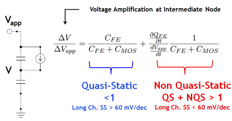
The application of the circuit model for the FeCap of Fig. 5 to a simple capacitive voltage divider is shown in Fig. 6. The voltage at the intermediate node in Fig. 6 is then obtained as:
| (1) | |||
| (2) |
It should be noted that all the and terms in the above equations are functions of the instantaneous voltages across the corresponding capacitors (but not explicitly functions of time; this is handled by the NQS current term ), and are not considered to be constant.
Dividing through by the derivative terms and approximating increments using , one obtains:
| (4) |
Since Eqn. 4 relates the incremental change of the intermediate node potential w.r.t. an incremental change of the applied voltage, it is the sought-after amplification. Under quasi-static conditions (i.e. all NQS currents are very small because the internal dynamics of the FE cap can track a slow voltage ramp) the 2nd term in Eqn. 4 vanishes (i.e. ). In this case, the amplification is always less than unity, approaching unity in the limit of . This is the “normal” MOS regime, in which SS 60 mV/dec. It should be noted that this result holds for arbitrary non-linear capacitive behavior of and ; the only requirement for “normal” MOS behavior is the quasi-static condition. With non quasi-static conditions, however, the 2nd term must be taken into account, as highlighted in Fig. 6 . For cases where is positive (and assuming that is positive), amplification is increased. It should also be noted that the mere presence of the NQS term in Eqn. 4 and Fig. 6 does not guarantee that amplification exceeds unity. Only if the 2nd term is sufficiently large and positive can amplification exceed unity. If this is the case, SS may be less than 60 mV per decade. The key is the behavior of the NQS current, given by . Clearly, extreme simplification assumptions were made in obtaining this result w.r.t. the MOS model: it was treated as a single, lumped capacitance. In reality, it is the surface potential hidden inside this lumped model that is of interest, not just the potential of the intermediate node of Fig. 6. Two and three-dimensional effects were ignored. The details of the FET model are discussed next.
III-B FET Simulation
While the conceptual model is helpful in arguing for the possibility of amplification and sub-60 mV/dec FET behavior, a more detailed accounting of the FET behavior requires simulation with an appropriate FeCap and FET model. The capacitive divider representing the full stack of the FET is illustrated in Fig. 7.
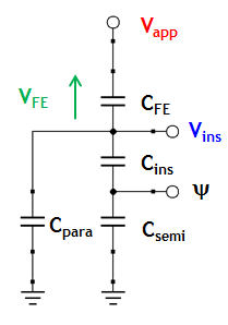
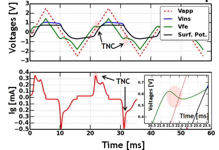
The behavior of the full FET with an applied triangular-wave voltage waveform is simulated using the FeCap model of Sec. II with HSPICE. The resulting waveforms are illustrated in Fig. 8. Regions of TNC are clearly evident: the voltage across the FeCap (green curve) exhibits brief “counter-trend” behavior, in which the voltage drops (rises) during periods when the applied gate voltage rises (drops). This is the same behavior as previously noted in Fig. 3. The reduction in magnitude of the FeCap voltage implies that the potential at the linear capacitor node must be increasing faster than the applied voltage. Viewed from the context of the conceptual model of Sec.III-A, there is a burst of current arising from the delayed FE polarization which rapidly charges the capacitors below the FeCap, increasing the potential at all floating nodes of Fig. 7. This potential increase results in a reduction of voltage across the FeCap while its charge is increasing, i.e. TNC. Thus, in this view, TNC is seen as a side effect of amplification, not its cause.
The values for amplification can be obtained directly from Fig. 7, and are illustrated in Fig. 9. Regions where may correspond to regions where mV/dec for long-channel FETs.
The reason that does not guarantee sub-60 SS long-channel behavior is due to the fact that regions of may not be aligned with sub-threshold values of the surface potential , i.e. the of the FET is not properly selected. This is in fact seen in the current example, as shown in Fig. 10.
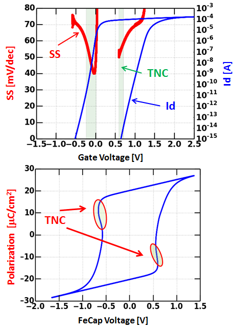
III-C Hysteresis
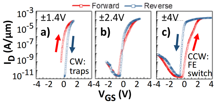
As seen in Fig. 10, sub-60 mV/dec SS is accompanied by significant Id-Vg hysteresis. This is an inescapable result in the presence of polarization switching, resulting in an effective Vt-shift of the underlying FET. Virtually all published measurements of sub-60 mV/dec FETs show this strong correlation of SS improvement and Id-Vg hysteresis. Some reported works do indeed report hysteresis-free sub-60 mV/dec behavior, but a closer inspection reveals the behavior to be only approximately hysteresis-free. Measurements indicate that this is caused by a balance of trap-induced, clockwise hysteresis, and FE switching-induced counter-clockwise hysteresis. This effect is illustrated in Fig. 11.
III-D Frequency and Peak Voltage Dependence
The conceptual model of Sec. III-A suggests that the magnitude of voltage amplification depends on the NQS current. Since the proposed NQS current mechanism is simply a delayed polarization current, it is clear that SS should depend on the amount of switched polarization. Correspondingly, the SS behavior of the NCFET depends on the peak switching voltage (since the latter controls the amount of switched polarization ), but also on the rate at which the applied voltage across the NCFET changes, since the polarization dynamics can only keep up with applied voltage ramps that are not much faster than the polarization delay time. The dependence of the min SS of a single NCFET across a range of peak voltages is shown in Fig. 12.
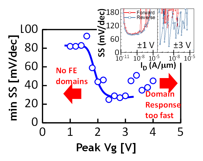
The measured min SS vs. peak Vg follows a “U-shaped” curve, due to two competing effects. At low peak voltages, the voltage across the FeCap stays below the coercive voltage Vc, thereby limiting FE domain switching, resulting in minimal (or no) , and a correspondingly negligible of Eqn. 4. Under such circumstances, SS is expected to be 60 mV/dec, and indeed measured data confirms this. As the peak voltage is increased, the min SS is seen to dip below 60 mV/dec, to as low as 30 mV/dec. In this regime, the voltage across the FeCap does exceed Vc, and large values of and are possible. Finally, further increases in the peak voltage show a gradually increasing min SS. In this regime, there is little or no further increase in the switched FE polarization (peak voltage in the FeCap far exceeds Vc). However, the higher field in the FeCap does result in faster domain switching. This increased switching rate with a fixed input waveform at the gate results in nearly Quasi-Static behavior of the FeCap, reducing the current overshoot in Fig. 5 and the corresponding NQS term in Eqn. 4.
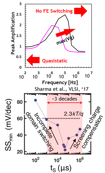
In general, it should be expected that the sub-60 SS behavior (or conversely, surface potential amplification) should be strongly frequency dependent, as illustrated in Fig. 13. The top plot of Fig. 13 shows the simulated amplification factor for a single NCFET, as a function of the frequency of the applied triangular waveform. There is a clear peak, with the amplification decaying at high frequencies (where domain switching is too slow), but also at very low frequencies, where the ferroelectric behavior is quasi-static (as discussed in the context of the peak-Vg dependence). The position of the peak is Vg-dependent, due to the Vg dependence of the FE domain switching speed. The simulated width of the amplification peak spans about two decades in frequency. This behavior is qualitatively reproduced in measured data, as shown in the bottom plot of Fig. 13. The measured min SS is seen to be strongly frequency-dependent (the x-axis parameter is the voltage step time during the triangular ramp, serving here as a proxy for the inverse of the sweep frequency). It should be noted that the bandwidth of the measured sub-60 response is somewhat wider than that of the simulation, spanning about three decades (as compared to about two for simulation). This suggests that the modeled polarization dynamics are not capturing the full complexity of the FE behavior. One obvious modeling simplification is the notion that all the FE domains follow the same switching dynamics. There is no reason for this, and it is not unreasonable to expect that domains with different threshold voltages will likewise have different switching dynamics. This is in fact evident in the measurements of [15], which indicate that there is roughly one order of magnitude spread in switching times of various domains at the same applied voltage. This is one of several indications that treating the FeCap as a continuum is an oversimplification, and that explicitly accounting for domain discreteness is necessary.
III-E Effect of Domain Discreteness
As mentioned in the previous section, treating the FE layer as a continuum is a great model simplification. In fact, HfZrO (and PZT) layers are granular, with a relatively small number of discrete ferroelectric domains. Polarization of the FE layer cannot change in a continuous fashion; it naturally occurs only in discrete jumps. Thus, it should not be surprising that measurements of SS frequently show “noisy” behavior that appears to be consistent with discrete domain switching. An example is shown in the inset of Fig. 12, in which it can be seen that SS has a large random component under conditions in which sub-60 behavior is observed. This random component is not easily dismissed as measurement noise of low-level currents; the same current levels give rise to nearly noise-free SS under conditions in which SS 60 mV/dec (Fig. 12, inset: low peak-Vg values in which no FE switching occurs have SS 60 mV/dec and small noise; high peak-Vg measurements result in sub-60 mV/dec, accompanied by significant SS noise). Additionally, the relatively large average grain size suggests that only a small number of FE domains can be present on a scaled FET. A typical finFET might have a gate area of approximately 3000 (two fins); this would suggest an expectation value of fewer than 10-20 FE domains per FET. Not only is the number of FE domains expected to vary from FET to FET, but their size and threshold voltages as well. Thus, examining a statistical, multi-domain FeCap model is necessary. Following the Preisach [10] approach of treating FeCaps as collections of independent FE domains, a multi-domain can be simply constructed as a parallel combination of a number of individual “hysterons,” where the hysterons are represented by the ideal box-like P-V hysteresis relations. While the full impact of statistical variations is a subject worthy of further investigation, a case of specific interest is illustrated herein. The grain size distribution of [15] suggests that FeCaps consisting of a large domain and a collection of small domains are not unlikely. It is of particular interest then to see the electrical impact of switching a large domain. This is modeled (for example) by an FeCap in which 25% of the area is occupied by a single domain (a hysteron), while the remaining 75% consists of a large number of small domains. The collection of small domains is treated as comprising a continuum, rather than consisting of individual domains (this is done to highlight the effect of the single large domain).
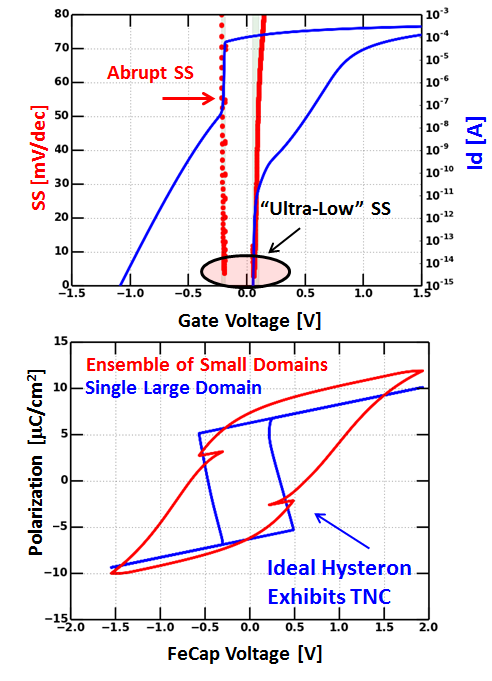
It is clear from Fig. 14 that the presence of the large domain has a significant impact on the Id-Vg characteristics of the FET. Specifically, switching of the large domain produces a very strong TNC effect, resulting in a near-abrupt change in channel current (SS 5 mV/dec). Had this large domain be subdivided into many smaller domains, the resulting current overshoot would have been distributed over many events, producing a more continuous, albeit much less dramatic drop in SS. Numerical experiments suggest that SS values much below 30 mV/dec are not achievable using the continuous model: large discrete domains appear to be necessary. The highly abrupt nature of the SS improvement seen in Fig. 14 is commonly observed in measurements. In fact, most measurements show discrete jumps in SS, rather than continuous sub-60 behavior, but only some demonstrate exceedingly low SS values, such as those of Fig. 14. It is suggested here that these measurements correspond to FETs with a small number of large FE domains.
IV Distinguishing TNC from Stabilized S-Curve
Given the dramatic differences in CMOS applicability of FETs operating on a stabilized S-curve vs. those operating by FE switching, it is important to be able to clearly identify which type of sub-60 SS behavior is manifesting in a given experiment. A simple set of distinguishing conditions is shown in Table I.
| Conditions | TNC | S-Curve | Experiment To Date |
|---|---|---|---|
| Peak VFE VC | No | Yes | No |
| Peak VFE VC | Yes | Yes/No | Yes |
| f fFE | Yes | Yes | Yes |
| f fFE | No | Yes | No |
| Discrete Jumps | Yes | No | Yes |
| Hysteresis | Yes | No | Yes |
In Table I, VFE is the peak voltage across the FE capacitor, VC is the coercive voltage, f is the sweep frequency, and fFE is the response frequency of the FE layer. In order to unequivocally demonstrate S-curve behavior, the FET should demonstrate sub-60 mV/dec SS in the absence of FE switching. As shown in Table I, this requires sub-60 operation at low applied peak voltages (Peak VFE VC), at sufficiently high switching frequencies (f fFE), and with no hysteresis. The voltage and hysteresis criteria are relatively straightforward to apply in measurements; the value of VC can be obtained from the P-V characteristics of the FE layer, and the peak voltage can be kept well below that value.
V Conclusion and Future Direction
A theoretical model of NCFETs which explains sub-60 mV/dec SS as a consequence of slow FE polarization switching has been proposed. The predictions of the model are in qualitative or even quantitative agreement with several classes of measured data. The measured data includes transient pulses across FE-DE stacks for various voltages and polarities, as well as measurements of NCFET SS across a wide range of voltage and sweep rate conditions. The key feature of the model is that the relatively slow FE domain switching dynamics result in NQS behavior of the FE layer. It was shown analytically that gate stacks with NQS components can exhibit voltage amplification, or equivalently, improved SS. The delay in the FE polarization response relative to the applied gate voltage produces NQS bursts of gate current, which can result in sub-60 SS. No explicit negative capacitance is required for this enhancement to take place. In fact, the quasi-static FE capacitance is shown to always be positive, even though voltage amplification in the gate stack implies a transient form of negative capacitance. It was also argued that the transient nature of this enhancement results in significant limitations w.r.t. the application of NCFETs to CMOS logic. Specifically, the FE polarization response time of HZO-based dielectric films is limited to the order of s or slower, rendering sub-60 SS behavior at CMOS circuit speeds impossible. Furthermore, large applied voltages are generally required to produces sub-60 SS behavior; in order for FE domains to switch, the voltage across the FE layer must be comparable to the coercive voltage. For thin films (5nm or less), the coercive voltages are approximately 0.5V. Given the voltage division between the FE and DE layers, applied gate voltages significantly in excess of 1V are required for sub-60 SS, even for thin-film NCFETs.
It was furthermore shown that the discrete domain nature of FE films is responsible for the nearly abrupt jumps in drain current observed in some measured data. Individual domain switching events of large area domains result in large and sudden changes in polarization, leading to nearly abrupt changes in the drain current. NCFETs which contain a small number of large domains can manifest sub-60 SS even at very low sweep rates (i.e. nearly quasi-static), but still not at frequencies exceeded the response frequency of domain switching.
While the NQS model of NCFETs presented in this paper is in good agreement with observed FET behavior to date, this does not necessarily imply that sub-60 mV/dec SS is possible only by relying on delayed polarization switching. The desired NCFET based on the stabilized S-curve may be independently achievable. However, it is important to distinguish polarization switching NCFETs from stabilized S-curve NCFETs when analyzing measured data. For this purpose, a set of guidelines has been presented, suggesting how to distinguish transient NC from the desired stabilized S-curve. Specifically, in order to be confident in the S-curve interpretation of a measured sub-60 mV/dec SS, the experiment must prevent any possibility of FE domain switching. This includes operating at low voltages (well below the coercive voltage of the FE layer) and at frequencies much higher than the response frequency of the FE domains. If sub-60 mV/dec SS is indeed observed under conditions which preclude FE switching, it will be possible to claim that stabilized S-curve operation has in fact been achieved.
References
- [1] S. Salahuddin, S. Datta ”Use of Negative Capacitance to Provide Voltage Amplification for Low Power Nanoscale Devices” Nano Lett., 2008, 8 (2), pp 405-410 DOI: 10.1021/nl071804g.
- [2] A. I. Khan, K. Chatterjee, B. Wang, S. Drapcho, L. You, C. Serrao, S. R. Bakaul, R. Ramesh, S. Salahuddin “Negative capacitance in a ferroelectric capacitor” Nature Materials 14(2) September 2014 DOI: 10.1038/nmat4148.
- [3] B. Obradovic, T. Rakshit, R. Hatcher, J.A. Kittl, M.S. Rodder “Ferroelectric Switching Delay as Cause of Negative Capacitance and the Implications to NCFETs” Digest of Technical Papers Symposium on VLSI Technology (2018).
- [4] J. Muller, , T.S. Boscke, D. Brauhaus, U. Schroder, U. Bottger, J. Sundqvist, P. Kücher, T. Mikolajick, L. Frey “Ferroelectric Zr0.5Hf0.5O2 thin films for nonvolatile memory applications”, Appl. Phys. Lett. 99, 112901 (2011) DOI: 10.1063/1.3636417.
- [5] P. Sharma, J. Zhang, K. Ni, S. Datta “Time-Resolved Observation of Negative Capacitance”, IEEE Electron Device Letters, Volume: 39, Issue: 2 Pages: 272 - 275 (2018) DOI: 10.1109/LED.2017.2782261
- [6] S.J. Song, Y. J. Kim, M. H. Park, Y. H. Lee, H. J. Kim, T. Moon, K. D. Kim, J.-H. Choi, Z. Chen, A. Jiang, C. S. Hwang “Alternative interpretations for decreasing voltage with increasing charge in ferroelectric capacitors” Nature Scientific Reports volume 6, Article number: 20825, February 2016 DOI: 10.1038/srep20825
- [7] Z.C. Yuan, S. Rizwan, M. Wong, K. Holland, S. Anderson, T.B. Hook, D. Kienle, S. Gadelrab, P. S. Gudem, M. Vaidyanathan, “Switching-Speed Limitations of Ferroelectric Negative-Capacitance FETs”, IEEE Transactions on Electron Devices, vol. 63, no. 10, October 2016 DOI: 10.1109/TED.2016.2602209
- [8] A.K. Saha, S. Datta, S.K. Gupta ““Negative capacitance” in resistor-ferroelectric and ferroelectric-dielectric networks: Apparent or intrinsic?”, Journal of Applied Physics 123, 105102 (2018) DOI: 10.1063/1.5016152
- [9] A. Jain, M. A. Alam, “Stability Constraints Define the Minimum Subthreshold Swing of a Negative Capacitance Field Effect Transistor” IEEE Trans. Elec. Dev. 61 2235 (2014). IEEE Transactions on Electron Devices, vol. 61, issue 7, July 2014 DOI: 10.1109/TED.2014.2316167
- [10] G. Robert, D. Damjanovic, N. Setter “Preisach modeling of ferroelectric pinched loops” Appl. Phys. Lett. 77, 4413 (2000) DOI: 10.1063/1.1332824
- [11] A.T. Bartic, D. J. Wouters, H. E. Maes, J.T. Rickes, and R.M. Waser “Preisach model for the simulation of ferroelectric capacitors” Journal of Applied Physics 89, 3420 (2001) DOI: 10.1063/1.1335639
- [12] Z. Krivokapic, U. Rana, R. Galatage, A. Razavieh, A. Aziz, J. Liu, J. Shi, H.J. Kim, R. Sporer, C. Serrao, A. Busquet, P. Polakowski, J. Müller, W. Kleemeier, A. Jacob, D. Brown, A. Knorr, R. Carter, S. Banna “14nm Ferroelectric FinFET Technology with Steep Subthreshold Slope for Ultra Low Power Applications” 2017 IEEE International Electron Devices Meeting (IEDM) DOI: 10.1109/IEDM.2017.8268393
- [13] J. Li, B. Nagaraj, H. Liang, W. Cao, C. H. Lee, R. Ramesh, ”Ultrafast polarization switching in thin-film ferroelectrics” Appl. Phys. Lett. 84, 1174 (2004) DOI: 10.1063/1.1644917
- [14] M. Kobayashi, N. Ueyama, K. Jang, T. Hiramoto, “Experimental Study on Polarization-Limited Operation Speed of Negative Capacitance FET with Ferroelectric HfO2”, 2016 IEEE International Electron Devices Meeting (IEDM) DOI: 10.1109/IEDM.2016.7838402
- [15] H. Mulaosmanovic, J. Ocker, S. Müller, U. Schroeder, J. Müller, P. Polakowski, S. Flachowsky, R. v. Bentum, T. Mikolajick, S. Slesazeck “Switching Kinetics in Nanoscale Hafnium Oxide Based Ferroelectric Field-Effect Transistors” ACS Applied Materials & Interfaces 2017 9 (4), 3792-3798 DOI: 10.1021/acsami.6b13866
| Borna Obradovic Borna Obradovic: Borna Obradovic received the Ph.D. degree in Electrical Engineering from the University of Texas at Austin in 1999. He has worked in various aspects of microelectronics CAD at Intel, Texas Instruments, and most recently the Samsung Advanced Logic Lab. His most recent work involves all aspects of hardware for neuromorphic computing, from process and device design to system simulation and software development. |
| Titash Rakshit Titash Rakshit is a Principal Engineer at Samsung’s Advanced Logic Lab. He received his PhD degree in Electrical and Computer Engg from Purdue University in 2004. His thesis involved predicting negative differential resistance at the semiconductor-molecule interfaces. After graduation, he worked at Intel Corp. where he was part of the research team that developed the industry first demonstration scaled finFET technology. Since 2014, he has been working at Samsung Advanced Logic Lab focusing on future technology and systems roadmap. |
| Ryan Hatcher Ryan Hatcher received B.A. and M.S. degrees in physics from Wake Forest University and a M.S. degree in computer science and Ph.D. in physics from Vanderbilt University. In 2007, he joined Lockheed Martin’s Advanced Technology Laboratories where he drove a broad portfolio of research programs in advanced sensors and electronics. In 2013, he joined Samsung’s Advanced Logic Laboratory where he has focused on advanced logic technologies including both conventional CMOS as well as more exotic beyond-CMOS options. |
| Jorge A. Kittl Jorge A. Kittl is currently Vice President at the Advanced Logic Lab, Samsung, Austin, Texas, and a part-time Professor at the Dept. of Physics, KU Leuven, Belgium. He was Chief Scientist at imec between 2007 and 2012. Before that he was with Texas Instruments from 1993 to 2007 where he held several positions in different areas of R&D, manufacturing and business management. He received his M. Sc. (‘87) and Ph.D. (‘91) degrees in Applied Physics from Caltech, and was a post-doctoral researcher at Harvard University. He has authored or co-authored over 200 publications. |
| Mark S. Rodder Mark Rodder received his Ph.D. degree from MIT in 1987. He joined Texas Instruments where he contributed to device design/integration for many CMOS generations; he was promoted to TI Fellow in 1998. He is now Senior VP at Samsung Semiconductor, Inc., heading the Advanced Logic Lab in Austin, TX. He has 100 granted patents, has served on several conference committees including serving as the IEDM Short-Course Chair, and is an IEEE Fellow. |