Present address: ]Al-Farabi Kazakh National University, Almaty, Kazakhstan
This is an author-created version of an article published in Physical Review B 98, 104508 (2018).
The Version of Record is available online at https://doi.org/10.1103/PhysRevB.98.104508.
©2018 American Physical Society
Editor’s Suggestion
Transverse vortex commensurability effect and sign change of the Hall voltage in superconducting YBa2Cu3O7-δ thin films with a nano-scale periodic pinning landscape
Abstract
(Received 10 July 2018; revised manuscript received 3 September 2018; published 18 September 2018)
The transverse (Hall) voltage in thin films of the high-temperature superconductor YBa2Cu3O7-δ with an artificial periodic pinning array is investigated. Columnar defect regions along the crystallographic axis, in which superconductivity is suppressed, are created by irradiation with He+ ions through a silicon stencil mask. The commensurate arrangement of magnetic flux quanta with the artificial defect lattice is confirmed by maxima of the critical current and minima of the resistance, respectively. The magnetic field dependence of the transverse voltage reveals a commensurability effect characterized by a narrow peak of the Hall coefficient with reversed polarity compared to the background signal. This signature of vortex matching disappears at larger vortex velocities substantiating its close connection with enhanced pinning of vortices at the periodic pinning landscape.
DOI: 10.1103/PhysRevB.98.104508
I Introduction
In a current-carrying type-II superconductor in the mixed state vortices can be accelerated by the Lorentz force. The vortices then move in a direction perpendicular to current and magnetic field, giving rise to a voltage drop along the current direction. It causes dissipation in the material, which, despite its different origin, has some similarities with an ohmic resistance. If the vortex trajectories are deflected from their perpendicular-to-current orientation, the resulting electric field gains a component transversal to the current and this leads to a transverse voltage with similar features than the normal-state Hall effect. For that reason it is termed “vortex Hall effect.”
The close connection between normal-state properties and dissipation due to vortex motion is explained by the models of Bardeen and Stephen Bardeen and Stephen (1965) and Nozières and Vinen Nozières and Vinen (1966), which indeed find that the transport properties of the vortices’ normal-state cores and the density of vortices determine the observable longitudinal and transverse voltages. Possible complications become already evident by the fact that the two above-mentioned theories do not fully agree on the vortex Hall effect and, even more, in a real system the vortex dynamics are influenced by additional forces Kopnin (2002) with the Magnus force as one of the prominent examples Sonin (1997); Ao and Thouless (1993); Zhu et al. (1997). But not only is the equation of motion of a single vortex a source of still ongoing discussion, the importance of vortex many-body effects has been pointed out, too Ao (1998).
The discovery Galffy and Zirngiebl (1988) that the vortex Hall effect can exhibit an opposite polarity than the hole like normal-state Hall effect in underdoped and optimally doped Nagaoka et al. (1998) copper-oxide high- superconductors (HTSCs) is in striking contrast to the traditional models for vortex dynamics Bardeen and Stephen (1965); Nozières and Vinen (1966); Kopnin (2002); Sonin (1997). In a temperature down sweep, a sign reversal of the Hall coefficient below the critical temperature appears with precursor effects already visible above in the superconducting fluctuation range Lang et al. (1994). Several theoretical models have attempted to explain this puzzling observation and, based on a renormalized Ginzburg-Landau model for superconducting order parameter fluctuations Nishio and Ebisawa (1997), the experimental observations could be satisfyingly modeled Puica et al. (2004). In these theories, subtleties of the Fermi surface determine the sign of the vortex Hall effect Fukuyama et al. (1971); Dorsey (1992); van Otterlo et al. (1995); Berg et al. (2015).
In a different approach, vortex pinning as the origin of the reversed polarity of the vortex Hall effect has been discussed Wang and Ting (1991); Vinokur et al. (1993); Wang et al. (1994); Kopnin and Vinokur (1999); Nakai et al. (2011). Also, the dimensionality of the pinning centers can influence the sign of the vortex Hall effect, whether the system is near a Bose or vortex glass transition, respectively Ikeda (1999). Indeed, the intrinsic strong pinning in near-optimally doped thin films of YBa2Cu3O7-δ (YBCO) leads to an additional sign reversal—back to positive values as in the normal state—that emerges in low magnetic fields mT only, when the vortex density is low enough to enable efficient pinning on twin boundaries. Göb et al. (2000) Note that this effect is readily canceled by depinning of vortices in high current densities Lang et al. (2001) or by tilting the magnetic field off the crystallographic axis D’Anna et al. (1998); Göb et al. (2000) and, thus, off the twin-boundary direction, rendering them less efficient for pinning. Nevertheless, a conclusive agreement on the microscopic origin of the vortex Hall effect has not yet been achieved, in particular not for its sign reversal in HTSCs.
The emergence of advanced nanopatterning methods has revived the interest in vortex dynamics due to the intriguing possibility to probe it in an artificially created regular pinning landscape Moshchalkov et al. (2010). If the vortices are immobile, commensurate arrangements with respect to the defect lattice have been demonstrated with Lorentz microscopy in a superconducting Nb film Harada et al. (1996). Such “vortex matching” effects also appear in magnetization Baert et al. (1995) and critical current measurements Lykov (1993), but can be also found in the dynamic case of resistivity measurements that exhibit commensurability minima Fiory et al. (1978).
The interplay between pinned and mobile vortices has some parallels to the insulator-to-metal transition of charge carriers and has been interpreted in terms of a vortex Mott insulator-to-metal transition Nelson and Vinokur (1993). Experimental support for this concept has been reported in superconductors with regular pinning arrays by magnetic measurements Baert et al. (1995); Goldberg et al. (2009) and via resistivity measurements Jiang et al. (2004); Poccia et al. (2015).
In this paper, we want to explore commensurability effects in the Hall signal. Since the transverse voltage represents a non dissipative contribution to vortex motion it would represent a fundamentally different manifestation of commensurability effects. We shall demonstrate that the Hall signal in YBCO films with a periodic pin array shows a remarkable peak at the matching field, which is comparable to the one in the critical current and is accompanied by a sign change of the Hall voltage.
II Experimental techniques
Thin films of YBa2Cu3O7-δ are grown epitaxially on (100) MgO single-crystal substrates by pulsed-laser deposition using 248-nm KrF-excimer-laser radiation at a fluence of 3.2 J/cm2. The thickness of the films is nm as determined by atomic force microscopy. The electrical transport measurements are performed on lithographically pre-patterned bridges with dimensions . Two pairs of contacts, allowing for simultaneous acquisition of longitudinal and transverse voltages, are applied on side arms of the bridges using sputtered Au pads. The distance of the longitudinal voltage probes is . The as-prepared samples had critical temperatures K, transition widths K, and critical current densities from MA/cm2 at 77 K in self-field.
The artificial pinning landscapes consist of columnar defects (CDs) that are created by irradiation with 75 keV He+ ions at a fluence of . Employing a masked ion beam structuring (MIBS) technique, described in more detail elsewhere Lang et al. (2006, 2009); Pedarnig et al. (2010); Zechner et al. (2017a), allows to pattern large columnar defect arrays (CDAs). Briefly, thin Si stencil masks, perforated with square arrays of holes with diameters nm, are mounted on top of the YBCO film. Direct contact between the mask and the surface of the bridge is avoided by a 1.5-m-thick spacer. The arrays of about holes with lattice constants nm (sample A) and about holes with nm (sample B), respectively, cover the entire YBCO bridge. A possible misalignment of the mask parallel to the long sides of the prepatterned YBCO bridge is smaller than for the production of sample A and about in sample B. The irradiation is performed in a commercial ion implanter (High Voltage Engineering Europa B. V.) on a cooled sample stage with the ion beam applied parallel to the sample’s axis and the dose is monitored by Faraday cups.
The electrical measurements are performed in a closed-cycle cryocooler mounted between the pole pieces of an electromagnet. A Cernox resistor Heine and Lang (1998) together with a LakeShore 336 temperature controller is used for in-field temperature control to a stability of about 1 mK. The magnetic field, oriented perpendicular to the sample surface, is tuned by a programmable constant current source and measured with a calibrated Hall probe. Values are cross checked using a LakeShore 475 gaussmeter equipped with a HSE probe with a resolution of 0.1 T, a zero offset T, and a reading accuracy . The longitudinal current through the sample was generated by a Keithley 2400-LV constant-current source in both polarities to exclude thermoelectric signals and the longitudinal and transverse voltages measured simultaneously by the two channels of a Keithley 2182A nanovoltmeter.
To ensure a well-defined initial arrangement of vortices in the sample, the following protocol is applied for every datum of the measurements. First, the sample is slowly field cooled (FC) from the normal state down to the respective measurement temperature. Afterwards, all data are taken with multiple reversals of the polarity of the excitation current (30 times) and the magnetic field (four times) to improve the signal-to-noise ratio. The error bars in some of the figures mark the 95% confidence intervals of the mean values of these multiple measurements. The magnetic field is applied instantaneously to overcome possible vortex pinning effects at the edges of the sample. The large demagnetization factor of our thin-film samples together with eddy currents induced by the rapid field switching leads to a full penetration of vortices into the sample. Some vortices are trapped in the CDs and others at interstitial positions in disordered Bose glass arrangement.
Finally, the sample was warmed up to 100 K and the FC procedure repeated to collect the next data set. Obviously, the “virgin” data collected right after FC might probe a different and more ordered vortex arrangement than those recorded after the rapid reversals of the field’s polarity. However, we find the difference to be small and tentatively leaving out this first data set leads to very similar results.
III Results
Periodic pinning structures in superconductors exhibit the so-called “vortex matching” effect, which can be detected in various physical quantities when the vortex lattice is commensurate with the lattice of pinning sites in the sample. For a square array of pinning sites the (first) matching field is given by
| (1) |
where is the flux quantum and is the lattice constant of the square array.
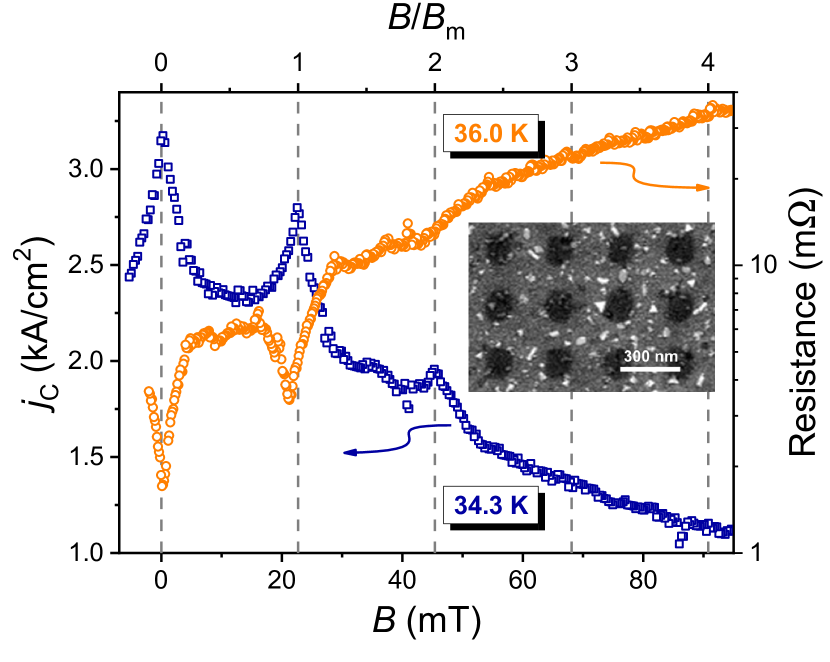
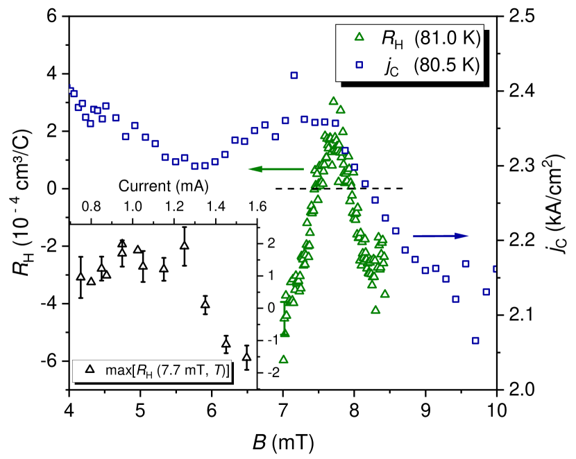
As an example of commensurability effects in the longitudinal electrical transport properties, the critical current density and the resistance of sample A ( nm) as a function of the magnetic field oriented perpendicular to the sample surface is shown in Fig. 1. To allow for a quasiequilibrium arrangement of vortices the data are collected with the respective magnetic field applied at 100 K before cooling the sample below for every datum Haag et al. (2014). The distinct maxima in and respective minima in are positioned at multiples of the matching field mT, according to Eq. (1) and taking the lattice parameter from measurements of the stencil mask in a scanning electron microscope (SEM). Interestingly, the positions of the peaks in and the minima in coincide almost perfectly, despite that they are recorded at different temperatures and the former is static, whereas the latter is a dynamic probe of vortex commensurability effects. Similar demonstrations of vortex matching effects in thin YBCO films have been reported before Castellanos et al. (1997); Swiecicki et al. (2012); Trastoy et al. (2013); Haag et al. (2014); Zechner et al. (2017a).
Correspondingly, sample B ( nm) shows a peak in at mT (obtained from a fit with background subtraction), where mT, calculated from Eq. (1) using the mask’s geometry as determined by SEM. The slight discrepancy is due to a broader and less pronounced matching peak because the intrinsic pinning of the YBCO films becomes more important at the wider CDA lattice and also to some uncertainty in the absolute values of the rather low magnetic fields.
The midpoint of the superconducting transition is lowered to K ( K) in sample A (sample B) after irradiation, probably caused by some straggling of the ions after passing through the holes in the stencil mask and within the YBCO film itself. This leads to a, although minor, number of defects in the interstitial regions between the CDs and thus a reduction of due to the -wave symmetry of the superconducting gap in YBCO. A similar observation was reported by other authors Swiecicki et al. (2012). Previous full-area irradiation experiments of YBCO films with He+ ions Sefrioui et al. (2001); Lang et al. (2004) revealed that the carrier concentration remains unchanged and the irradiation does not lead to underdoping. The Hall effect remains positive in the normal state but the carrier mobility is reduced with increasing irradiation fluence Lang et al. (2004). Hence, the observation of high-mobility electron pockets in the Fermi surface of underdoped YBCO that provokes a sign change of the Hall coefficient at intense magnetic fields LeBoeuf et al. (2007) is not relevant for our present experiments.
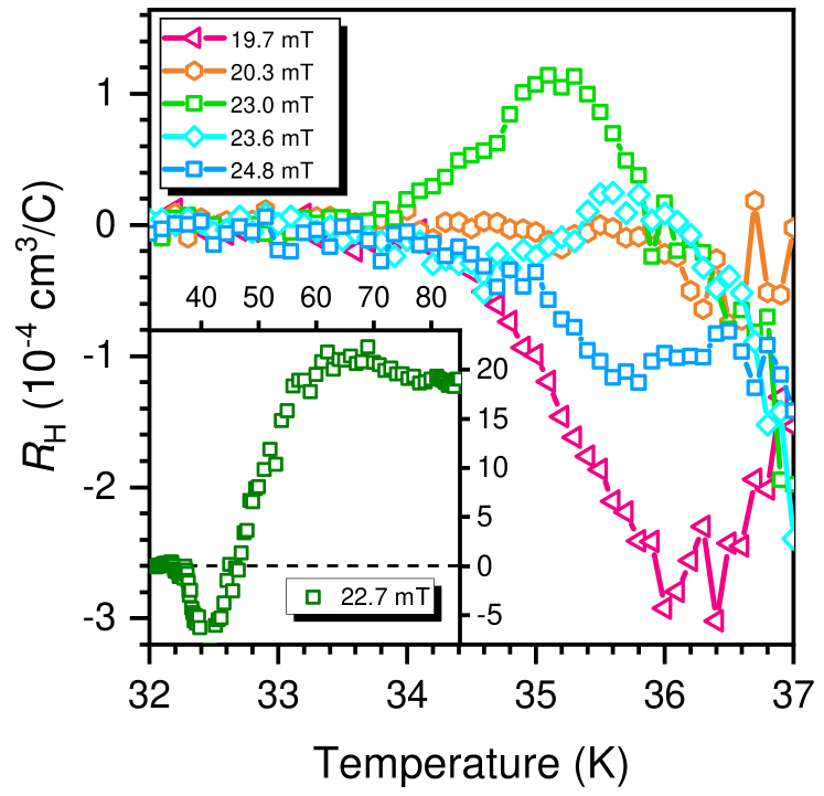
The Hall effect in sample A around the superconducting transition in an applied magnetic field that corresponds to the matching field mT is displayed in the inset of Fig. 2. At first sight, the temperature dependence of looks similar to what is found in pristine YBCO films Lang et al. (1994). The reversal of the Hall effect’s sign in the vicinity of the normal to superconducting transition is generally observed at low and moderate magnetic fields and will be considered an intrinsic effect in this paper, although its explanation is still not consensual Puica et al. (2004).
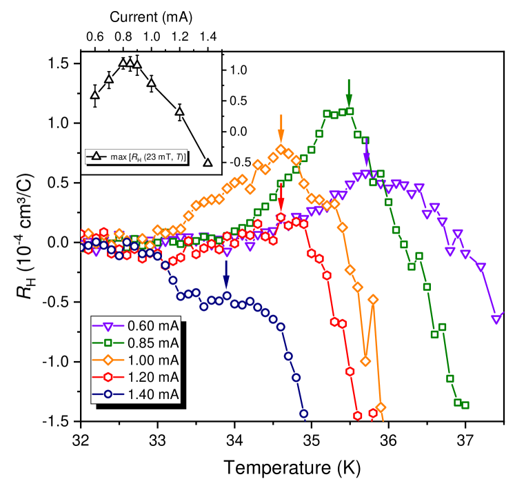
Closer inspection of the emergence of the Hall signal when pinning is overcome reveals a strikingly different behavior upon small variations of the magnetic field Zechner et al. (2017b). Whereas close to the matching field, arises with positive sign, it comes up negative otherwise (see Fig. 2). At higher temperatures, the curves merge into the one shown in the inset of Fig. 2.
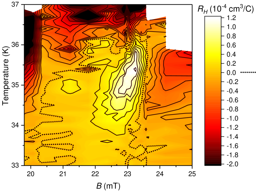
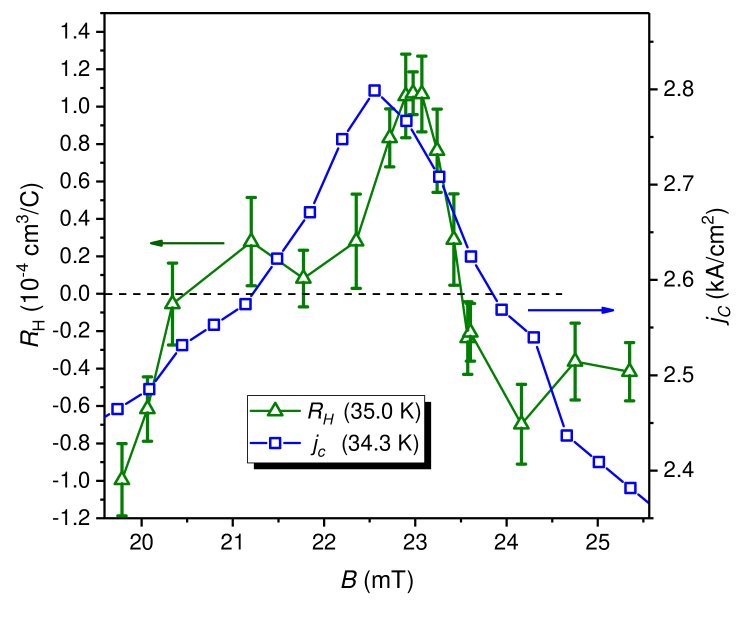
Figure 3 provides a comprehensive overview of the Hall effect in various magnetic fields around and at different temperatures. Lighter colors represent a larger positive , darker colors a larger modulus of negative and the dotted line marks the bifurcation between emergent Hall effects of different sign. Evidently, peaks around at temperatures K, corresponding to a reduced temperature range of . Outside the parameter range enveloped by the dotted line, is zero or negative up to K, where it turns positive, characteristic for the normal state.
The peak in the Hall signal is compared to the well-established signature of vortex matching by a peak in in Fig. 4 for sample A and in Fig. 6 for sample B. By appropriate scaling it is possible to almost collapse the and curves onto each other in sample A, whereas the Hall peak is somewhat sharper in sample B. This indicates that commensurability effects in the Hall channel might be even more pronounced than for longitudinal transport.
To the best of our knowledge, a sign change of the Hall effect in a superconductor with a regular pinning array, limited to a narrow region around , has not been observed before in other kinds of samples. However, additional sign changes of or the Hall conductivity have been reported in HgBa2CaCu2O6 after heavy-ion irradiation Kang et al. (2000) and in YBCO films in low magnetic fields due to pinning along twin boundaries Göb et al. (2000). Also, significant changes of due to pinning at twin boundaries have been revealed in YBCO single crystals D’Anna et al. (1998). These reports suggest that pinning can have an even stronger influence on the Hall channel than on the longitudinal transport, but they have considered disordered pinning sites only. The central result of our paper is the observation of a commensurate Hall effect peak and sign change appearing at the matching field only.
Since the observed effect is rather small and, in general, Hall effect measurements in the mT range are delicate, a careful assessment of possible spurious effects is mandatory. Due to the large amount of data [16 independent curves] represented in Fig. 3 and the effect’s reproducibility in another sample with a different CDA an erratic effect can be ruled out. Typical 95 % confidence intervals (assuming a normal distribution) calculated from data of the multiple reversals of current and magnetic field are displayed as error bars in Figs. 4–6 and confirm the relevance of our observations.
Nevertheless, a systematic error could arise from a slight misalignment of the transverse voltage probes, resulting in a transverse voltage drop originating from the longitudinal resistance, which is probed by the voltage . Together with an asymmetry of the applied magnetic field this could mimic a Hall voltage. For sample A, in the normal state above 100 K, T, nV, and thus a possible erroneous Hall voltage nV—much smaller than nV.
Another effect that might be confused with our present observation of a Hall voltage is the occurrence of a transverse voltage due to guided vortex motion in patterned superconductors. For instance, in superconductors patterned with oblique microchannels for easy vortex flow, a substantial transverse voltage has been reported Laviano et al. (2010) and confirmed that it vanishes when the easy channel is oriented parallel or perpendicular to the Lorentz force on the vortices Dobrovolskiy et al. (2016). Similarly, square arrays of antidots Silhanek et al. (2003); Wördenweber et al. (2004) or ferromagnetic dots Villegas et al. (2003), tilted with respect to the Lorentz force, allow for directional vortex channeling. Note that such guiding effects will result in an “even” Hall effect, , which can be experimentally distinguished from the conventional (odd) Hall effect, albeit the combination of guiding and disordered pinning mechanisms can evoke an odd Hall voltage, too Kopnin and Vinokur (1999); Shklovskij and Dobrovolskiy (2006).
Vortex guiding effects were reported to result in minima of at multiples of due to enhanced commensurate pinning Chialvo et al. (2005), in sharp contrast to the maxima of the Hall effect that coincide with maxima in pinning strength, reflected by the peaks in , as it is observed in our experiment (see Figs. 4 and 6). Finally, in our experimental design particular care was exercised to avoid guiding effects by orienting the main axes of the CDA parallel to the current and to the Lorentz force, respectively. In addition, we could not trace an even Hall voltage in our measurements, which makes it unlikely that guiding of vortices does influence our observations.
Furthermore, vortex flow rectification effects are predicted in arrays of pins with asymmetric shape Olson Reichhardt and Reichhardt (2005); Savel’ev et al. (2005) and in hexagonal lattices of symmetric pins with a spacial gradient Reichhardt and Olson Reichhardt (2016). Such effects can lead to a transverse voltage, which, however, would be canceled out by our measurement protocol that includes current and magnetic field reversal for every datum. Also, the necessary symmetry breaking is absent in our CDA.
The above considerations suggest that the commensurability peak and the sign change of are related to the dynamic interaction of itinerant vortices with the pinning landscape of the CDA near the borderline where thermal activation can overcome the vortex pinning. To this end, an investigation of the nonlinearity of the observed effects by varying the current through the sample is illustrative and is shown in Fig. 5 for sample A and in the inset of Fig. 6 for sample B. The value of the local maximum of rapidly decreases with larger currents in both samples, pointing to the relevance of pinning, and eventually the Hall peak disappears at larger vortex velocities. Interestingly, a slight reduction of the peak can be seen also towards lower currents, but it has to be cautioned against experimental uncertainty, which increases under these low signals. Note that the reduction of the commensurability peak is in contrast to the intrinsic negative anomalous Hall effect, which becomes more prominent and extends to a wider temperature range in high currents Lang et al. (2001); Puica et al. (2009).
IV Discussion
The problem of vortex commensurability effects in the Hall channel has not been directly addressed so far. In conjunction with the anomalous negative Hall effect, observed in most HTSCs, it has been pointed out that the complex behavior of the Hall effect results from various additive contributions to the Hall conductivity , where represents a quasiparticle or vortex-core contribution, is a superconducting contribution, resulting from hydrodynamic vortex effects and superconducting fluctuations, van Otterlo et al. (1995); Dorsey and Fisher (1992); Troy and Dorsey (1993); Kopnin et al. (1993); Nishio and Ebisawa (1997) and allows for a pinning dependence of . The sign of is the same as that of the normal-state Hall effect, i.e., positive in YBCO, but the sign of depends on details of the Fermi surface Dorsey and Fisher (1992); Troy and Dorsey (1993); Kopnin et al. (1993); van Otterlo et al. (1995); Nagaoka et al. (1998); Berg et al. (2015). The Hall effect’s sign reversal and behavior in a wide range of magnetic fields in unpatterned HTSCs can be quantitatively modeled Puica et al. (2004).
The pinning contribution can evoke a second sign reversal of , provided that it has the opposite sign of and a similar magnitude. Kopnin and Vinokur Kopnin and Vinokur (1999) have proposed such a scenario in twinned YBCO films and Ikeda Ikeda (1999) has emphasized that the sign of does depend on the dimensionality of the pinning, namely for a vortex glass with point like disordered pinning sites and for a Bose glass, when disordered line like pinning centers dominate.
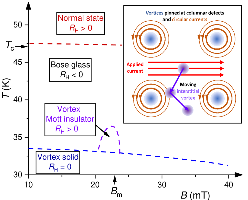
In our samples the situation is related but somewhat different from the above-mentioned models. Our observations are summarized in a schematic phase diagram of the Hall effect in Fig. 7. Lowering the temperature across leads to the aforementioned sign change of from its positive normal-state value to a negative one in a Bose glass phase. Note that this sign change roughly coincides with the midpoint at zero field. At lower temperatures, the system might undergo a transition to a vortex Mott insulator state that is confined to a region around the matching field. There, the majority of vortices are trapped in the CDA, but nevertheless a few interstitial vortices are present, dominating the transport properties, and evoking the peak of in the B-T plane displayed in Fig. 3. This regime is determined by several boundary conditions. Along the axis, vortex trapping is maximized at the commensurability field . In the temperature regime, the vortex Hall effect approaches zero when all vortices are strongly pinned into a vortex solid and, at higher temperatures, the vortex Mott insulator state is gradually destroyed by thermal fluctuations leading to an increasing number of interstitial vortices with an intrinsically negative . Hence, the positive peak of the Hall effect is limited to a rather narrow temperature interval.
A possible scenario for the sign change of in a vortex Mott insulator is sketched in the inset of Fig. 7. Nakai et al. Nakai et al. (2011) have proposed that moving vortices are deflected from their intrinsic trajectories by the circular currents surrounding pinned vortices. Their simulations revealed a sign change of the Hall voltage for disordered pinned vortex arrangements. The effect might be even enhanced in a regular array of pinned vortices—a situation that arises at the matching field in our sample. Note that the negative Hall effect implies an upstream component of vortex motion with respect to the applied current. This approach is somewhat related to the concept of the Magnus force acting on moving vortices due to an interaction of circular shielding currents with the laminar transport current Ao and Thouless (1993); Sonin (1997); Zhu et al. (1997). When the commensurable vortex arrangement is destroyed by either an off-matching external field or in high current densities, the number of mobile interstitial vortices is larger and their intrinsic Hall behavior prevails. Tuning the system between such different states of vortex matter might thus change the delicate vortex dynamics in the Hall channel and lead to the observed sign change of the Hall effect at .
Alternative scenarios of deviations of vortex trajectories from their preferred direction parallel to the Lorentz force have been considered, too. Giamarchi and Le Doussal Giamarchi and Le Doussal (1996) have proposed a transverse critical current for a moving vortex glass, and simulations by Reichhardt and co-workers Reichhardt et al. (1998); Reichhardt and Zimányi (2000) have identified a transverse critical force in a smectic vortex phase existing in superconductors with regular pinning arrays and related transverse commensurability effects with the number of moving rows of vortices between neighboring rows of pinning sites Reichhardt and Olson Reichhardt (2008). Kolton et al. Kolton et al. (1999) have predicted a Hall noise in driven vortex lattices, which disappears at high driving forces, in some agreement with our results presented in Figs. 5 and 6. Although these theoretical approaches predict transverse displacements of individual vortices or vortex channels, they are of arbitrary nature and would average out at the time scales of our transport measurements.
To provide the necessary symmetry breaking in the problem of moving vortex ensembles that can produce a finite Hall voltage, a Hall term has to be considered in the equation of motion of a vortex, as it is for instance incorporated in the Bardeen-Stephen model Bardeen and Stephen (1965). Considering the Magnus force is another option, but little is known about the Magnus force in a vortex system with a regular pinning array. Along these lines, our observation of a commensurability peak in the Hall effect in superconductors with a pin lattice might spark additional theoretical efforts to develop a more detailed picture of vortex motion in regular pin arrays by including additional force terms.
V Conclusions
A regular array of defect columns in thin YBCO films not only gives rise to maxima in the critical current and minima in the resistance, but also to a manifestation of commensurability in the transverse Hall signal. A peak of the Hall coefficient and a related sign change from its intrinsic negative values in the mixed state to positive appear in a narrow magnetic field range around the matching field. Previous theoretical results have predicted a sign change of the Hall signal due to strong pinning of a vortex Bose glass but no predictions have been made for the vortex Hall effect in a superconductor with a regular pinning array and for the Hall effect near a vortex Mott metal/insulator transition. We have confirmed that our findings are not related to guided vortex motion and instead suggest that the transverse Hall voltage can be a subtle probe for vortex dynamics in a periodic pinning landscape that needs further attention.
Acknowledgments
We appreciate the help of K. Haselgrübler with the ion implanter. Illuminating discussions with V. M. Vinokur, A. Silhanek, R. Wördenweber, and O. V. Dobrovolskiy are acknowledged. This article is based upon work from COST Action CA16218 (NANOCOHYBRI), supported by COST (European Cooperation in Science and Technology). M.D. acknowledges the European Erasmus Mundus (Target II) program for financial support.
References
- Bardeen and Stephen (1965) J. Bardeen and M. Stephen, Phys. Rev. 140, A1197 (1965).
- Nozières and Vinen (1966) P. Nozières and W. F. Vinen, Phil. Mag. 14, 667 (1966).
- Kopnin (2002) N. B. Kopnin, Rep. Prog. Phys. 65, 1633 (2002).
- Sonin (1997) E. B. Sonin, Phys. Rev. B 55, 485 (1997).
- Ao and Thouless (1993) P. Ao and D. J. Thouless, Phys. Rev. Lett. 70, 2158 (1993).
- Zhu et al. (1997) X. M. Zhu, E. Brändström, and B. Sundqvist, Phys. Rev. Lett. 78, 122 (1997).
- Ao (1998) P. Ao, J. Phys.: Condens. Matter 10, L677 (1998).
- Galffy and Zirngiebl (1988) M. Galffy and E. Zirngiebl, Solid State Commun. 68, 929 (1988).
- Nagaoka et al. (1998) T. Nagaoka, Y. Matsuda, H. Obara, A. Sawa, T. Terashima, I. Chong, M. Takano, and M. Suzuki, Phys. Rev. Lett. 80, 3594 (1998).
- Lang et al. (1994) W. Lang, G. Heine, P. Schwab, X. Z. Wang, and D. Bäuerle, Phys. Rev. B 49, 4209 (1994).
- Nishio and Ebisawa (1997) T. Nishio and H. Ebisawa, Physica C 290, 43 (1997).
- Puica et al. (2004) I. Puica, W. Lang, W. Göb, and R. Sobolewski, Phys. Rev. B 69, 104513 (2004), and references therein.
- Fukuyama et al. (1971) H. Fukuyama, H. Ebisawa, and T. Tsuzuki, Prog. Theor. Phys. 46, 1028 (1971).
- Dorsey (1992) A. T. Dorsey, Phys. Rev. B 46, 8376 (1992).
- van Otterlo et al. (1995) A. van Otterlo, M. Feigel’man, V. Geshkenbein, and G. Blatter, Phys. Rev. Lett. 75, 3736 (1995).
- Berg et al. (2015) E. Berg, S. D. Huber, and N. H. Lindner, Phys. Rev. B 91, 024507 (2015).
- Wang and Ting (1991) Z. D. Wang and C. S. Ting, Phys. Rev. Lett. 67, 3618 (1991).
- Vinokur et al. (1993) V. M. Vinokur, V. B. Geshkenbein, M. V. Feigel’man, and G. Blatter, Phys. Rev. Lett. 71, 1242 (1993).
- Wang et al. (1994) Z. D. Wang, J. M. Dong, and C. S. Ting, Phys. Rev. Lett. 72, 3875 (1994).
- Kopnin and Vinokur (1999) N. B. Kopnin and V. M. Vinokur, Phys. Rev. Lett. 83, 4864 (1999).
- Nakai et al. (2011) N. Nakai, N. Hayashi, and M. Machida, Phys. Rev. B 83, 024507 (2011).
- Ikeda (1999) R. Ikeda, Physica C 316, 189 (1999).
- Göb et al. (2000) W. Göb, W. Liebich, W. Lang, I. Puica, R. Sobolewski, R. Rössler, J. D. Pedarnig, and D. Bäuerle, Phys. Rev. B 62, 9780 (2000).
- Lang et al. (2001) W. Lang, W. Göb, J. D. Pedarnig, R. Rössler, and D. Bäuerle, Physica C 364-365, 518 (2001).
- D’Anna et al. (1998) G. D’Anna, V. Berseth, L. Forró, A. Erb, and E. Walker, Phys. Rev. Lett. 81, 2530 (1998).
- Moshchalkov et al. (2010) V. V. Moshchalkov, R. Wördenweber, and W. Lang, eds., Nanoscience and Engineering in Superconductivity (Springer, Heidelberg, 2010).
- Harada et al. (1996) K. Harada, O. Kamimura, H. Kasai, T. Matsuda, A. Tonomura, and V. V. Moshchalkov, Science 274, 1167 (1996).
- Baert et al. (1995) M. Baert, V. V. Metlushko, R. Jonckheere, V. V. Moshchalkov, and Y. Bruynseraede, Phys. Rev. Lett. 74, 3269 (1995).
- Lykov (1993) A. N. Lykov, Solid State Commun. 86, 531 (1993).
- Fiory et al. (1978) A. T. Fiory, A. F. Hebard, and S. Somekh, Appl. Phys. Lett. 32, 73 (1978).
- Nelson and Vinokur (1993) D. R. Nelson and V. M. Vinokur, Phys. Rev. B 48, 13060 (1993).
- Goldberg et al. (2009) S. Goldberg, Y. Segev, Y. Myasoedov, I. Gutman, N. Avraham, M. Rappaport, E. Zeldov, T. Tamegai, C. W. Hicks, and K. A. Moler, Phys. Rev. B 79, 064523 (2009).
- Jiang et al. (2004) Z. Jiang, D. A. Dikin, V. Chandrasekhar, V. V. Metlushko, and V. V. Moshchalkov, Appl. Phys. Lett. 84, 5371 (2004).
- Poccia et al. (2015) N. Poccia, T. I. Baturina, F. Coneri, C. G. Molenaar, X. R. Wang, G. Bianconi, A. Brinkman, H. Hilgenkamp, A. A. Golubov, and V. M. Vinokur, Science 349, 1202 (2015).
- Lang et al. (2006) W. Lang, M. Dineva, M. Marksteiner, T. Enzenhofer, K. Siraj, M. Peruzzi, J. D. Pedarnig, D. Bäuerle, R. Korntner, E. Cekan, E. Platzgummer, and H. Loeschner, Microelectron. Eng. 83, 1495 (2006).
- Lang et al. (2009) W. Lang, H. Richter, M. Marksteiner, K. Siraj, M. A. Bodea, J. D. Pedarnig, C. Grigoropoulos, and D. Bäuerle, Int. J. Nanotechnol. 6, 704 (2009).
- Pedarnig et al. (2010) J. D. Pedarnig, K. Siraj, M. A. Bodea, I. Puica, W. Lang, R. Kolarova, P. Bauer, K. Haselgrübler, C. Hasenfuss, I. Beinik, and C. Teichert, Thin Solid Films 518, 7075 (2010).
- Zechner et al. (2017a) G. Zechner, F. Jausner, L. T. Haag, W. Lang, M. Dosmailov, M. A. Bodea, and J. D. Pedarnig, Phys. Rev. Applied 8, 014021 (2017a).
- Heine and Lang (1998) G. Heine and W. Lang, Cryogenics 38, 377 (1998).
- Haag et al. (2014) L. T. Haag, G. Zechner, W. Lang, M. Dosmailov, M. A. Bodea, and J. D. Pedarnig, Physica C 503, 75 (2014).
- Castellanos et al. (1997) A. Castellanos, R. Wördenweber, G. Ockenfuss, A. v.d. Hart, and K. Keck, Appl. Phys. Lett. 71, 962 (1997).
- Swiecicki et al. (2012) I. Swiecicki, C. Ulysse, T. Wolf, R. Bernard, N. Bergeal, J. Briatico, G. Faini, J. Lesueur, and J. E. Villegas, Phys. Rev. B 85, 224502 (2012).
- Trastoy et al. (2013) J. Trastoy, V. Rouco, C. Ulysse, R. Bernard, A. Palau, T. Puig, G. Faini, J. Lesueur, J. Briatico, and J. E. Villegas, New J. Phys. 15, 103022 (2013).
- Sefrioui et al. (2001) Z. Sefrioui, D. Arias, E. M. Gonzalez, C. Leon, J. Santamaria, and J. L. Vicent, Phys. Rev. B 63, 064503 (2001).
- Lang et al. (2004) W. Lang, T. Enzenhofer, M. Peruzzi, J. D. Pedarnig, D. Bäuerle, C. Horner, E. Cekan, E. Platzgummer, and H. Loeschner, Inst. Phys. Conf. Ser. 181, 1549 (2004).
- LeBoeuf et al. (2007) D. LeBoeuf, N. Doiron-Leyraud, J. Levallois, R. Daou, J. B. Bonnemaison, N. E. Hussey, L. Balicas, B. J. Ramshaw, R. X. Liang, D. A. Bonn, W. N. Hardy, S. Adachi, C. Proust, and L. Taillefer, Nature 450, 533 (2007).
- Zechner et al. (2017b) G. Zechner, L. T. Haag, W. Lang, M. Dosmailov, M. A. Bodea, and J. D. Pedarnig, Physica C 533, 144 (2017b).
- Kang et al. (2000) W. N. Kang, B. W. Kang, Q. Y. Chen, J. Z. Wu, Y. Bai, W. K. Chu, D. K. Christen, R. Kerchner, and S. I. Lee, Phys. Rev. B 61, 722 (2000).
- Laviano et al. (2010) F. Laviano, G. Ghigo, E. Mezzetti, E. Hollmann, and R. Wördenweber, Physica C 470, 844 (2010).
- Dobrovolskiy et al. (2016) O. V. Dobrovolskiy, M. Hanefeld, M. Zörb, M. Huth, and V. A. Shklovskij, Supercond. Sci. Technol. 29, 065009 (2016).
- Silhanek et al. (2003) A. V. Silhanek, L. Van Look, S. Raedts, R. Jonckheere, and V. V. Moshchalkov, Phys. Rev. B 68, 214504 (2003).
- Wördenweber et al. (2004) R. Wördenweber, P. Dymashevski, and V. R. Misko, Phys. Rev. B 69, 184504 (2004).
- Villegas et al. (2003) J. E. Villegas, E. M. Gonzalez, M. I. Montero, I. K. Schuller, and J. L. Vicent, Phys. Rev. B 68, 224504 (2003).
- Shklovskij and Dobrovolskiy (2006) V. A. Shklovskij and O. V. Dobrovolskiy, Phys. Rev. B 74, 104511 (2006).
- Chialvo et al. (2005) C. E. Chialvo, J. Guimpel, S. Reparaz, and H. Pastoriza, Physica C 422, 112 (2005).
- Olson Reichhardt and Reichhardt (2005) C. J. Olson Reichhardt and C. Reichhardt, Physica C 432, 125 (2005).
- Savel’ev et al. (2005) S. Savel’ev, V. Misko, F. Marchesoni, and F. Nori, Phys. Rev. B 71, 214303 (2005).
- Reichhardt and Olson Reichhardt (2016) C. Reichhardt and C. J. Olson Reichhardt, Phys. Rev. B 93, 064508 (2016).
- Puica et al. (2009) I. Puica, W. Lang, K. Siraj, J. D. Pedarnig, and D. Bäuerle, Phys. Rev. B 79, 094522 (2009).
- Dorsey and Fisher (1992) A. T. Dorsey and M. P. A. Fisher, Phys. Rev. Lett. 68, 694 (1992).
- Troy and Dorsey (1993) R. J. Troy and A. T. Dorsey, Phys. Rev. B 47, 2715 (1993).
- Kopnin et al. (1993) N. B. Kopnin, B. I. Ivlev, and V. A. Kalatsky, J. Low Temp. Phys. 90, 1 (1993).
- Giamarchi and Le Doussal (1996) T. Giamarchi and P. Le Doussal, Phys. Rev. Lett. 76, 3408 (1996).
- Reichhardt et al. (1998) C. Reichhardt, C. J. Olson, and F. Nori, Phys. Rev. B 58, 6534 (1998).
- Reichhardt and Zimányi (2000) C. Reichhardt and G. T. Zimányi, Phys. Rev. B 61, 14354 (2000).
- Reichhardt and Olson Reichhardt (2008) C. Reichhardt and C. J. Olson Reichhardt, Phys. Rev. B 78, 180507(R) (2008).
- Kolton et al. (1999) A. B. Kolton, D. Domínguez, and N. Grønbech-Jensen, Phys. Rev. Lett. 83, 3061 (1999).