Computational study of heavy group IV elements (Ge, Sn, Pb) triangular lattice atomic layers on SiC(0001) surface
Abstract
Group IV heavy elements atomic layers are expected to show an interesting physical properties due to their large spin-orbit coupling (SOC). Using density functional theory (DFT) calculations with/without SOC we investigate the variation of group IV heavy elements overlayers, namely dense triangular lattice atomic layers (TLAL) on the surface of SiC(0001) semiconductor. The possibility of such layers formation and their properties have not been addressed before. Here we show, that these layers may indeed be stable and, owing to peculiar bonding configuration, exhibit robust Dirac-like energy bands originating from orbitals and localized mostly within the layer, and band localized outside the layer and interacting with SiC substrate. We found that a adsorption site is most favorable for such TLAL structure and this results in an unusual SOC-induced spin polarization of the states around points of Brillouin zone, namely the coexistence of Rashba- and Zeeman-like spin polarization of different states. We explain this phenomena in terms of symmetry of partial electronic density rather than symmetry of atomic structure.
pacs:
71.15.Dx, 73.20.At, 73.61.AtI Introduction
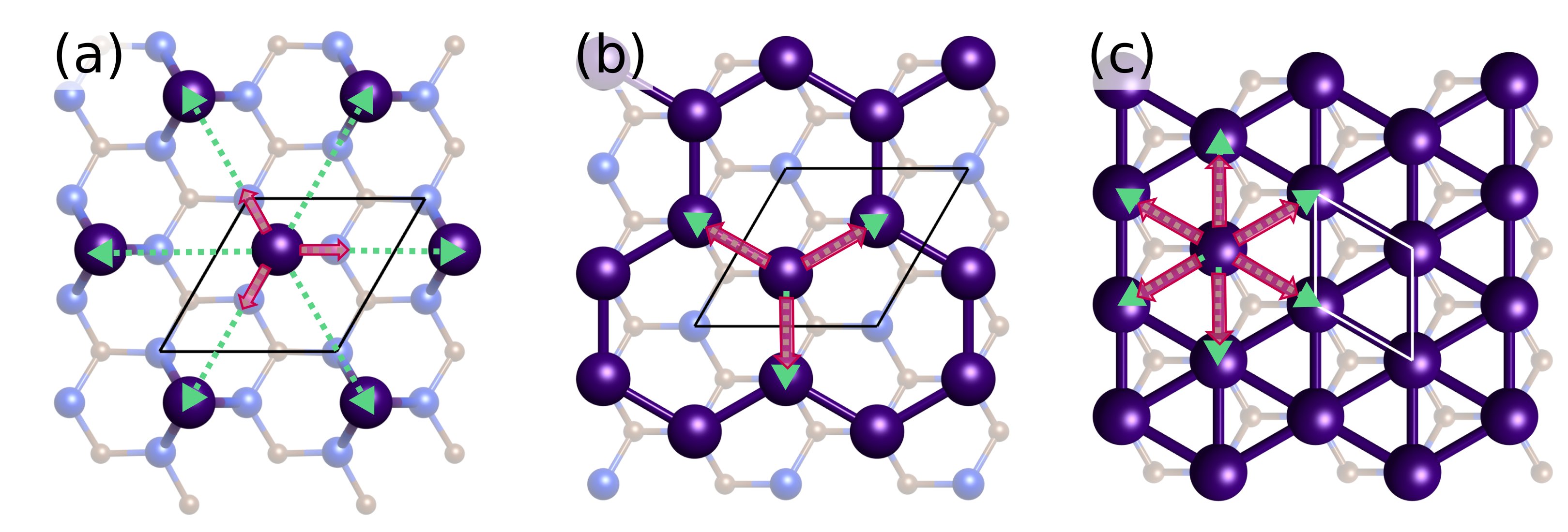
Two-dimensional (2D) metal overlayers on semiconductor surfaces are excellent model systems for studying various quantum mechanics phenomena. Specifically, group IV heavy elements (Ge, Sn, Pb) triangular lattices on hexagonal semiconductor surfaces, especially Si(111) and Ge(111), are a long time study objects of surface scientistsOdobescu et al. (2017); Cortés et al. (2006); Profeta and Tosatti (2007); Lee et al. (2013); Badrtdinov et al. (2016); M. et al. (1996). Surface charge density waves (CDW) were first observed by scanning tunneling microscopy (STM) in -Pb overlayer on Ge(111)M. et al. (1996). While by simple electron count adatom overlayers of group IV elements should be metallic, many of them exhibit insulating properties. This was explained by strong electron correlation and Mott- or Slater-type metal–insulator transitionProfeta and Tosatti (2007); Lee et al. (2013); Badrtdinov et al. (2016). The particular type of such transition is still under debate. As triangular arrangement of magnetic moments results in frustration, spin liquid phase has been expected to show up in these systemsFazekas and Anderson (1974). Experimentally, however, the spontaneous magnetic ordering has been observedLi et al. (2013). Also, as heavy elements exhibit strong spin-orbit coupling (SOC), metallic overlayers show significant Rashba spin-polarization of electronic states, tunable both by choice of suitable substrate and by applying external gate voltageSlomski et al. (2013), making these structures advantageous in terms of application in spintronic devices. Typical adatom arrangement, however, is rather sparse (see Fig. 1(a)). The adatoms are separated by significant distance ( Å), so no direct in-plane bonding exists in these structures. The electronic properties are governed by large-distance electron hopping and interaction via substrate. If the atomic density of such overlayer is increased by adding one more metal atom, this will result in honeycomb structure (Fig. 1(b)). In honeycomb arrangement the atoms do interact directly, forming in-plane bonds. Honeycomb lattice results in formation of Dirac cone-like electron dispersion exhibiting many exotic properties similar to those of graphene and beyond. Group IV elements honeycomb overlayers such as germanene Li et al. (2014); Zhang et al. (2016), staneneXu et al. (2013); Wu et al. (2014); feng Zhu et al. (2015), and plumbeneYu et al. (2017); Zhao et al. (2016) have boomed recently in number of experimental and theoretical works. Yet, these are still difficult to grow on semiconductor surfaces and were mostly synthesized on metals, making it less suitable for direct device applications. Further increase in atomic density by adding one more atom will result again in triangular structure (Fig. 1(c)). This, however, is rather different from phase mentioned previously. In such a dense triangular lattice atoms are very close to each other ( Å), making direct in-plane bonding possible. The bonding configuration in such system is very peculiar. Each metal atom has six nearest neighbours, while typically group IV elements tend to form three or four covalent bonds, depending on orbital hybridization. This may result in layers with new interesting physics and useful properties. While undoubtedly interesting, the properties of such systems are mostly unexplored, mainly due to the lack of experimentally observed structures of this type. The only reports of closely related systems are Si(111)--TlNoda et al. (2003); Kim et al. (2004) and high-density Si(111)- and Ge(111)--PbHuang et al. (1989); Ren et al. (2016); Brand et al. (2017); Yaji et al. (2010). In thallium system adatoms sit at site of bulk-terminated Si(111) surfaceNoda et al. (2003). Due to the symmetry of the atomic structure ( symmetry at point of Brillouin zone), Tl system exhibit so-called Zeeman-type of spin-splitting of states at the point with spin direction normal to the surfaceSakamoto et al. (2009a); Nakajin and Murakami (2015). In the Pb system the one of the atom sits at site (though ab initio calculations shows that system with adatom at is just marginally higher in energy) and other three atoms are at slightly displaced locations from main symmetric adsorption sitesRen et al. (2016); Yaji et al. (2012); Ohtsubo et al. (2011). In this structure Zeeman-like splitting has been also observed at point, as well as small Rashba-type splitting at time-reversal-invariant momenta (TRIM) points ( and )Brand et al. (2017). The conventional Rashba type splitting is described by Rashba Hamiltonian , where and are Pauli matrices and in-plane wave-vector component respectively, and is a Rashba parameterBychkov and Rashba (1984). It is observed only in TRIM points of the Brillouin zone and results in in-plane spin vortexes. Some unconventional Rashba effects has been also reported to occur at non-TRIM points, such as point, for systems like Si(111)--Bi with symmetry at Sakamoto et al. (2009b). While, not being classical Rashba effect, this spin-polarization is well described by Rashba-like HamiltonianSakamoto et al. (2009b); Nakajin and Murakami (2015).
The lack of experimental evidences of dense triangular lattice atomic layers (TLALs) of group IV is due to the fact that most of up to date the adsorption experiments has been carried out on Si(111) or Ge(111) substrates, which unit cell is too large for stable TLAL formation. SiC(0001) surface, however, is much more suitable candidate for TLALs. In fact we have experimentally observed Sn TLAL structure formation at graphene/SiC(0001) interface by Sn atoms intercalationHayashi et al. (2017). In the present paper we show that dense triangular overlayers with symmetric adatoms locations are possible on bare SiC(0001) surface and discuss their peculiar electronic structure.
II Computation details
The calculations have been performed using Vienna ab initio simulation package (VASP)Kresse and Furthmüller (1996) with PAW-type pseudopotentialsBlöchl (1994); Kresse and Joubert (1999). General gradient approximation in Perdew-Burke-Ernzerhof (PBE)Perdew et al. (1996) formulation has been used for exchange and correlation. Plane wave cut-off energy was set to 500 eV. In structure optimization -point centered regular and k-space samplings were used for and structures respectively. For accurate ground state energy and electronic density calculations k-space mesh density has been increased to and , respectively. In most cases structure optimization has been performed without SOC included to save time, though several tests were performed to ensure that inclusion of SOC does not have significant influence on the resulting structure or total energy difference when comparing different structures. The structures were modelled as a slabs of 6H-SiC(0001) with six SiC bilayers, back surface saturated with hydrogen atoms, top surface covered by metal overlayer, and vacuum layer of 10 Å separating slab periodic copies. The structure optimization has been performed until maximum force is less than 0.005 eV/Å.
III Results and discussion
III.1 adsorption site
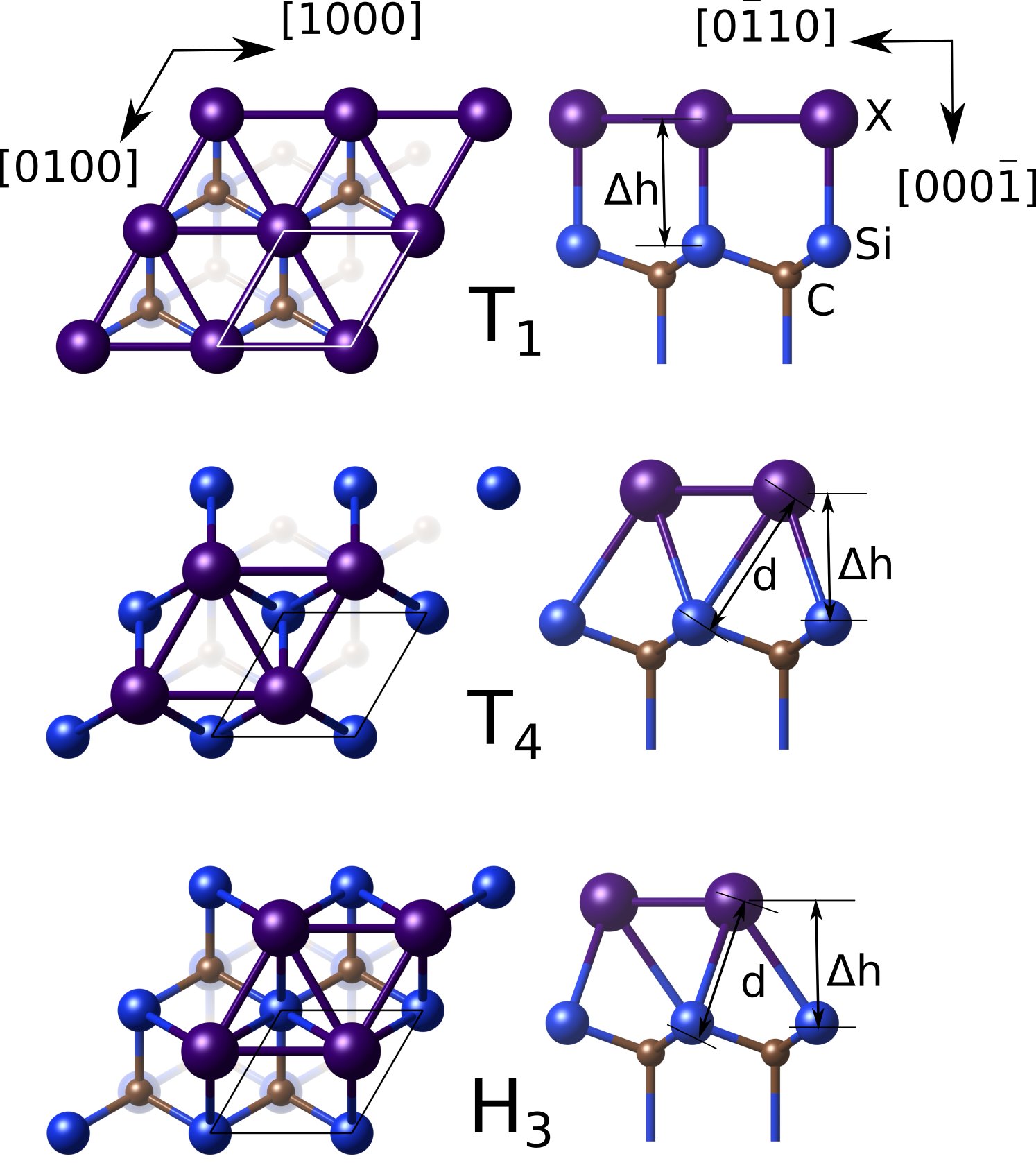
As the model for dense TLALs on SiC(0001) was initially guessed to be , which is in agreement with our previous experimental resultsHayashi et al. (2017), first we investigate different models of -X overlayers (where X is Ge, Sn, or Pb atoms) on SiC(0001). As superstructure is rather small, only limited number of structural models, distinct only by X atom adsorption site, are reasonable. Three main adsorption sites exist on hexagonal SiC(0001) surface, namely or on-top site, and tetrahedrally coordinated and sites (Fig. 2). Table 1 shows the calculated relative total energies and structural parameters for these models. For all three elements on-top site is found to be most stable by quite substantial energy difference. This is in contrast with Si(111)--Tl system, where Tl atoms theoretically and experimentally are found to occupy siteNoda et al. (2003); Kim et al. (2004). This difference has significant consequences for electronic structure as will be shown below. Interestingly interlayer distances in all three adsorption configurations are very close. This is because in structure, tetrahedrally coordinated adsorbate atoms (in or sites) have to share bonds with substrate top Si atoms, making these bonds weaker and much longer compared to strong bonds in on-top configuration, where each adsorbate atoms has one individual bond with substrate Si. Experimentally the negligible difference in interlayer distances could make it difficult to distinguish between model when layer distance sensitive only methods are used (such as X-ray truncation rod scattering analysis used in our previous experimental work Hayashi et al. (2017)).
| site | site | site | ||
| Ge | +0.67 | +0.43 | ||
| , eV | Sn | +0.51 | +0.34 | |
| Pb | +0.40 | +0.20 | ||
| Ge | 2.51 | 2.40 | 2.47 | |
| , Å | Sn | 2.71 | 2.65 | 2.59 |
| Pb | 2.81 | 2.79 | 2.71 | |
| Ge | 2.51 | 3.05 | 2.99 | |
| , Å | Sn | 2.71 | 3.20 | 3.15 |
| Pb | 2.81 | 2.79 | 2.71 |
III.2 Stability of overlayer
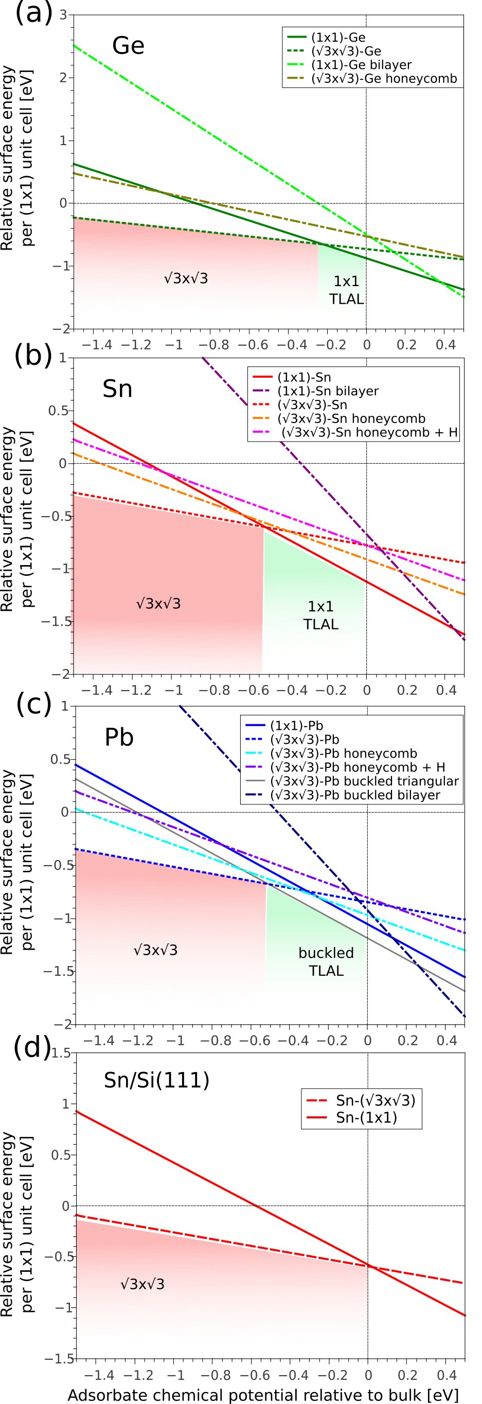
As mentioned before, one of the main reasons the properties of group IV elements triangular overlayer has not been addressed before is that, with rare exceptions, no such overlayer has been observed so far. Here we address the principal possibility of that kind of structure to exist on SiC(0001). After we have confirmed that among different models, the one with on-top adsorption site is most stable, we may compare the relative surface energy of this structure to more conventional reconstructions observed and/or proposed. That is ML adatom structure, honeycomb layer with and without hydrogen termination of the remaining dangling bonds similar to those of bismuthen reported in Ref. Reis et al., 2017, and bilayer. The -ML triangular arrangement similar to that of Pb on Si(111) or Ge(111) surfaceHuang et al. (1989); Ren et al. (2016); Brand et al. (2017); Yaji et al. (2010, 2012); Ohtsubo et al. (2011) is not considered here due to large lattice mismatch between such arrangement on much more compact SiC(0001) and equilibrium unit cell of artificial standalone TLAL (2.78, 3.16, and 3.29 Å for Ge, Sn and Pb respectively). As the different surface structures are of different adsorbate atoms coverage, one cannot compare the calculated total energies directly, but have to build dependence on adsorbate chemical potential . Relative surface energy is calculated in the following way:
| (1) |
where is relative surface energy per unit cell, – unit cell surface area (in terms cells), – total energy of a system, – energy of ideal bulk terminated SiC slab without adsorbates, – number of adsorbate atoms, and – chemical potential of atom X. The results are shown in Fig. 3 using the chemical potential scale relative to the corresponding bulk values (calculated separately). Thus, the positive values on horizontal axis mean that three-dimensional (3D) growth of bulk material is more preferable, while negative values indicate region where 2D layer is more stable. As seen from the Fig. 3 all three elements show the existence of stability region for reconstruction in the adsorbate rich conditions (the buckling case of Pb will be discussed below). In the adsorbate poor region normal adatom structure prevails. Note, that all other simple reconstructions show higher relative surface energies and should be considered unstable. For comparison in Fig. 3(d) similar calculations for Sn/Si(111) surface are shown. In this case the structure is unstable. The reason for this is substantially larger surface unit cell of 3.84 Å of Si(111) compared to 3.08 Å of SiC(0001). At such long distance the direct in-plane bonding between adsorbate atoms seems to be unfavorable with shorter equilibrium unit cells of free standing TLALs. This is one of the reasons why these structures have not been observed before, as SiC(0001) surface is much less studied experimentally than Si(111).
III.3 Buckling of triangular overlayer
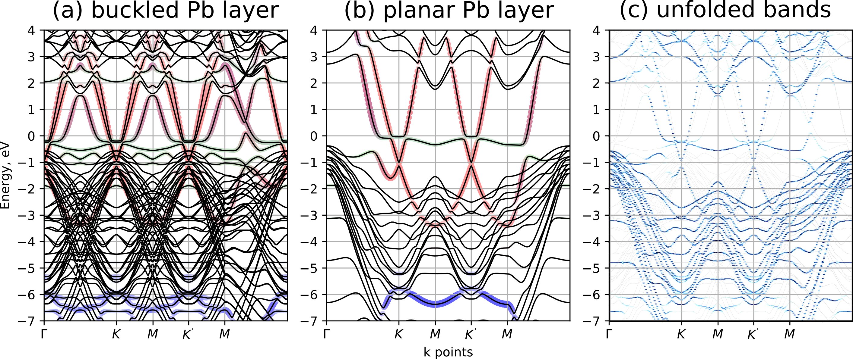
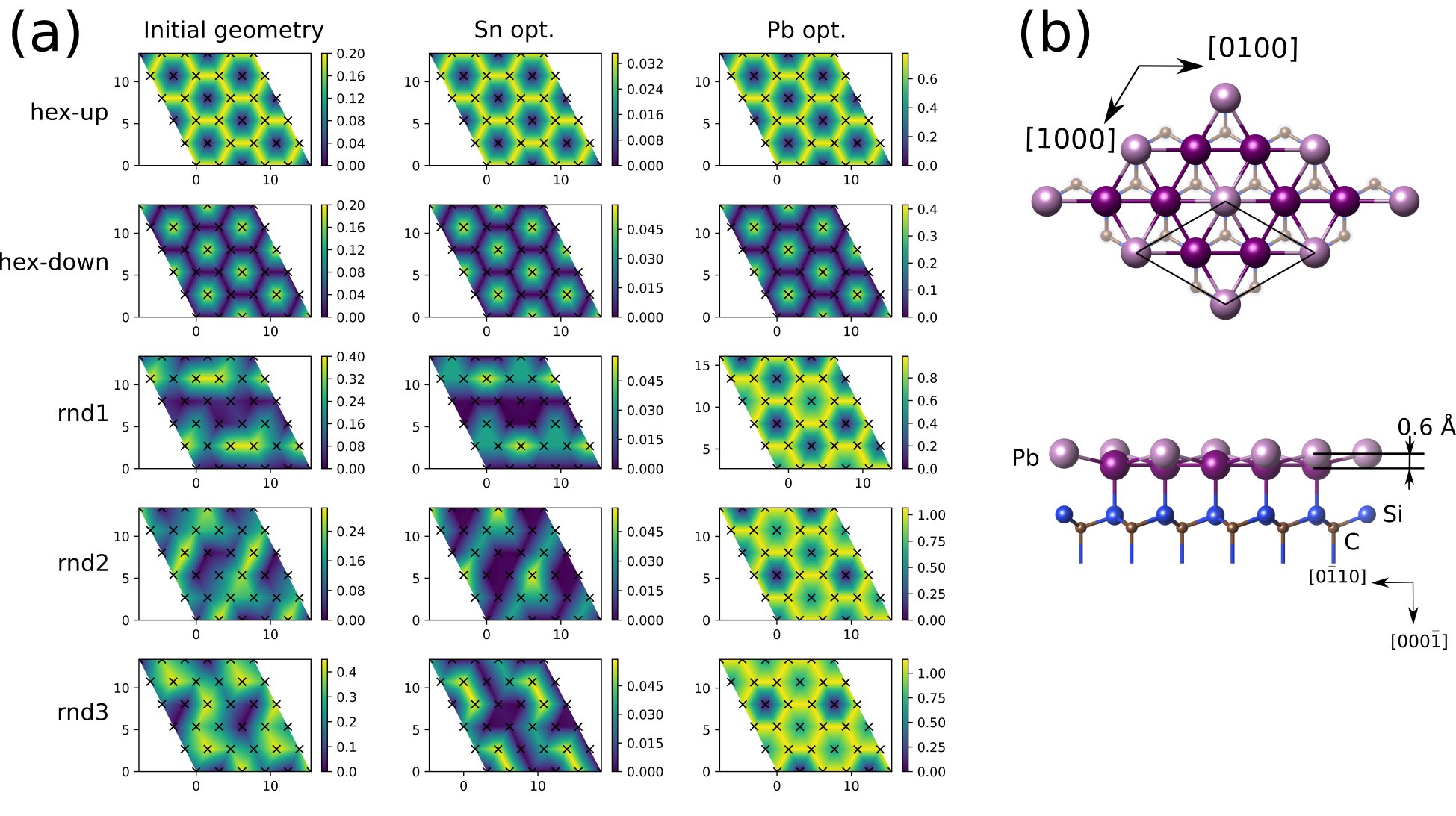
As mentioned in the previous section the equilibrium cell size of free-standing triangular metallic layer is slightly different to SiC(0001) surface unit cell size. While for Ge case the equilibrium size is smaller, so layer will be slightly stretched and planar geometry is naturally expected, this cannot be said about Sn and Pb case, which both have slightly larger equilibrium cell size ( and Å respectively). The compressive stress on a layer may lead to buckling and, as a result, increase of the actual periodicity of the overlayer structure. Thus, to check this possibility we performed calculations with large unit cells of and with regularly and randomly displaced metal atoms in vertical direction to reduce any artificially induced symmetry constrains on a system. Then, structure optimization calculations has been performed. These were repeated for several regular and random initial configurations. Fig. 4 represent a height map of adsorbate atoms before and after structure optimization. In Table 2 the energetics of different structures are compared. It is clear that the structures with higher than periodicity are formed. In the case of Sn atoms, the overlayer corrugation after structure optimization is rather small ( Å) and in most cases retain the similar height map as original structure, which is indicative for artifact of structure optimization routine (such as meeting convergence criteria before perfect arrangement is formed). Also the energy differences between ideal and larger, slightly buckled structures are negligible. Thus, we may safely assume that Sn forms non-buckled overlayer on SiC(0001). On the other hand, Pb layer optimization shows significantly buckled structure. The basic periodicity of resultant overlayer from almost all trial configurations is close to . The overlayer is represented by honeycomb planar layer plus the atom in the center of the hexagon with slightly higher vertical position ( Å) as shown in Fig. 4. As seen from the Table. 2 this reconstruction is noticeably lower in energy than , making the stability region of this dense overlayer even wider.
| Element | Trial config. | Before opt. | After opt. | |
|---|---|---|---|---|
| hex-up | , Å | 0.2 | 0.03 | |
| , eV | — | |||
| hex-down | , Å | 0.2 | 0.05 | |
| , eV | — | |||
| Sn | rnd1 | , Å | 0.4 | 0.05 |
| , eV | — | |||
| rnd2 | , Å | 0.3 | 0.05 | |
| , eV | — | |||
| rnd3 | , Å | 0.45 | 0.05 | |
| , eV | — | |||
| hex-up | , Å | 0.2 | 0.7 | |
| , eV | — | |||
| hex-down | , Å | 0.2 | 0.4 | |
| , eV | — | |||
| Pb | rnd1 | , Å | 0.4 | 0.9 |
| , eV | — | |||
| rnd2 | , Å | 0.3 | 0.9 | |
| , eV | — | |||
| rnd3 | , Å | 0.45 | 1.0 | |
| , eV | — |
III.4 Band structure
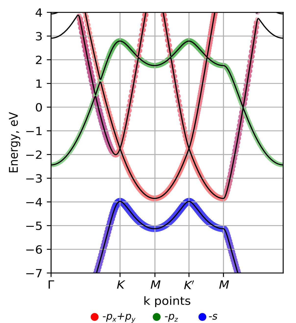
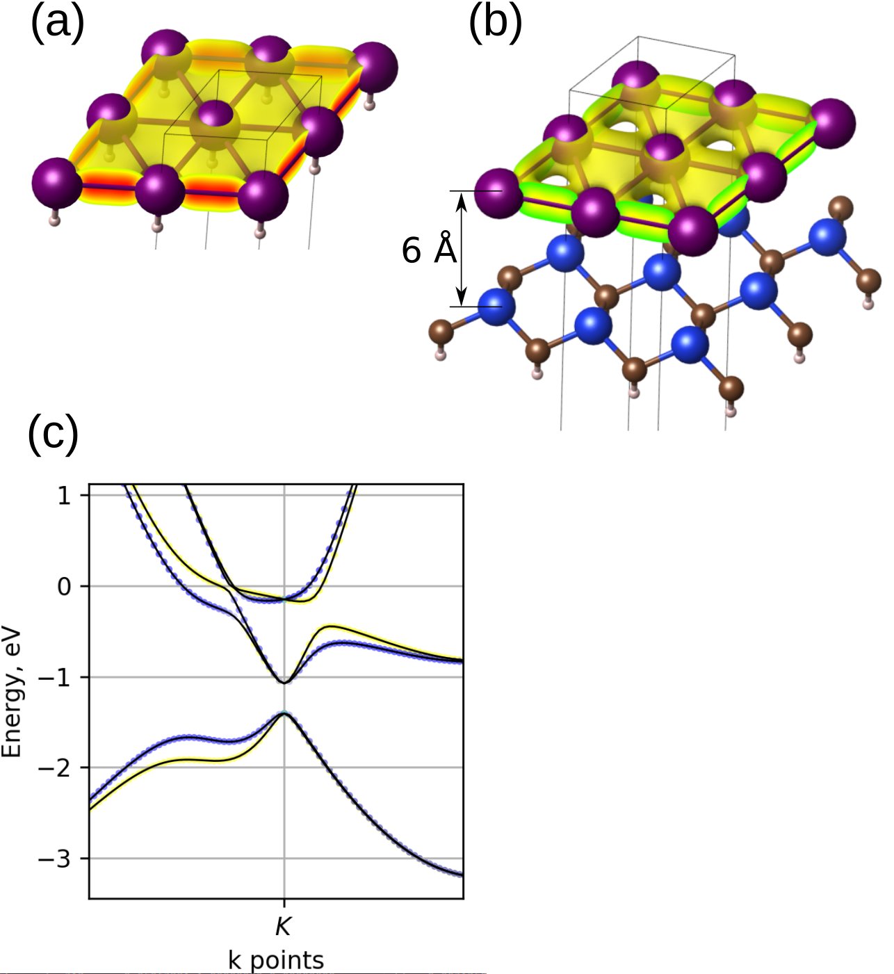
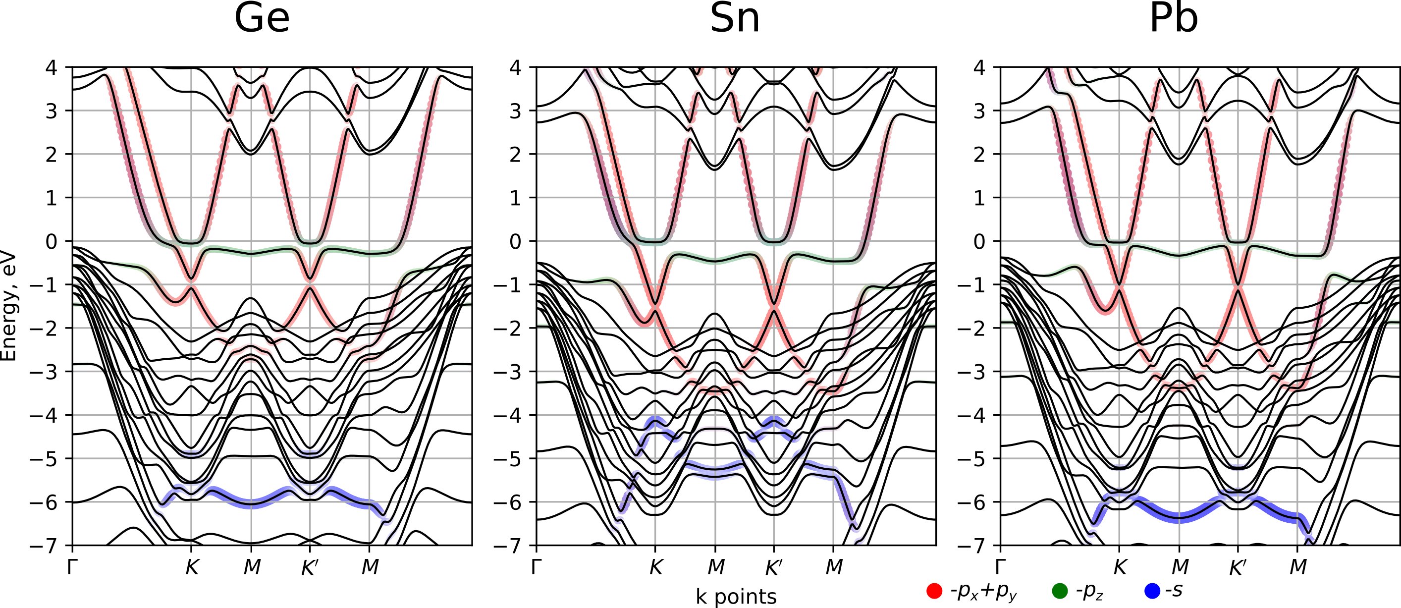
The typical calculated band structure without SOC is shown in Fig. 5. All elements exhibit qualitatively similar band structure with some variation of the energy of particular bands and values of gaps. The two main features of band structure are Dirac-cone-like dispersion at and points around eV below Fermi level and much flatter band around Fermi level. Interestingly the Dirac-like dispersion feature originate totally from and orbitals as seen from orbital projection calculation rather than orbital like in case of most honeycomb lattices. Electronic density of these bands is fully localized inside the TLAL, which makes it a perfect 2D metal (see Fig. 7(a)). The branches of Dirac-like dispersion exhibit a small gap (220 meV, 160 meV, and 130 meV for Ge, Sn, and Pb respectively). The origin of this gap is similar to the one discussed in Ref. Petersen and Hedegård, 2000, namely the braking of space inversion symmetry, which allows electron hopping from orbital (hybridized with substrate dangling bonds) states to and states. In the band structure of artificial free-standing triangular layer these gaps are absent (see Supplementarysup Fig. S1). The orbital, on the other hand, hybridize slightly with orbital and top layer Si dangling bonds and form flattish band near the Fermi level.
As discussed in previous section Pb TLAL is buckled and has periodicity rather than . This however does not influence bands structure to significant degree. If we perform unfolding procedureMedeiros et al. (2014) of band structure onto Brillouin zone, one can see that the bands are actually almost identical to those calculated for planar layer. So, for band properties we restrict our further study to planar Pb layer. The full and unfolded band structure of buckled Pb layer can be found in Supplementarysup (Fig. S2).
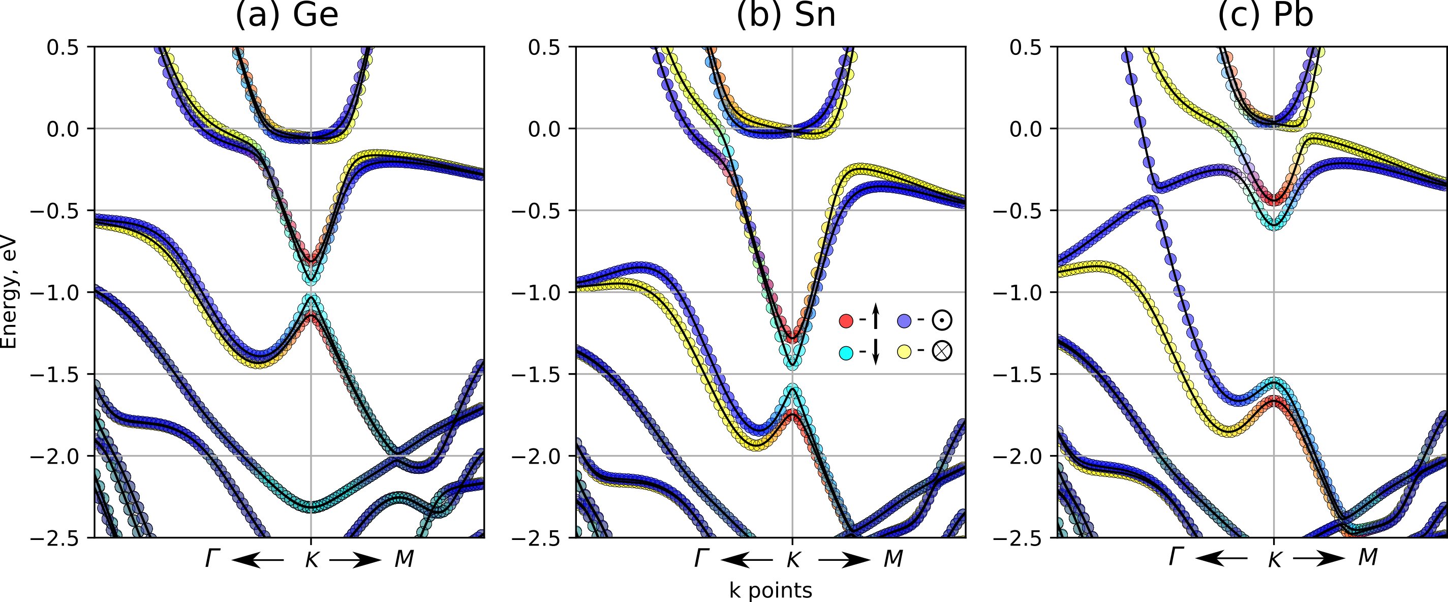
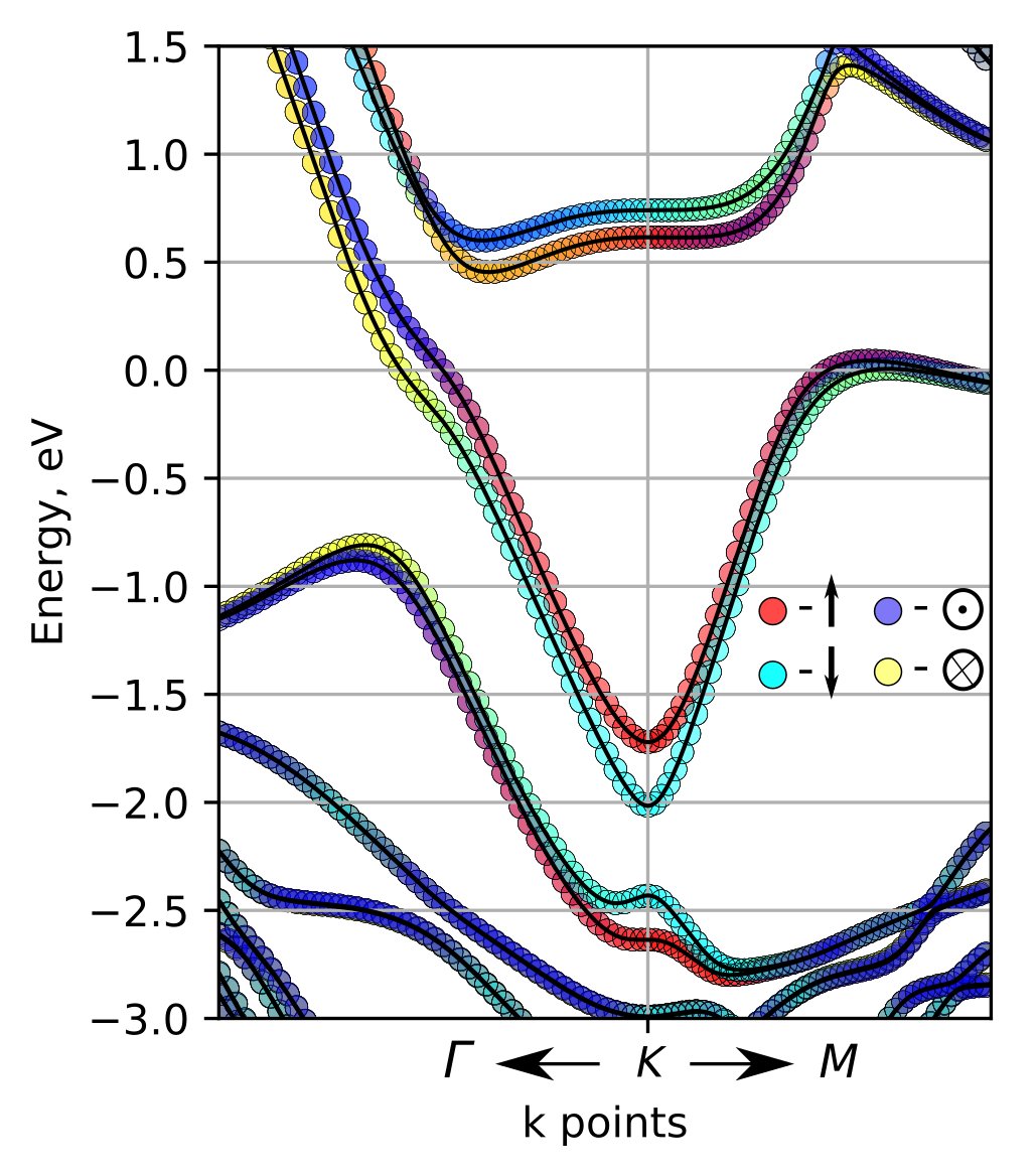
The most interesting results are obtained in calculations including SOC. The typical band structure is shown in Fig. 6 (the element specific plots could be found in Supplementarysup (Fig. S3)). The part of the band close to Fermi level shows Rashba-like spin-polarization split around and points. The calculated spin texture shows characteristic vortex like structure, shown in Fig. 6(c). It has to be noted that small normal spin component is still present in contrast with ideal classic Rashba-Bychkov effect. At the same time, Dirac-like states originating from and orbitals exhibit Zeeman-like spin-polarization with primarily normal spin components and vanishing in-plane component close to the same and points (Fig. 6(b, d)) with substantial of 120, 170, and 160 meV for Ge, Sn and Pb cases respectively.
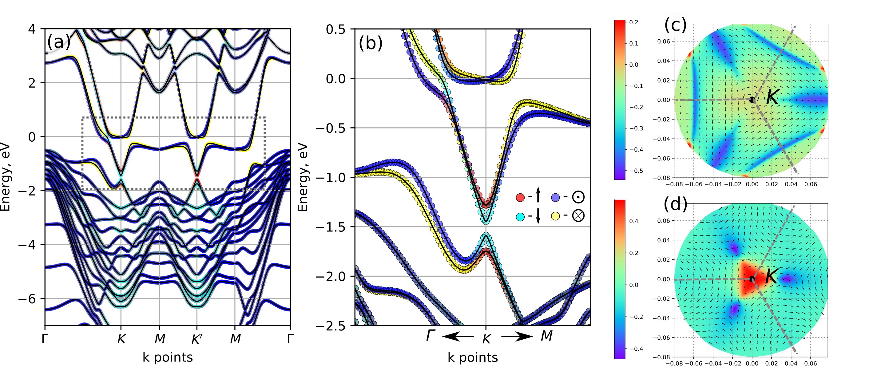

These results look very unusual. and points are non-TRIM points of the Brillouin zone, so no classic Rashba effect is expected. It has been shown, however, that in triangular systems with atomic symmetry (such as Si(111)--Bi) the local symmetry at points is (Fig. 7(e)) and in-plane, vortex-like spin-polarization is possible and has formalism similar to Rashba effect (hence called unconventional Rashba effect)Sakamoto et al. (2009b); Oguchi and Shishidou (2009). In systems with symmetry, like Si(111)--Tl, the local symmetry at points is just (Fig. 7(d, f)) and in-plane spin components are forbidden. However, surface normal component exists owing to normal effective magnetic field due to atomic character of wavefunctions and their average non-zero angular momentum, resulting in Zeeman-like spin polarizationSakamoto et al. (2009a); Nakajin and Murakami (2015). In our case, the total atomic system symmetry is , but still, at the vicinity of point, the both effects are observed simultaneously for different bands. Interestingly, the calculation of the same triangular layers residing on site produce a gap in split-band crossing point at and Zeeman-like polarization also for states, similar to reported Si(111)--Tl caseSakamoto et al. (2009a) (see Supplementarysup Fig. S4). Hence, the optimal calculated site position of our TLAL on SiC(0001) must play a crucial role in creating a Rashba-like band splitting near Fermi level. Our suggestion is that not the symmetry of atomic structure exclusively, but the symmetry of partial electron density of electronic states play an important role in the type of spin-polarization observed near special points of the Brillouin zone at least at phenomenological viewpoint. The ideal triangular layer itself possesses symmetry, which results in local symmetry at points (Fig. 7(e)). Hence, the unconventional Rashba-type state splitting should be observed in the case of inversion symmetry breaking. Indeed, if we model the single side hydrogenated TLAL layer (system which retains symmetry) we may see the Rashba splitting in SOC calculation of the related states, while there are neither Rashba nor Zeeman spin-splitting in states at points (see Supplementary Fig. S5(c)). The partial charge density of all states is also symmetric because there are no symmetry breaking perturbations (Fig. S5(a)). However, if we model the TLAL layer on SiC bilayer, even at relatively large interlayer distances of Å the perturbation of substrate with lower symmetry is enough to rearrange partial electronic density of states to those shown in Fig. 7(a) with symmetry (Fig. S5(b)). The reason for that is metastable nature of states in high symmetry environment. As there are six nearest neighbors and just three electrons to share per atom. The configuration with lower symmetry, however, creates 3-fold symmetric partial electron density much better suitable for group IV atoms. The details of such symmetry transformation is beyond the scope of the present paper and will require deep theoretical investigation. Hence, state has symmetry and symmetry at point (Fig. 7(d)). Inclusion of SOC leads to Zeeman-like splitting of these states. This phenomena would be universal for bands of TLAL on 3-fold symmetric substrate independent on the adsorption site. On the other hand, the states originating from orbital on SiC substrate couple with topmost Si dangling bonds. The degree of such coupling and prevailing character of symmetry of the resultant electron density determine which type of splitting will prevail. In the case of triangular layer adsorption on site, each orbital of metal atom will form -bond with three nearest Si dangling bonds, resulting in prevailing symmetry of the mixed state (Fig. 7(c)). So, the Zeeman-type spin-splitting is observed at points (see Supplementarysup Fig. S4). It has to be noted that some character or Rashba-effect is still persis (so-called Rashba-Zeeman subband feature, proposed previously for Rashba materials in the external normal magnetic field)Tang et al. (2015); Santander-Syro et al. (2014), as one can see that the minima of parabolic bands are still shifted in k-space from points (this may be also the reason of the flattening of the bottoms of parabolic bands at points observed in Si(111)--Tl systemSakamoto et al. (2009a)). In the case of adsorption, the orbital of metal atoms are sitting directly on top of Si dangling bonds. This configuration conserves symmetry of partial charge density to a high degree (Fig. 7(b)), and, as a result, Rashba-like splitting is still prevail, with band crossing (or a negligibly small gap) at points. We have to note also, that existence of both Rashba- and Zeeman-type splittings have been observed experimentally by spin angle-resolved photoemission spectroscopy for Sn TLAL at graphene/SiC(0001) interfaceYaji et al. .
IV Conclusions
In conclusion, we have investigated by means of DFT calculations the possibility of formation dense triangular overlayer of Ge, Sn, or Pb on SiC(0001) surface and its electronic structure. We have found that for Ge and Sn simple structure with adsorbate atom at position is stable in the adsorbate rich conditions. For Pb, due to the larger atomic radius, the buckled structure is stable and has periodicity which, however, does not reflect much on electronic properties. The band structure of TLAL exhibits characteristic cone-like feature at points below the Fermi level originating mainly from orbitals of adsorbate atom. These bands show Zeeman-like spin-splitting upon inclusion of SOC into account. Another band close to Fermi level and originating primarily from orbital shows Rashba-like spin polarization and spin vortices around non-TRIM point. This different behavior of bands is attributed to different symmetry of partial electronic density and is an important insight to understand the SOC-induced mechanism of bands spin-polarization.
References
- Odobescu et al. (2017) A. B. Odobescu, A. A. Maizlakh, N. I. Fedotov, and S. V. Zaitsev-Zotov, Phys. Rev. B 95, 195151 (2017).
- Cortés et al. (2006) R. Cortés, A. Tejeda, J. Lobo, C. Didiot, B. Kierren, D. Malterre, E. G. Michel, and A. Mascaraque, Phys. Rev. Lett. 96, 126103 (2006).
- Profeta and Tosatti (2007) G. Profeta and E. Tosatti, Phys. Rev. Lett. 98, 086401 (2007).
- Lee et al. (2013) J.-H. Lee, H.-J. Kim, and J.-H. Cho, Phys. Rev. Lett. 111, 106403 (2013).
- Badrtdinov et al. (2016) D. I. Badrtdinov, S. A. Nikolaev, M. I. Katsnelson, and V. V. Mazurenko, Phys. Rev. B 94, 224418 (2016).
- M. et al. (1996) C. J. M., H. H. Weitering, E. W. Plummer, and R. Stumpf, Nature 381, 398–400 (1996).
- Fazekas and Anderson (1974) P. Fazekas and P. W. Anderson, The Philosophical Magazine: A Journal of Theoretical Experimental and Applied Physics 30, 423 (1974).
- Li et al. (2013) G. Li, P. Höpfner, J. Schäfer, C. Blumenstein, S. Meyer, A. Bostwick, E. Rotenberg, R. Claessen, and W. Hanke, Nature Comm. 4, 1620 (2013).
- Slomski et al. (2013) B. Slomski, G. Landolt, G. Bihlmayer, J. Osterwalder, and J. H. Dil, Sci. Rep. 3 (2013), 10.1038/srep01963.
- Li et al. (2014) L. Li, S. zan Lu, J. Pan, Z. Qin, Y. qi Wang, Y. Wang, G. yu Cao, S. Du, and H.-J. Gao, Adv. Mat. 26, 4820 (2014).
- Zhang et al. (2016) L. Zhang, P. Bampoulis, A. N. Rudenko, Q. Yao, A. van Houselt, B. Poelsema, M. I. Katsnelson, and H. J. W. Zandvliet, Phys. Rev. Lett. 116, 256804 (2016).
- Xu et al. (2013) Y. Xu, B. Yan, H.-J. Zhang, J. Wang, G. Xu, P. Tang, W. Duan, and S.-C. Zhang, Phys. Rev. Lett. 111, 136804 (2013).
- Wu et al. (2014) S.-C. Wu, G. Shan, and B. Yan, Phys. Rev. Lett. 113, 256401 (2014).
- feng Zhu et al. (2015) F. feng Zhu, W. jiong Chen, Y. Xu, C. lei Gao, D. dan Guan, C. hua Liu, D. Qian, S.-C. Zhang, and J. feng Jia, Nature Mat. 14, 1020 (2015).
- Yu et al. (2017) X.-L. Yu, L. Huang, and J. Wu, Phys. Rev. B 95, 125113 (2017).
- Zhao et al. (2016) H. Zhao, C. wen Zhang, W. xiao Ji, R. wu Zhang, S. shi Li, S. shen Yan, B. min Zhang, P. Li, and P. ji Wang, Sci. Rep. 6 (2016), 10.1038/srep20152.
- Noda et al. (2003) T. Noda, S. Mizuno, J. Chung, and H. Tochihara, Jpn. J. Appl. Phys. 42, L319 (2003).
- Kim et al. (2004) N. D. Kim, C. G. Hwang, J. W. Chung, T. C. Kim, H. J. Kim, and D. Y. Noh, Phys. Rev. B 69, 195311 (2004).
- Huang et al. (1989) H. Huang, C. M. Wei, H. Li, B. P. Tonner, and S. Y. Tong, Phys. Rev. Lett. 62, 559 (1989).
- Ren et al. (2016) X.-Y. Ren, H.-J. Kim, S. Yi, Y. Jia, and J.-H. Cho, Phys. Rev. B 94, 075436 (2016).
- Brand et al. (2017) C. Brand, S. Muff, M. Fanciulli, H. Pfnür, M. C. Tringides, J. H. Dil, and C. Tegenkamp, Phys. Rev. B 96, 035432 (2017).
- Yaji et al. (2010) K. Yaji, Y. Ohtsubo, S. Hatta, H. Okuyama, K. Miyamoto, T. Okuda, A. Kimura, H. Namatame, M. Taniguchi, and T. Aruga, Nature Comm. 1, 1 (2010).
- Sakamoto et al. (2009a) K. Sakamoto, T. Oda, A. Kimura, K. Miyamoto, M. Tsujikawa, A. Imai, N. Ueno, H. Namatame, M. Taniguchi, P. E. J. Eriksson, and R. I. G. Uhrberg, Phys. Rev. Lett. 102, 096805 (2009a).
- Nakajin and Murakami (2015) K. Nakajin and S. Murakami, Phys. Rev. B 91, 245428 (2015).
- Yaji et al. (2012) K. Yaji, S. Hatta, T. Aruga, and H. Okuyama, Phys. Rev. B 86, 235317 (2012).
- Ohtsubo et al. (2011) Y. Ohtsubo, H. Muto, K. Yaji, S. Hatta, H. Okuyama, and T. Aruga, J. Phys.: Condens. Matter 23, 435001 (2011).
- Bychkov and Rashba (1984) Y. A. Bychkov and E. I. Rashba, JEPT Letters 39, 78 (1984).
- Sakamoto et al. (2009b) K. Sakamoto, H. Kakuta, K. Sugawara, K. Miyamoto, A. Kimura, T. Kuzumaki, N. Ueno, E. Annese, J. Fujii, A. Kodama, T. Shishidou, H. Namatame, M. Taniguchi, T. Sato, T. Takahashi, and T. Oguchi, Phys. Rev. Lett. 103 (2009b), 10.1103/physrevlett.103.156801.
- Hayashi et al. (2017) S. Hayashi, A. Visikovskiy, T. Kajiwara, T. Iimori, T. Shirasawa, K. Nakastuji, T. Miyamachi, S. Nakashima, K. Yaji, K. Mase, F. Komori, and S. Tanaka, Appl. Phys Express 11, 015202 (2017).
- Kresse and Furthmüller (1996) G. Kresse and J. Furthmüller, Phys. Rev. B 54, 11169 (1996).
- Blöchl (1994) P. E. Blöchl, Phys. Rev. B 50, 17953 (1994).
- Kresse and Joubert (1999) G. Kresse and D. Joubert, Phys. Rev. B 59, 1758 (1999).
- Perdew et al. (1996) J. P. Perdew, K. Burke, and M. Ernzerhof, Phys. Rev. Lett. 77, 3865 (1996).
- Reis et al. (2017) F. Reis, G. Li, L. Dudy, M. Bauernfeind, S. Glass, W. Hanke, R. Thomale, J. Schäfer, and R. Claessen, Science 357, 287 (2017).
- Petersen and Hedegård (2000) L. Petersen and P. Hedegård, Surf. Sci. 459, 49 (2000).
- (36) See Supplemental Material at [URL will be inserted by publisher].
- Medeiros et al. (2014) P. V. C. Medeiros, S. Stafström, and J. Björk, Phys. Rev. B 89, 041407 (2014).
- Oguchi and Shishidou (2009) T. Oguchi and T. Shishidou, J. Phys.: Condens. Matter 21, 092001 (2009).
- Tang et al. (2015) C.-S. Tang, S.-T. Tseng, V. Gudmundsson, and S.-J. Cheng, J. Phys.: Condens. Matter 27, 085801 (2015).
- Santander-Syro et al. (2014) A. F. Santander-Syro, F. Fortuna, C. Bareille, T. C. Rödel, G. Landolt, N. C. Plumb, J. H. Dil, and M. Radović, Nature Mat. 13, 1085 (2014).
- (41) K. Yaji, A. Visikovskiy, T. Iimori, K. Kuroda, S. Hayashi, T. Kajowara, S. Tanaka, F. Komori, and S. Shin, “Unconventional spin splitting originating from symmetry of charge density distribution,” Submitted to Phys. Rev. Lett.
Supplemental Materials: Computational study of heavy group IV elements (Ge, Sn, Pb) triangular lattice atomic layers on SiC(0001) surface
