Realizing in diamond microdisks for optomechanics via etch optimization
Abstract
Nanophotonic structures in single–crystal diamond (SCD) that simultaneously confine and co-localize photons and phonons are highly desirable for applications in quantum information science and optomechanics. Here we describe an optimized process for etching SCD microdisk structures designed for optomechanics applications. This process allows the optical quality factor, , of these devices to be enhanced by a factor of 4 over previous demonstrations to , which is sufficient to enable sideband resolved coherent cavity optomechanical experiments. Through analysis of optical loss and backscattering rates we find that remains limited by surface imperfections. We also describe a technique for altering microdisk pedestal geometry which could enable reductions in mechanical dissipation.
I Introduction
Over the past decade, advances in fabrication techniques have enabled rapid progress in the development of nanophotonic devices. This maturation is in large part thanks to researchers’ ability to borrow techniques and materials from the semiconductor electronics industry. For example, silicon-on-insulator technology, which is designed to reduce stray capacitance of electronic microchips, has provided a ready-made platform for nanophotonic optical waveguides and cavities capable of confining light to small volumes Thomson et al. (2016). In a similar spirit, nanophotonic devices have been realized in a wide variety of dielectric and semiconductor thin films, where the large refractive index contrast between a top thin film waveguide layer and the underlying substrate or removable sacrificial layer provides vertical optical confinement, while patterning of the top layer provides lateral optical confinement. The combination of large per-photon field intensities and low optical loss that can be realized in these devices have enabled studies of strong light–matter interactions that reveal new physical phenomena and can be harnessed for a wide range of applications ranging from sensing Krause et al. (2012); Wu et al. (2014, 2016), to nonlinear Evans and Mazur (2013); Lake et al. (2016); Hausmann et al. (2014) and quantum optics Fabre et al. (2017).
These innovations in nanophotonics have played a particularly critical role in the field of cavity optomechanics Aspelmeyer et al. (2014), in which nanofabricated devices are engineered to couple optical and mechanical resonances via optical forces. State-of-the-art cavity optomechanical systems have been fabricated from dielectric and semiconductor thin films, such as Si Eichenfield et al. (2009a); Chan et al. (2011), SiN Eichenfield et al. (2009b); Baker et al. (2012); Liu et al. (2013), SiO2 Schliesser et al. (2009); Weis et al. (2010); Park and Wang (2009); Dong et al. (2012) and III-V semiconductors such as GaAs Ding et al. (2010), InGaP Guha et al. (2017), AlGaAs Guha et al. (2017), GaP Mitchell et al. (2014), and AlN Xiong et al. (2012). Owing to the tight optical confinement possible in these thin film based structures, they can posses large optomechanical coupling , which quantifies the per-photon optical force in the cavity. In addition, by undercutting and releasing the waveguiding layer from the substrate via selective chemical etching, they can be mechanically isolated, enabling creation of suspended mechanical resonators with low mechanical dissipation. Together with low optical loss, these properties allow light to be coherently coupled to mechanical resonances of these devices, and operated in the sideband resolved regime commonly used for optomechanical coolingAspelmeyer et al. (2014). However, many desirable materials for nanophotonics and optomechanics applications are only available in bulk form, requiring new approaches for fabricating structures with the tight vertical optical confinement and mechanical isolation required by cavity optomechanics.
Single–crystal diamond (SCD) is one such material. Its large electronic bandgap ( eV) and associated wide transparency window results in low multiphoton absorption at telecommunication wavelengths, allowing operation at high optical power levels not supported by smaller bandgap materials such as Si. Among large bandgap materials, diamond has a moderately high refractive index (), allowing for strong optical confinement, as well as excellent mechanical and thermal properties, e.g. a Young’s modulus and thermal conductivity that are the highest among known materials. Together, these attributes make diamond attractive for nanophotonics and optomechanics applications. Furthermore, diamond is host to quantum emitters such as the nitrogen vacancy (NV) and silicon vacancy (SiV) colour centres Aharonovich et al. (2011); Schröder et al. (2016) that can be can be coupled to mechanical Teissier et al. (2014); Ovartchaiyapong et al. (2014); Lee et al. (2016); Meesala et al. (2016, 2018) and optical Englund et al. (2010); Barclay et al. (2011); Faraon et al. (2011); Riedrich-Möller et al. (2014) resonators, and used to generate single photons for quantum networking applications Sipahigil et al. (2014); Hensen et al. (2015); Sipahigil et al. (2016) and store quantum information Balasubramanian et al. (2009); Bar-Gill et al. (2013); Sukachev et al. (2017).
SCD is not currently commercially available in hetero-epitaxially grown thin film form, and although efforts to grow high quality diamond films on substrates such as Ir/MgO Washiyama et al. (2011), Ir/YSZ/Si Gsell et al. (2004); Fischer et al. (2008), and SiC/SiYaita et al. (2015) are underway, this material is not yet readily available. Integrated optical and optomechanical devices have been demonstrated in polycrystalline diamond (PCD)Wang et al. (2007); Rath et al. (2013a, b), which is commercially available in thin film form but is not an ideal host for highly coherent quantum emitters. Most state-of-the-state studies of highly coherent SiV and NV colour centres Balasubramanian et al. (2009); Chu et al. (2014); Evans et al. (2016) are performed using “bulk” SCD chips grown using chemical vapour deposition. As such, several alternative approaches to fabrication of SCD nanophotonic devices from this material have been investigated.
Efforts to create nanophotonic devices from SCD include wafer bonding and polishing Hausmann et al. (2014); Faraon et al. (2011); Lee et al. (2012); Tao et al. (2013); Bayn et al. (2014), liftoff Lee et al. (2012); Piracha et al. (2016), and use of hybrid materials Barclay et al. (2011); Riedrich-Moller et al. (2012). An arguably simpler approach is to fabricate devices directly from bulk diamond chips. This offers the possibility of creating devices from the highest quality material without requiring any manual processing steps such as bonding or polishing. To this end, ion–beam milling Babinec et al. (2011); Hiscocks et al. (2008); Atikian et al. (2017), angled plasma etching Burek et al. (2012, 2014, 2016), and plasma undercutting Khanaliloo et al. (2015a) approaches have been successful in fabricating nanophotonic structures from SCD. Of these, the quasi-isotropic plasma undercutting technique developed by Khanaliloo et al.Khanaliloo et al. (2015a) for fabricating microdisk structures from bulk diamond is unique in its ability to harness etching along diamond crystal planes in both vertical and lateral directions. It has been used to realize diamond devices with a desirable combination of high optical and small mode volume Khanaliloo et al. (2015a) and for the first demonstrations of optomechanics in SCD Khanaliloo et al. (2015b); Mitchell et al. (2016).
Recently, a modified version of the undercut process used for early demonstrations of SCD cavity optomechanical microdisks Mitchell et al. (2016) was used to create devices whose increase in , together with improvements in their thermal properties, enabled coherent coupling between light and mechanical motion, ie. optomechanically induced transparency and coolingLake et al. (2018). In the work presented in this article, we provide a detailed description of this modified fabrication process, and describe additional optimization of the etching parameters that further increases by compared to results reported in Ref. Lake et al. (2018). This places the devices in the resolved sideband regime which is a requirement for observing efficient radiation-pressure dynamical back-action effectsKippenberg and Vahala (2008); Aspelmeyer et al. (2014), such as ground state coolingChan et al. (2011), and efficient optomechanical wavelength conversionHill et al. (2012); Liu et al. (2013), which we have recently demonstrated Mitchell et al. (2018). In addition, by analyzing the influence of the microdisk’s diameter on the loss and internal scattering rates of the microdisk modes, we reveal that is likely limited by surface roughness, indicating that further improvements may be possible.
II Process overview
The approach reported here for fabricating undercut devices from bulk SCD is inspired by the SCREAM process developed for bulk single–crystal silicon MEMS microfabrication Shaw et al. (1994), and has been used by our group to fabricate nanophotonic devices such as nanobeams Khanaliloo et al. (2015b) and microdisk whispering gallery mode resonators Khanaliloo et al. (2015a). This process has seen adoption by researchers fabricating a variety of nanoscale structures from SCD Mouradian et al. (2017); Wan et al. (2018); Kiss et al. (2018), and the properties of the quasi-isotropic etch and its interaction with the diamond crystal planes have been investigated in detail in Ref. Ling et al. (2018).
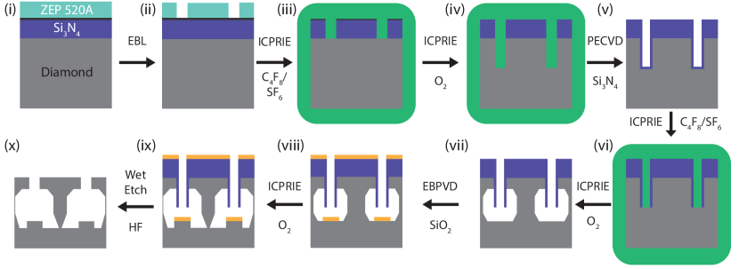
The modified process used in Ref. Lake et al. (2018) for fabricating improved microdisk optomechanical cavities is shown in Fig. 1, where the optimized steps that are the focus of this article have been highlighted in green. We start with 3 mm 3 mm optical grade, CVD grown, SCD chips purchased from Element SixIsberg et al. (2002); Balmer et al. (2009). These are mechanically polished further by Delaware Diamond Knives to surface roughness 5 nm RMS, and are cleaned in boiling piranha (150 mL H2SO4:50 mL H2O2) followed by a 3 30s rinse in H2O, and drying with N2. As an O2 inductively coupled reactive ion etch (ICPRIE) is used for all of the diamond etching steps it is necessary to use a hard mask for patterning. We have chosen Si3N4 in order to take advantage of highly optimized Si etching recipes during later steps. A 300 nm thick Si3N4 layer is deposited via plasma enhanced chemical vapor deposition (PECVD). The Si3N4 is then coated with a thin Ti layer (5 - 10 nm), deposited via electron–beam physical vapor deposition (EBPVD), which reduces charging that can be problematic during subsequent electron beam lithography (EBL) steps due to diamond’s insulating properties. Finally, a 400 nm layer of ZEP 520A is spin coated on the surface of the chip (4000 RPM, 60 s, 180C bake for 5 min while semi–covered by reflective lid). Patterning of the ZEP was performed using a Raith 150-TWO system, with beam energy of 30 keV, aperture of 10 m, and dose factor of C/cm2, followed by development for 20 s in a bath of ZED–N50, followed by IPA, both cooled to C. The ZEP pattern is then transferred to the Si3N4 hard mask layer via ICPRIE with C4F8/SF6 chemistry using an Oxford PlasmaPro 100 Estrelas Deep Silicon Etching system. This step is vital for ensuring smooth sidewalls of the diamond structures and is discussed in Sec. III. The pattern is then transferred to the diamond layer via a nearly vertical anisotropic O2 ICPRIE etch, the optimization of which is discussed in Sec. IV.
Before the undercut step, a sidewall protection layer is required to prevent unwanted etching of the patterned device. In this work a 150 nm thick conformal layer of PECVD Si3N4 was used, however, atomic layer deposited Al2O3 has also been successfully employed by Mouradian et al.Mouradian et al. (2017). This layer is then removed only from the top surface and bottom of the etch wells using the same hard mask etch chemistry and conditions as in the patterning step, which preferentially etches horizontal surfaces. The devices are then undercut via a zero bias O2 quasi-isotropic etch performed at an elevated temperature (C) to reduce the etching time required for sufficient undercutting Mitchell et al. (2016). In recent work an additional SiO2 electron beam evaporation step was added to alter microdisk pedestal profiles, as depicted in Fig. 1(viii-ix) which led to improved thermal handling, and is discussed in Sec. IV. Finally after sufficient undercutting the hard mask is stripped in 49% HF solution (20 mL), and cleaned in boiling piranha, where each acid step is followed by a 3 30 second rinse in H2O and drying with N2. Further post–processing surface treatments are discussed in Sec. V.
III Hard Mask & Sidewall Protection Layer Etch Optimization
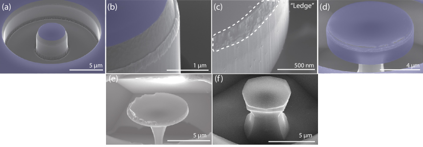
While EBL offers ultra–high resolution nano–lithography, it is vital to make the initial hard mask etch as smooth as possible to reap these benefits. Major limiting factors for of previously studied diamond microdisk structures were sidewall roughness and a “ledge” on the top edge of the microdisk Mitchell et al. (2016); Lake et al. (2018). Both of these imperfections were caused by a non-ideal hard mask etch that impacted the quality of the subsequent vertical diamond etched surfaces.
Fig. 2(a-c) illustrates the importance of the hard mask etch on the diamond sidewall roughness. The ledge seen in Fig. 2(c) was a result of breakthrough of the Si3N4 hard mask’s angled sidewalls during the anisotropic diamond etch, as seen in Fig. 2(d). It was also found that this ledge caused breakthrough of the sidewall protection layer during the quasi–isotropic plasma undercutting step (Fig. 1(vii)). Prior to the etch optimization described below, this breakthrough severely limited the yield of the process. In extreme cases it resulted in complete delamination of the sidewall protection layer, and subsequent unwanted etching of the device surfaces, as shown in Fig. 2(e,f).
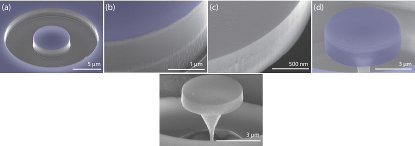
The hard mask etch was optimized following a procedure similar to HillHill (2013), by performing the identical EBL process described above on nm thick Si3N4 deposited on Si substrates. This was stopped when the Si3N4 sidewalls were smooth and close to vertical, ensuring that there was no breakthrough during the anisotropic diamond etch as shown in Fig. 3(a-c). The optimized ICPRIE etch parameters are given in Table 1. Here the ICP column refers to the power applied to the coil responsible for generating the plasma, hence controlling the ion density, while the RF column refers to the power applied to the coil responsible for accelerating the ions towards the substrate, controlling ion energy. In optimizing this etch the temperature (15∘C) and pressure (10 mTorr) were held constant. Initially tests were performed to find a bounding region for the bias voltage, which is a measure of the potential difference between the plasma and substrate electrode, achieved by varying the ICP and RF power and C4F8:SF6 gas ratio. Several iterations were performed holding either the gas ratio or RF and ICP powers constant, while varying the other. The etch quality was analyzed for varying bias voltage and gas ratio until an acceptable etch was achieved, where etch quality was determined by analyzing SEM images post–etching. Overall ratios of C4F8:SF6 from 3.75 to 0.56, ICP powers from 650 – 1800 W, and RF powers from 10–25 W were explored.
| T | Pressure | RF | Bias | ICP | C4F8 | SF6 |
| [∘C] | [mTorr] | [W] | [V] | [W] | [sccm] | [sccm] |
| 15 | 10 | 20 | 50 | 1200 | 14 | 14 |
IV Anisotropic Diamond Etch Optimization
A smooth vertical diamond etch is also critical for realizing devices with low optical loss. To this end, following the Si3N4 hard mask etch optimization, the anisotropic diamond etching process was optimized to reduce micromasking effects that can lead to rough device sidewalls Madou (2011). This optimization is also important for future devices such as photonic crystals, whose sensitivity to roughness is enhanced owing to their large surface area to volume ratio, and whose optical design is simplified if vertical sidewalls are achievable.
The anisotropic SCD etches were performed using an Oxford PlasmaPro 100 Cobra ICP system (step (iv) in Fig. 1), where the goal of this optimization was to create as smooth of diamond sidewalls as possible to reduce optical loss due to surface roughness Borselli et al. (2005). During this optimization the temperature (15∘C), chamber pressure (10 mTorr), and O2 flow rate (30 sccm) of the etches were held constant. Initially a sweep of the etcher RF power from 20 – 100 W was performed, with the ICP power held constant at 850 W. These etch conditions are labeled RF– in Table 2, and SEM images of the resulting etched devices are shown in Fig. 4. From this sweep it is apparent that low RF power results in highly angled sidewalls and slower etch rates, while the high forward RF power induces some roughness at the bases of the sidewalls. The sidewall angle as a function of DC–bias is shown in Fig. 6(a), where a maximum angle of 16∘ was observed. The etch rate was found to vary less dramatically throughout this sweep, as shown in Fig. 6(b). Note that roughness in the surrounding etch window walls present in some of these etches is a result of non–ideal EBL and is not a consequence of the individual diamond etch conditions.
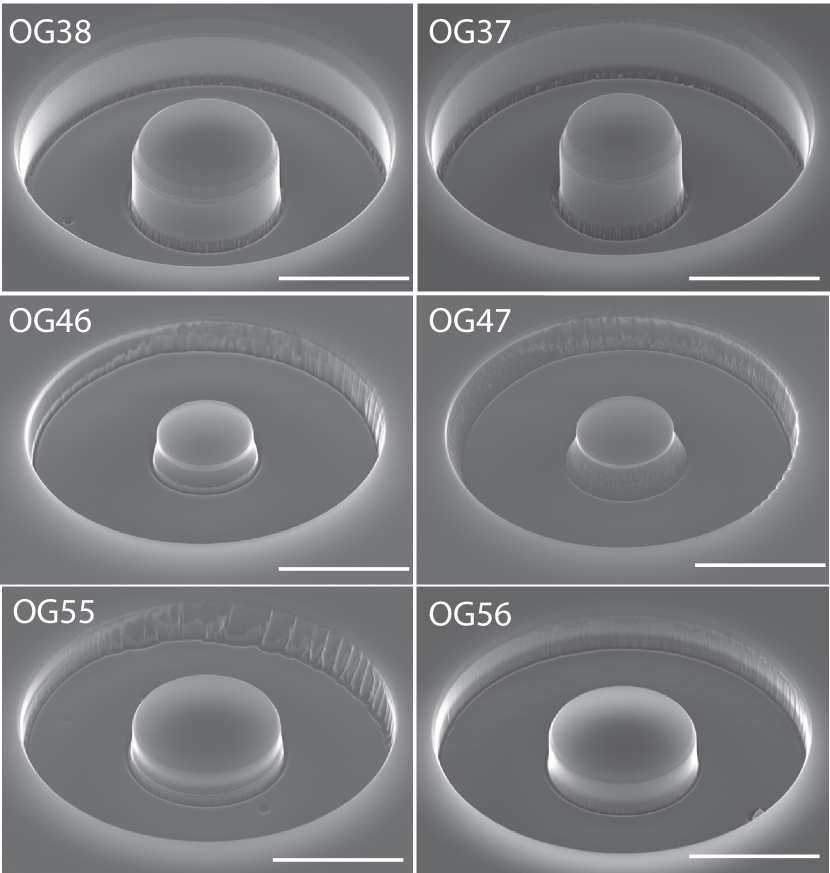
The smoothest etch, identified to be the OG36 conditions as determined by scanning electron microscope (SEM) images, was then used as a starting point for an ICP power sweep. During this sweep the DC–bias was kept roughly constant by adjusting the RF power to compensate for variations caused by the changing ICP power. This sweep is labeled “ICP” in Table 2, and SEM images of its results are shown in Fig. 5. Based on this sweep, an ICP power of 1000 W was determined to provide the best combination of sidewall smoothness and verticality. This ICP value was used for a final RF sweep, labeled “RF– in Table 2. Its results are shown in Fig. 4, from which the parameters used for sample OG56 were identified as the optimized combination of etch verticality and sidewall smoothness, and were used in the fabrication of the sample whose optical properties are characterized in the following Sec. V.
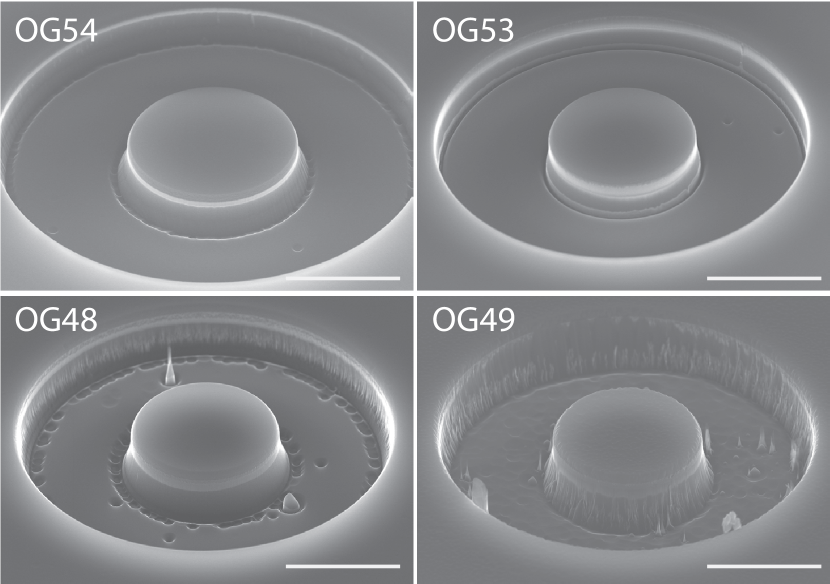

| Sample | ICP [W] | RF [W] | Bias [V] | Etch Rate [nm/s] | Sidewall Angle [∘] | Parameter Sweep |
| OG47 | 850 | 20 | 130 | 1.534 | 15.55 | RF– |
| OG46 | 850 | 40 | 190 | 1.636 | 6.509 | |
| OG38 | 850 | 60 | 230 | 1.911 | 2.976 | |
| OG36 | 850 | 80 | 279 | 1.620 | 1.107 | |
| OG37 | 850 | 100 | 311 | 1.759 | 0.636 | |
| OG54 | 850 | 80 | 281 | 2.206 | 13.27 | ICP |
| OG53 | 1000 | 90 | 286 | 2.454 | 4.063 | |
| OG48 | 1150 | 100 | 291 | 3.225 | 6.952 | |
| OG49 | 1300 | 110 | 293 | 4.062 | 8.994 | |
| OG55 | 1000 | 100 | 304 | 2.685 | 3.242 | RF– |
| OG56 | 1000 | 110 | 319 | 2.378 | 2.634 |
V Optical Characterization and Surface Treatments
Although the evaluation of the various etch conditions presented above is somewhat qualitative, a more quantitative evaluation is possible by measuring the optical properties of a fully fabricated microdisk. This requires further processing steps (vii) – (x) in Fig. 1 in order to undercut the device, as described in Sec. II. Step (vii) has already been characterized in Ref. Khanaliloo et al. (2015a) and provides a smooth bottom surface for the undercut microdisk structure, vital to observe high- optical resonances. The pedestal shaping steps (viii) and (ix) are optional, and are described in Sec. VI below. In step (x), after stripping the mask layers the sample was cleaned in heated piranha. During this step the sample was placed in H2SO4 ( mL), heated to 70∘C before adding H2O2 (2 mL), which raised the temperature of the resulting piranha solution to C. After 1 hour the sample was removed and rinsed in H2O (3 30 s) and dried with N2.
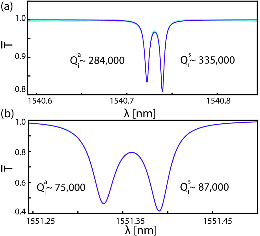
The optimized devices were evaluated by measuring of their optical modes and comparing with of un-optimized devices. Measurements were carried out by coupling a tunable diode laser (Newport TLB-6700B) to the device via a dimpled optical fiber taper, as outlined in Khanaliloo et al. (2015a); Mitchell et al. (2016); Lake et al. (2018). All measurements were performed in a N2 purged environment. Fig. 7 compares the fiber taper transmission spectrum for the highest- optical mode observed in a optimized fabrication process microdisk (Fig. 7(a)), with that of the highest- device from earlier work Lake et al. (2018) (Fig. 7(b)), demonstrating a improvement in “intrinsic” quality factor, , to . The confidence interval obtained when fitting the optical lineshape to extract is typically of and is omitted in the following analysis and figures as it would not be resolved. In this work 67 of 154 pre– and 88 of 161 post-optimization devices were initially studied as only a subset of the patterned devices are had a sufficiently small pedestal after the undercut to support high– modes, as described in Ref. Khanaliloo et al. (2015a). From this set only devices possessing a doublet structure, as shown in Fig. 7, were used in our analysis, which corresponds to 62 pre– and 68 post–optimization devices. This corresponded to the highest–Q modes () of each device, the measurements of which are presented in Figs. 8-9. Note that the vast majority of singlet modes observed did not exceed this doublet– cutoff. A small handful of singlet modes with ’s up to were observed, but are omitted from this study. The doublet nature of these modes is created by backscattering that couples the microdisk’s nominally degenerate clockwise and counterclockwise traveling wave whispering gallery modes to create standing waves Kippenberg et al. (2002); Borselli et al. (2005). Each standing wave mode is a symmetric or anti-symmetric superposition of the traveling wave modes, and they can have different and respectively, as their intensity profiles sense different volumes of the microdisk.
In general, multiple mechanisms contribute to the total optical loss rate of the microdisks, which scales as . Since loss rates are additive, we can write . The intrinsic can be decomposed as , where , , , and relate to radiation loss via leakage into unbound modes, bulk absorption, surface scattering, and surface absorption, respectively. Etch smoothness impacts , while etch chemistry and other processing that influences the diamond surface can impact . is determined by the bulk optical properties of the material, and is defined by solutions to Maxwell’s equations for modes of a device fabricated without any imperfections. Loss related to coupling with the fiber taper is accounted for the “external” .
The dominant source of loss can be identified through theoretical calculations or experimental measurements. For typical fiber taper coupling in these devices, is extracted from the fit to the optical resonance. Note that “parasitic” loss introduced by the fiber into modes not involved in input or output coupling can also be accounted for as in Spillane et al.Spillane et al. (2003), and was found to be small compared to . Bulk loss for a weakly absorbing media can be approximated by , where the wavenumber where and are the frequency and phase velocity of the light, respectively. Here is the absorption coefficient of the bulk, where and are the real and imaginary parts of the refractive index Asano et al. (2006); Xu et al. (2007); Kreuzer et al. (2008). Using cm-1 for the absorption coefficient of CVD–SCD at IR wavelengths Mildren and Rabeau (2013), results in an estimated . The radiation loss limited contribution was estimated via finite–difference time–domain simulationsOskooi et al. (2010) and found to be for the disk geometry (thickness, radius and pedestal size) studied here.
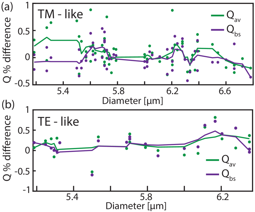
To investigate loss due to surface absorption, the pre-optimized devices were subjected to tri–acid cleaning. This 1:1:1 sulfuric, perchloric, nitric acid bath is typically used to remove graphitic surfaces detrimental to spin coherence properties of diamond nitrogen vacancy (NV) and silicon vacancy (SiV) centers Chu et al. (2014); Evans et al. (2016). It was performed using 10 mL of the acid mixture at C for 1 hr using a reflux system to capture the acid vapor, followed by rinsing in H2O (3 30 s) and drying with N2. To assess the impact of this cleaning, microdisk modes of the devices were measured before and after cleaning. These results are summarized in Fig. 8, which shows the change in measured doublet , defined as the average of and , for a range devices with varying diameter. This is quantified as “ difference”, defined as for both and , for before and after cleaning. No change in consistent across many devices or with a clear trend as a function of microdisk diameter is observed. This holds for both TE and TM like mode, whose fields are most strongly concentrated near the vertical and horizontal microdisk surfaces, respectively Borselli et al. (2005). Additionally, no significant change in the thermal capacity of the devices was observed, as determined by measuring the shift in doublet center wavelength, , as a function of dropped optical power, . This suggests that loss due to surface absorption is not limiting , provided the surface is not contaminated by material impervious to the tri-acid clean, or to the hydrofluoric acid and piranha cleaning carried out post-fabrication (see Fig. 1). Also shown in Fig. 8 is a measure of the backscattering rate, , where is the doublet splittingBorselli et al. (2005). This was also found to be unaffected by the tri-acid, suggesting that any surface roughness responsible for the mode coupling is likely related to etched diamond surface morphology, which is expected to be unaffected by the cleaning steps used here.
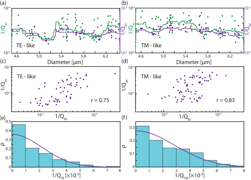
To gain additional insight into the mechanism limiting , the dependence of and on diameter for the optimized devices is plotted in Figs. 9(a) and 9(b). Although variations in and of an order of magnitude are observed, no clear dependence on diameter is noted, and we attribute the variability to imperfections unique to each microdisk, and to differences in modal radial and vertical quantum number of the modes used in the data set. However, as shown qualitatively in Figs. 9(a) and 9(b), we observe that tracks changes in as a function of diameter. This is shown more quantitatively in Figs. 9(c) and 9(d), which show scatter plots of as a function for the TE and TM modes, respectively. We find that and have a correlation coefficient, and for the TM– and TE–like modes, respectively. This correlation suggests that surface roughness is limiting . Additionally, as shown by the 1/Q histogram in Figs. 9(e,f), the density () of high- TE–like modes (Fig. 9(e)) in these microdisks is larger than that of the TM–like modes (9(f)). This suggests that there is a greater degree of surface roughness and scattering for the TM–like modes. The probability densities of for the TE– and TM– like modes in Fig. 9(e) and 9(f) were well fit to a half–normal or folded normal distribution expected for limited by surface roughness that varies randomly along the perimeter of the microdisk, with different random distribution for each disk. Finally, no large asymmetry between and of the standing wave modes was observed for any of the devices measured in this study, further supporting the conclusion that the dominant form of surface roughness limiting is distributed along the perimeter of the microdisk. This is in contrast to the effect of large discrete local perturbations along the microdisk perimeter, which can couple differently to the phase shifted spatial intensity profiles of the standing wave modes Borselli et al. (2005).
Based on the evaluation of each loss mechanism described above we conclude that is limiting , most likely due to remaining etch roughness in the anisotropic diamond etch and roughness on the top or bottom surfaces. This suggests that further improvements to could be achieved by developing a smoother anisotropic diamond etch.
VI Thermal Engineering via Pedestal Shape
When confining light to a small mode volume in a solid state structure both linear and nonlinear absorption of light can cause significant heating of the cavity Carmon et al. (2004); Barclay et al. (2005). This heating can cause instability in the cavity resonance frequency due to the thermo–optic effect and make it practically difficult to maintain a constant–cavity detuning, which is vital in many optomechanical processes. In previous work it was found that the nm diameter pedestal size of the microdisk structure pictured in Fig. 10(a) was limiting the thermal time constant of the device due to the reduced thermal conductivity in the pedestal Mitchell et al. (2016).
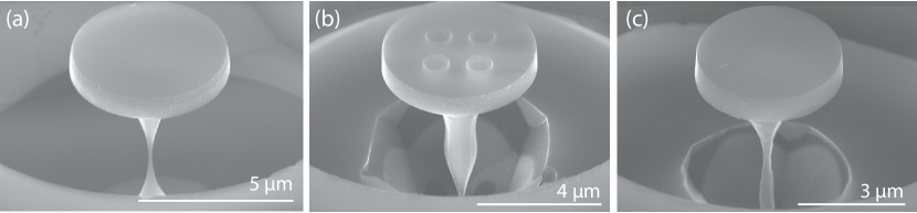
To attempt to alleviate this issue a method for altering the pedestal shape was investigated. Namely by depositing an additional masking layer it is possible to tailor the pedestal shape of the microdisk during the undercut stage. It is important to use a non-conformal layer such that the undercutting process may continue horizontally as shown in Fig. 1(viii). Here EBPVD was used to deposit a 100 nm layer of SiO2, in a line of sight fashion, allowing undercutting to continue immediately after. Here a Johnson Ultravac load-locked electron beam evaporation system was used with a deposition pressure of Torr, and a deposition rate of 0.5 Å/s. By varying the point at which this deposition occurs during the undercut the pedestal shape can be altered differently as shown in Figs. 10(a–c). Here the SiO2 was deposited after 4 hours of undercutting for the structures in Figs. 10(b,c), where an additional 4 and 5 hours were required to undercut each device respectively. This corresponds to 45% and 40% of the total undercut time, where the discrepancy in time is due to different etch depths during the anisotropic etchKhanaliloo et al. (2015a). This process can be repeated to customize the pedestal shape and could potentially be used to engineer the phononic properties of the structure, similar to the work of Nguyen et al.Nguyen et al. (2015). By altering the pedestal geometry, the device in Fig. 10(b) demonstrated an order of magnitude decrease in the thermal time constant of the microdisk structures, measured by fitting the response of the optical transmission for an input optical step function. This alteration resulted in the ability to support roughly an order of magnitude larger intracavity photon number before the onset of thermal instability Lake et al. (2018). The ability to operate at large while avoiding thermal instability is practically important in cavity optomechanics applications due to the linear dependance of the optomechanical cooperativity on , where is the single–photon coupling rate, , and Aspelmeyer et al. (2014). This enabled the observation of optomechanically induced transparency and optomechanically mediated wavelength conversion with in previously reported workLake et al. (2018); Mitchell et al. (2018).
VII Discussion
The detailed description of the fabrication process provided here will enable researchers to create a wide range of diamond photonic devices for applications including quantum photonics, nonlinear optics, and optomechanics. The optimization presented here, resulting in a increase in average for TE–like modes compared to our previous cavity optomechanical devices, was carried out over a timescale of 3 months on equipment shared with other researchers for a wide variety of processes and materials. As etch parameters vary from tool to tool, we hope that the optimization results presented here could be utilized by others to identify similar issues or devices characteristics and use our procedure to improve overall etch quality. For reference, Table 3 compares this result with the current state of the art for SCD cavities at telecommunications wavelengths. While SCD optomechanical crystals, demonstrated by Burek et al.Burek et al. (2016) provide superior , microdisks have an advantage in that they naturally support optical modes across the entire transparency window of the material, enabling multimode optomechanical experiments such as optomechanical wavelength conversionHill et al. (2012); Liu et al. (2013); Mitchell et al. (2018), and for larger microdisk diameter can have much greater radiation loss limited optical . The improvement demonstrated here is particularly meaningful for applications in cavity optomechanics, as it places the optimized devices in the resolved sideband regime where the mechanical resonance frequency, GHz for the microdisks studied here, exceeds the cavity optical energy decay rate, GHz for the high– device Aspelmeyer et al. (2014). This regime is a requirement for observing efficient radiation-pressure dynamical back-action effectsKippenberg and Vahala (2008); Aspelmeyer et al. (2014), such as ground state coolingChan et al. (2011), and low–noise amplification Ockeloen-Korppi et al. (2016). Further enhancement in optical could be achieved by improving the etch quality, and reducing surface roughness that is still present, as we conclude from the analysis above that the optical remains limited by surface imperfections. For example, incorporation of Cl2 based etching may enable smoother diamond surfaces Lee et al. (2008). Additional cleaning steps such as post–fabrication oxygen annealing, as utilized by Burek et al.Burek et al. (2016), or investigating appropriate surface termination techniques such as those devoped for siliconBorselli et al. (2006) could also be investigated for improving optical . Finally, while current SCD microdisks mechanical quality factors, , are limited by clamping loss Mitchell et al. (2016); Lake et al. (2018), the pedestal shaping step described in Sec. VI could be utilized to reduce mechanical dissipation and increase , by incorporating a phononic shield into the pedestal as demonstrated by Nguyen et al. in GaAs microdisks Nguyen et al. (2015).
| Author/Reference | Structure | Optomechanics | |
|---|---|---|---|
| This work | Microdisk | 3.35 | Yes |
| Lake et al. Lake et al. (2018) | Microdisk | 0.87 | Yes |
| Mitchell et al. Mitchell et al. (2016) | Microdisk | 0.68 | Yes |
| Khanaliloo et al. Khanaliloo et al. (2015a) | Microdisk | 1.02 | No |
| Burek et al. Burek et al. (2014) | Racetrack | 2.70 | No |
| Burek et al. Burek et al. (2016) | OMC | 3.02 | Yes |
| Teodoro et al. Graziosi et al. (2018) | Microdisk | 0.057 | No |
VIII Acknowledgements
The authors would like to thank Blaine McLaughlin for his assistance in the lab, and Ghazal Hajisalem, Aaron Hryciw, Scott Munro and Les Schowalter for all their help and support in and out of the NRC Nanotechnology Research Centre and nanoFAB.
IX Funding
This work was supported by National Research Council Canada (NRC), Alberta Innovates, National Sciences and Engineering Research Council of Canada (NSERC), and Canada Foundation for Innovation (CFI).
References
- Thomson et al. (2016) D. Thomson, A. Zilkie, J. E. Bowers, T. Komljenovic, G. T. Reed, L. Vivien, D. Marris-Morini, E. Cassan, L. Virot, J.-M. Fédéli, J.-M. Hartmann, J. H. Schmid, D.-X. Xu, F. Boeuf, P. O’Brien, G. Z. Mashanovich, and M. Nedeljkovic, Journal of Optics 18, 073003 (2016).
- Krause et al. (2012) A. G. Krause, M. Winger, T. D. Blasius, W. Lin, and O. Painter, Nature Photon. 6, 768 (2012).
- Wu et al. (2014) M. Wu, A. C. Hryciw, C. Healey, D. P. Lake, H. Jayakumar, M. R. Freeman, J. P. Davis, and P. E. Barclay, Phys. Rev. X 4, 021052 (2014).
- Wu et al. (2016) M. Wu, N. L. Y. Wu, T. Firdous, F. Fani Sani, J. E. Losby, M. R. Freeman, and P. E. Barclay, Nature Nanotechnology 12, 127 EP (2016).
- Evans and Mazur (2013) C. C. Evans and E. Mazur, in Nano-Optics for Enhancing Light-Matter Interactions on a Molecular Scale, edited by B. Di Bartolo and J. Collins (Springer Netherlands, Dordrecht, 2013) pp. 119–176.
- Lake et al. (2016) D. P. Lake, M. Mitchell, H. Jayakumar, L. F. dos Santos, D. Curic, and P. E. Barclay, Appl. Phys. Lett. 108, 031109 (2016).
- Hausmann et al. (2014) B. J. Hausmann, I. Bulu, V. Venkataraman, P. Deotare, and M. Lončar, Nature Photon. 8, 369 (2014).
- Fabre et al. (2017) C. Fabre, V. Sandoghdar, N. Treps, and L. F. Cugilandolo, eds., Quantum Optics and Nanophotonics, Lecture Notes of the Les Houches Summer School, Vol. 101 (Oxford University Press, 2017).
- Aspelmeyer et al. (2014) M. Aspelmeyer, T. J. Kippenberg, and F. Marquardt, Rev. Mod. Phys. 86, 1391 (2014).
- Eichenfield et al. (2009a) M. Eichenfield, J. Chan, R. Camacho, K. Vahala, and O. Painter, Nature 462, 78 (2009a).
- Chan et al. (2011) J. Chan, T. P. M. Alegre, A. H. Safavi-Naeini, J. T. Hill, A. Krause, S. Groblacher, M. Aspelmeyer, and O. Painter, Nature 478, 89 (2011).
- Eichenfield et al. (2009b) M. Eichenfield, R. Camacho, J. Chan, K. J. Vahala, and O. Painter, Nature 459, 550 (2009b).
- Baker et al. (2012) C. Baker, S. Stapfner, D. Parrain, S. Ducci, G. Leo, E. M. Weig, and I. Favero, Opt. Express 20, 29076 (2012).
- Liu et al. (2013) Y. Liu, M. Davanço, V. Aksyuk, and K. Srinivasan, Phys. Rev. Lett. 110, 223603 (2013).
- Schliesser et al. (2009) A. Schliesser, O. Arcizet, R. Rivière, G. Anetsberger, and T. Kippenberg, Nature Phys. 5, 509 (2009).
- Weis et al. (2010) S. Weis, R. Rivière, S. Deléglise, E. Gavartin, O. Arcizet, A. Schliesser, and T. J. Kippenberg, Science 330, 1520 (2010).
- Park and Wang (2009) Y.-S. Park and H. Wang, Nature Phys. 5, 489 (2009).
- Dong et al. (2012) C. Dong, V. Fiore, M. C. Kuzyk, and H. Wang, Science 338, 1609 (2012).
- Ding et al. (2010) L. Ding, C. Baker, P. Senellart, A. Lemaitre, S. Ducci, G. Leo, and I. Favero, Phys. Rev. Lett. 105, 263903 (2010).
- Guha et al. (2017) B. Guha, S. Mariani, A. Lemaître, S. Combrié, G. Leo, and I. Favero, Opt. Express 25, 24639 (2017).
- Mitchell et al. (2014) M. Mitchell, A. C. Hryciw, and P. E. Barclay, Appl. Phys. Lett. 104, 141104 (2014).
- Xiong et al. (2012) C. Xiong, X. Sun, K. Y. Fong, and H. X. Tang, Appl. Phys. Lett. 100, 171111 (2012).
- Aharonovich et al. (2011) I. Aharonovich, A. D. Greentree, and S. Prawer, Nature Photon. 5, 397 (2011).
- Schröder et al. (2016) T. Schröder, S. L. Mouradian, J. Zheng, M. E. Trusheim, M. Walsh, E. H. Chen, L. Li, I. Bayn, and D. Englund, J. Opt. Soc. Am. B 33, B65 (2016).
- Teissier et al. (2014) J. Teissier, A. Barfuss, P. Appel, E. Neu, and P. Maletinsky, Phys. Rev. Lett. 113, 020503 (2014).
- Ovartchaiyapong et al. (2014) P. Ovartchaiyapong, K. W. Lee, B. A. Myers, and A. C. B. Jayich, Nat. Commun. 5, 4429 (2014).
- Lee et al. (2016) K. W. Lee, D. Lee, P. Ovartchaiyapong, J. Minguzzi, J. R. Maze, and A. C. Bleszynski Jayich, Phys. Rev. Applied 6, 034005 (2016).
- Meesala et al. (2016) S. Meesala, Y.-I. Sohn, H. A. Atikian, S. Kim, M. J. Burek, J. T. Choy, and M. Lončar, Phys. Rev. Applied 5, 034010 (2016).
- Meesala et al. (2018) S. Meesala, Y.-I. Sohn, B. Pingault, L. Shao, H. A. Atikian, J. Holzgrafe, M. Gündoğan, C. Stavrakas, A. Sipahigil, C. Chia, R. Evans, M. J. Burek, M. Zhang, L. Wu, J. L. Pacheco, J. Abraham, E. Bielejec, M. D. Lukin, M. Atatüre, and M. Lončar, Phys. Rev. B 97, 205444 (2018).
- Englund et al. (2010) D. Englund, B. Shields, K. Rivoire, F. Hatami, J. Vuckovic, H. Park, and M. D. Lukin, Nano Lett. 10, 3922 (2010).
- Barclay et al. (2011) P. E. Barclay, K. M. C. Fu, C. Santori, A. Faraon, and R. G. Beausoleil, Phys. Rev. X 1, 011007 (2011).
- Faraon et al. (2011) A. Faraon, P. E. Barclay, C. Santori, K.-M. C. Fu, and R. G. Beausoleil, Nature Photon. 5, 301 (2011).
- Riedrich-Möller et al. (2014) J. Riedrich-Möller, C. Arend, C. Pauly, F. Mücklich, M. Fischer, S. Gsell, M. Schreck, and C. Becher, Nano Letters 14, 5281 (2014).
- Sipahigil et al. (2014) A. Sipahigil, K. Jahnke, L. Rogers, T. Teraji, J. Isoya, A. Zibrov, F. Jelezko, and M. Lukin, Phys. Rev. Lett. 113, 113602 (2014).
- Hensen et al. (2015) B. Hensen, H. Bernien, A. E. Dréau, A. Reiserer, N. Kalb, M. S. Blok, J. Ruitenberg, R. F. L. Vermeulen, R. N. Schouten, C. Abellán, W. Amaya, V. Pruneri, M. W. Mitchell, M. Markham, D. J. Twitchen, D. Elkouss, S. Wehner, T. H. Taminiau, and R. Hanson, Nature 526, 682 EP (2015).
- Sipahigil et al. (2016) A. Sipahigil, R. E. Evans, D. D. Sukachev, M. J. Burek, J. Borregaard, M. K. Bhaskar, C. T. Nguyen, J. L. Pacheco, H. A. Atikian, C. Meuwly, R. M. Camacho, F. Jelezko, E. Bielejec, H. Park, M. Lončar, and M. D. Lukin, Science (2016).
- Balasubramanian et al. (2009) G. Balasubramanian, P. Neumann, D. Twitchen, M. Markham, R. Kolesov, N. Mizuochi, J. Isoya, J. Achard, J. Beck, J. Tissler, V. Jacques, P. Hemmer, F. Jelezko, and F. Wrachtrup, Nature Mater. 8, 383 (2009).
- Bar-Gill et al. (2013) N. Bar-Gill, L. Pham, A. Jarmola, D. Budker, and R. Walsworth, Nat. Commun. 4, 1743 (2013).
- Sukachev et al. (2017) D. D. Sukachev, A. Sipahigil, C. T. Nguyen, M. K. Bhaskar, R. E. Evans, F. Jelezko, and M. D. Lukin, Phys. Rev. Lett. 119, 223602 (2017).
- Washiyama et al. (2011) S. Washiyama, S. Mita, K. Suzuki, and A. Sawabe, Applied Physics Express 4, 095502 (2011).
- Gsell et al. (2004) S. Gsell, T. Bauer, J. Goldfuß, M. Schreck, and B. Stritzker, Appl. Phys. Lett. 84, 4541 (2004).
- Fischer et al. (2008) M. Fischer, S. Gsell, M. Schreck, R. Brescia, and B. Stritzker, Diamond and Related Materials 17, 1035 (2008), proceedings of Diamond 2007, the 18th European Conference on Diamond, Diamond-Like Materials, Carbon Nanotubes, Nitrides and Silicon Carbide.
- Yaita et al. (2015) J. Yaita, T. Iwasaki, M. Natal, S. E. Saddow, and M. Hatano, Japanese Journal of Applied Physics 54, 04DH13 (2015).
- Wang et al. (2007) C. F. Wang, R. Hanson, D. D. Awschalom, E. L. Hu, T. Feygelson, J. Yang, and J. E. Butler, Appl. Phys. Lett. 91, 201112 (2007).
- Rath et al. (2013a) P. Rath, N. Gruhler, S. Khasminskaya, C. Nebel, C. Wild, and W. H. P. Pernice, Opt. Express 21, 11031 (2013a).
- Rath et al. (2013b) P. Rath, S. Khasminskaya, C. Nebel, C. Wild, and W. H. Pernice, Nat. Commun. 4, 1690 (2013b).
- Chu et al. (2014) Y. Chu, N. de Leon, B. Shields, B. Hausmann, R. Evans, E. Togan, M. J. Burek, M. Markham, A. Stacey, A. Zibrov, A. Yacoby, D. Twitchen, M. Loncar, H. Park, P. Maletinsky, and M. Lukin, Nano Lett. 14, 1982 (2014).
- Evans et al. (2016) R. E. Evans, A. Sipahigil, D. D. Sukachev, A. S. Zibrov, and M. D. Lukin, Phys. Rev. Applied 5, 044010 (2016).
- Lee et al. (2012) J. C. Lee, I. Aharonovich, A. P. Magyar, F. Rol, and E. L. Hu, 20, 8891 (2012).
- Tao et al. (2013) Y. Tao, J. M. Boss, B. A. Moores, and C. L. Degen, Nat. Commun. 5, 3638 (2013).
- Bayn et al. (2014) I. Bayn, S. Mouradian, L. Li, J. A. Goldstein, T. Schroder, J. Zheng, E. H. Chen, O. Gaathon, M. Lu, A. Stein, C. A. Ruggiero, J. Salzman, R. Kalish, and D. Englund, Appl. Phys. Lett. 105, 211101 (2014).
- Piracha et al. (2016) A. H. Piracha, P. Rath, K. Ganesan, S. Kühn, W. H. P. Pernice, and S. Prawer, Nano Letters 16, 3341 (2016), pMID: 27111636.
- Riedrich-Moller et al. (2012) J. Riedrich-Moller, L. Kipfstuhl, C. Hepp, E. Neu, C. Pauly, F. Mucklich, A. Baur, M. Wandt, S. Wolff, M. Fischer, S. Gsell, M. Schreck, and C. Becher, Nature Nanotech. 7, 69 (2012).
- Babinec et al. (2011) T. M. Babinec, J. T. Choy, K. J. M. Smith, M. Khan, and M. Lončar, Journal of Vacuum Science & Technology B 29, 010601 (2011).
- Hiscocks et al. (2008) M. Hiscocks, K. Ganesan, B. Gibson, S. Huntington, F. Ladouceur, and S. Prawer, Opt. Express 16, 19512 (2008).
- Atikian et al. (2017) H. A. Atikian, P. Latawiec, M. J. Burek, Y.-I. Sohn, S. Meesala, N. Gravel, A. B. Kouki, and M. Loncar, APL Photonics 2, 051301 (2017).
- Burek et al. (2012) M. J. Burek, N. P. de Leon, B. J. Shields, B. J. Hausmann, Y. Chu, Q. Quan, A. S. Zibrov, H. Park, M. D. Lukin, and M. Lončar, Nano Lett. 12, 6084 (2012).
- Burek et al. (2014) M. J. Burek, Y. Chu, M. S. Z. Liddy, P. Patel, J. Rochman, S. Meesala, W. Hong, Q. Quan, M. D. Lukin, and M. Lončar, Nat. Commun. 5, 5718 (2014).
- Burek et al. (2016) M. J. Burek, J. D. Cohen, S. M. Meenehan, N. El-Sawah, C. Chia, T. Ruelle, S. Meesala, J. Rochman, H. A. Atikian, M. Markham, D. J. Twitchen, M. D. Lukin, O. Painter, and M. Lončar, Optica 3, 1404 (2016).
- Khanaliloo et al. (2015a) B. Khanaliloo, M. Mitchell, A. C. Hryciw, and P. E. Barclay, Nano Lett. 15, 5131 (2015a).
- Khanaliloo et al. (2015b) B. Khanaliloo, H. Jayakumar, A. C. Hryciw, D. P. Lake, H. Kaviani, and P. E. Barclay, Phys. Rev. X 5, 041051 (2015b).
- Mitchell et al. (2016) M. Mitchell, B. Khanaliloo, D. P. Lake, T. Masuda, J. P. Hadden, and P. E. Barclay, Optica 3, 963 (2016).
- Lake et al. (2018) D. P. Lake, M. Mitchell, Y. Kamaliddin, and P. E. Barclay, ACS Photonics 5, 782 (2018).
- Kippenberg and Vahala (2008) T. Kippenberg and K. Vahala, Science 321, 1172 (2008).
- Hill et al. (2012) J. T. Hill, A. H. Safavi-Naeini, J. Chan, and O. Painter, Nat. Commun. 3, 1196 (2012).
- Mitchell et al. (2018) M. Mitchell, D. P. Lake, and P. E. Barclay, in Conference on Lasers and Electro-Optics (Optical Society of America, 2018) p. SF2J.1.
- Shaw et al. (1994) K. A. Shaw, Z. Zhang, and N. C. MacDonald, Sensors and Actuators A: Physical 40, 63 (1994).
- Mouradian et al. (2017) S. Mouradian, N. H. Wan, T. Schroder, and D. Englund, Appl. Phys. Lett. 111, 021103 (2017).
- Wan et al. (2018) N. H. Wan, S. Mouradian, and D. Englund, Applied Physics Letters 112, 141102 (2018).
- Kiss et al. (2018) M. Kiss, T. Graziosi, and N. Quack, in Proc. SPIE, Vol. 10513 (2018).
- Ling et al. (2018) X. Ling, Z. T. X., S. R. J., and Y. Amir, Advanced Materials 30, 1705501 (2018).
- Isberg et al. (2002) J. Isberg, J. Hammersberg, E. Johansson, T. Wikström, D. J. Twitchen, A. J. Whitehead, S. E. Coe, and G. A. Scarsbrook, Science 297, 1670 (2002).
- Balmer et al. (2009) R. S. Balmer, J. R. Brandon, S. L. Clewes, H. K. Dhillon, J. M. Dodson, I. Friel, P. N. Inglis, T. D. Madgwick, M. L. Markham, T. P. Mollart, N. Perkins, G. A. Scarsbrook, D. J. Twitchen, A. J. Whitehead, J. J. Wilman, and S. M. Woollard, Journal of Physics: Condensed Matter 21, 364221 (2009).
- Hill (2013) J. T. Hill, Nonlinear Optics and Wavelength Translation Via Cavity-Optomechanics, Ph.D. thesis, Caltech (2013).
- Madou (2011) M. J. Madou, Fundamentals of Microfabrication and Nanotechnology, 3rd ed., Vol. 2 (CRC Press, 2011).
- Borselli et al. (2005) M. Borselli, T. J. Johnson, and O. Painter, Opt. Express 13, 1515 (2005).
- Kippenberg et al. (2002) T. J. Kippenberg, S. M. Spillane, and K. J. Vahala, Opt. Lett. 27, 1669 (2002).
- Spillane et al. (2003) S. M. Spillane, T. J. Kippenberg, O. J. Painter, and K. J. Vahala, Phys. Rev. Lett. 91, 043902 (2003).
- Asano et al. (2006) T. Asano, B.-S. Song, and S. Noda, Opt. Express 14, 1996 (2006).
- Xu et al. (2007) T. Xu, S. Yang, S. V. Nair, and H. E. Ruda, Phys. Rev. B 75, 125104 (2007).
- Kreuzer et al. (2008) C. Kreuzer, J. Riedrich-Möller, E. Neu, and C. Becher, Opt. Express 16, 1632 (2008).
- Mildren and Rabeau (2013) R. P. Mildren and J. R. Rabeau, eds., Optical Engineering of Diamond (Wiley-VCH Verlag & Co. KGaA, 2013).
- Oskooi et al. (2010) A. F. Oskooi, D. Roundy, M. Ibanescu, P. Bermel, J. Joannopoulos, and S. G. Johnson, Comp. Phys. Comm. 181, 687 (2010).
- Carmon et al. (2004) T. Carmon, L. Yang, and K. J. Vahala, Opt. Express 12, 4742 (2004).
- Barclay et al. (2005) P. E. Barclay, K. Srinivasan, and O. Painter, Opt. Express 13, 801 (2005).
- Nguyen et al. (2015) D. T. Nguyen, W. Hease, C. Baker, E. Gil-Santos, P. Senellart, A. Lemaître, S. Ducci, G. Leo, and I. Favero, New J. Phys. 17, 023016 (2015).
- Ockeloen-Korppi et al. (2016) C. F. Ockeloen-Korppi, E. Damskägg, J.-M. Pirkkalainen, T. T. Heikkilä, F. Massel, and M. A. Sillanpää, Phys. Rev. X 6, 041024 (2016).
- Lee et al. (2008) C. Lee, E. Gu, M. Dawson, I. Friel, and G. Scarsbrook, Diamond and Related Materials 17, 1292 (2008), proceedings of Diamond 2007, the 18th European Conference on Diamond, Diamond-Like Materials, Carbon Nanotubes, Nitrides and Silicon Carbide.
- Borselli et al. (2006) M. Borselli, T. J. Johnson, and O. Painter, Appl. Phys. Lett. 88, 131114 (2006).
- Graziosi et al. (2018) T. Graziosi, S. Mi, M. Kiss, and N. Quack, APL Photonics 3, 126101 (2018).