Negative photoconductivity and hot-carrier bolometric detection of terahertz radiation in graphene-phosphorene hybrid structures
Abstract
We consider the effect of terahertz (THz) radiation on the conductivity of the ungated and gated graphene (G)-phosphorene (P) hybrid structures and propose and evaluated the hot-carrier uncooled bolometric photodetectors based on the GP-lateral diodes (GP-LDs) and GP-field-effect transistors (GP-FETs) with the GP channel. The operation of the GP-LDs and GP-FET photodetectors is associated with the carrier heating by the incident radiation absorbed in the G-layer due to the intraband transitions. The carrier heating leads to the relocation of a significant fraction of the carriers into the P-layer. Due to a relatively low mobility of the carriers in the P-layer, their main role is associated with a substantial reinforcement of the scattering of the carriers. The GP-FET bolometric photodetector characteristics are effectively controlled by the gate voltage. A strong negative conductivity of the GP-channel can provide much higher responsivity of the THz hot-carriers GP-LD and GP-FET bolometric photodetectors in comparison with the bolometers with solely the G-channels.
I Introduction
Unique energy spectra, of graphene (G) 1 and a few-layer Black Phosphorus layer or phosphorene (P) 2 , their optical and electric properties, and recent advances in technology open remarkable prospects for the creation of novel devices using G-layers 3 ; 4 ; 5 ; 6 , the P-layers 2 ; 7 ; 8 ; 9 ; 10 , and different hybrid structures including the G-P hybrid structures 11 ; 12 ; 13 . In particular, the GP hybrid systems can be used for the improvement of various devices. The possibility of the layer-dependent alignment work function control 2 ; 14 provides substantial flexibility in the device design. In this paper, we propose and evaluate the detector of the terahertz (THz) radiation based on a lateral diode (LD) and a field-effect transistor (FET) with the GP channel, GP-LD and GP-FET, respectively. The operation of the GP-LD and GP-FET photodetectors with the GP-channel is associated with the carrier heating by the incident radiation absorbed in the G-layer leading to a variation of the channel conductivity 15 ; 16 . This principle is used in the hot-carrier bolometers based on the G-channel exhibiting the negative or positive photoconductivity (see, for example 17 ; 18 ; 19 ; 20 ; 21 and references therein). However, a major disadvantage of using G-layers in the bolometric photodetectors is that the conductivity of pristine G-layers is weakly dependent on the carrier temperature. This can be overcome by the introduction of the barrier regions (by partitioning of the channel into nanoribbons in which the energy gap is opened 17 or using disordered G-layers 20 ). In the G-P bolometers under consideration, the carrier heating caused by the absorbed radiation leads to the transfer of a significant portion of the carriers into the P-layer. This results in a decrease of the density of the highly mobile carriers in the G-layer and in a reinforcement of the scattering of these carriers on the carriers residing in the P-layer. Due to a high effective mass of the carriers in the P-layer and, hence, a relatively low mobility, their main role is associated with a substantial reinforcement of the scattering of the carriers in the G-layer. As a result, the conductivity of the GP-channel can markedly drop with the carrier heating. We demonstrate that the effect of the negative THz photoconductivity in the G-P channels can be much stronger than that for the G-channels, particularly at room temperature. Therefore, the GP-LDs and GP-FETs could effectively operate as the uncooled hot-carrier THz bolometers with an elevated responsivity.
II Model
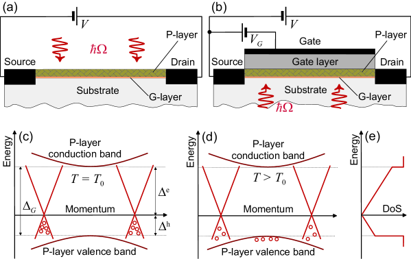
Figure 1 demonstrates a schematic view of the ungated and gated G-P structures (i.e., a GP-LD and a GP-FET with the GP-channels). It is assumed that the P-layer consisting of a few atomic layers, is oriented in such a way that the direction from the source to its drain corresponds to the zigzag direction. The dynamics of electrons and holes in this direction is characterized by a huge effective mass. As a result, a substantial amount of the electrons and holes can relocate from the G-layer (where their mobility could be very high) to the P-layer (with a low mobility).
For the sake of definiteness, we consider the P-layer consisting of several atomic P-layers (), assuming that in both GP-LD and GP-FET structures it is p-doped (the pristine P-layers are of p-type). At the incident THz photon energies , where is the Fermi energy of the main carriers (holes), the carrier heating is associated with its interband (Drude) absorption in the G-layer.
The band gap and the energy spacing and , between the Dirac point in the G-layer and the edges of the conduction and valence bands, (determined by the pertinent work functions) depend on the number . In the G-P channel under consideration (with or 5), the band structure is asymmetric: 14 .
The dispersion relation for the holes in the G- and P-layers can be presented as
| (1) |
| (2) |
respectively. Here cm/s is the characteristic velocity of electrons in the G-layers, and are the components of the effective mass tensor (), and are the carrier momenta in the source-drain direction and the perpendicular direction, respectively. The components of the effective mass tensor for the valence bands () are approximately equal to and , where is the mass of a free electron.
The model under consideration is based on the following assumptions:
(1) The sufficiently frequent electron-electron, electron-hole, and hole-hole collisions enable the establishment of the distinct quasi-Fermi electron and hole distributions with the common effective temperature in both G- and P-layers and split quasi-Fermi levels due to the carrier-phonon interband scattering. This is consistent with the numerous experimental studies in which the G-layer was excited with an optical or infrared pump pulse and probed with photoelectron or optical spectroscopy at different photon energies (see, for example, 18 and the references therein). Sufficiently strong interactions between the electrons and holes belonging to both G- and P-layers promote the inter-layer equilibrium 22 ; 23 ; 24 . Hence, the electron and hole distribution functions are the following functions of the carrier energy : (where and are the quasi-Fermi energies counted from the Dirac point).
(2) Due to heavy electron and hole effective masses and ,
the conductivity of the P-layer is relatively small because this layer mobility in the direction corresponding to the mass is proportional to 25 , so that
the P-layer conductivity could be neglected in comparison with
the G-layer conductivity. Thus, the main role of the carrier relocation from the G-layer into the P-layer
is associated with an intensification of the carriers (in the G-layer) scattering on the carriers (in the P-layer) when the concentration of the latter increases with the carrier system heating.
(3) The momentum relaxation of the electrons and holes in the G-layer (which we refer to as the ”light” electrons and holes) is due to their scattering on acoustic phonons, neutral defects, and heavy particles in the P-layer. In contrast to the G-channel-based THz bolometers intended for the operation at very low temperatures at which the carrier energy relaxation is due to the interaction with acoustic phonons, the energy relaxation in the uncooled bolometric detectors under consideration is associated with the optical phonons in the G-layer. The interband transitions assisted by the optical phonons 26 ; 27 and with the Auger processes (see 28 ; 29 and the discussion therein)are assumed to be the main recombination-generation mechanisms. We characterize the relative role of these processes by the parameter , where and are the times characterizing the pertinent interband transitions (we call this parameter as the Auger parameter). When , the quasi-Fermi energies can be markedly different ().
III Conductivity of the G-P-channel
The net surface charge density in the GP-channel, which comprises the electron and hole charges in both the G- and P-layers, induced by the acceptors and the gate voltage is equal to (where , which is proportional to the acceptor density, corresponds to the charge neutrality point, and are the background dielectric constant and the thickness of the gate layer, and is the electron charge). By introducing the voltage (gate) swing , we unify the consideration of the GP-LDs and GP-FETs. In particular, the case of GP-LDs corresponds to , so that , while in the GP-FETs can be both negative and positive.
The gate voltage swing or its dimensional value and the quantities , , and are related to each other as
| (3) |
Here is the Fermi-Dirac integral 30 , , , , and is the Planck constant. For and therefore setting , ( and ), nm and , and meV ( K), one can obtain and V. A large value of is due to a relatively high density of states in the P-layer.
In equilibrium at sufficiently low temperatures, when the P-layer is empty (the second term in the right-hand side of Eq. (3) is negligible), Eq. (3) yields when is relatively large.
When the electron-hole system in the G-P channel is heated by the source-to-drain DC voltage or by the incident radiation, the electron and hole quasi-Fermi levels can be split: . Accounting for the competition between the optical phonon mediated and the Auger generation-recombination processes, the equation governing the carrier interband balance can result in the following equation relating and at an arbitrary effective temperature :
| (4) |
where is the optical phonon energy. Equation (4) generalizes that obtained previously 13 for the case of the dominant optical phonon generation-recombination processes by the introduction of a phenomenological factor .
Considering Eq. (4), we rewrite Eq. (3) as
| (5) |
In particular, using Eq. (5), one can obtain immediately the dependence of the hole Fermi energy on the voltage swing .
Focusing on the GP-channels with dominant carrier scattering on acoustic phonons, neutral defects, on each other, and on the short-range screened heavy carriers, the momentum relaxation time as a function of the carrier momentum can be set as , where is the momentum relaxation time in the G-layer with the effective scatterer density at and is the net scatterer density, which accounts for the density, , of the heavy carriers in the P-layer. In this case, the GP-channel conductivity could be presented as (in line with 15 ; 16 ; 31 ; 32 ; 33 ; 34 ; 35 ; 36 ):
| (6) |
with being the G-layer low electric-field conductivity. Using Eqs. (4) and (6), the GP-channel conductivity can be expressed via the G-layer conductivity (without the P-layer conductivity) with the latter expressed via the effective temperature and the hole quasi-Fermi energy :
| (7) |
| (8) |
The density of scatterers (heavy holes), , in the P-layer, which exponentially increases with increasing and , can also be expressed via these quantities:
| (9) |
where . The factor in the latter formula reflects the fact that the density of states in the few-layer P-layer increases with the layer number 15 .
The second factor in the right-hand side of Eq. (6) reflects an increase in the scatterer density associated with the inclusion of the scattering on the heavy holes in the P-layer. It is instructive that at when , the G-channel conductivity is independent of . This is because of the specific of the carrier scattering in the system under consideration (scattering on acoustic phonons, neutral defects and effectively screened charged scatterers) 35 ; 36 ; 37 ; 38 .
Using Eqs. (7) - (9), we obtain
| (10) |
Equations (5) and (10) describe the dependences of the quasi-Fermi energy and the G-P-channel conductivity on the effective temperature and the voltage swing . Solving these equations, one can obtain the characteristics of the GP-channel in wide ranges of the normalized voltage swing , carrier effective temperature , and the density .
IV Negative photoconductivity in the G-P channels
The variation of the current density, , in the GP-channel for small effective carrier temperature variations is given by
| (11) |
where is the linear density of the source-drain dc current in the absence of the irradiation (i.e., the dark current density, and are the source-drain electric field and voltage, respectively, is the length of the GP-channel, and is given by Eq. (10). An increase in the carrier effective temperature (the carrier heating) caused by the irradiation corresponds to the negative photoconductivity temperature when the conductivity derivative . The latter is in line with the experimental observations 18 ; 19 ; 37 ; 38 . Figure 2 shows and (i.e., with ) found as functions of using Eqs. (5) and (10) for different values of the scatterer density in the G-layer. One can see from Fig. 2 that both the quantities and are negative. Here and in the following, we assume that meV, meV, cm-2, cm-2 corresponding to ps, , meV ( 300K), and . The scatterer densities range cm-2 at meV, corresponds to the rather practical values of the carrier mobility in G-layers cm2/s V 39 ; 40 ; 41 ; 42 .
At small , the absolute values of these quantities . However, at sufficiently large , can be substantially larger than , particularly, at . This is attributed to a steeper effective temperature dependence of the GP-channel conductivity due to an increasing hole population in the P-layer. The latter implies that the GP-channel can exhibit a stronger temperature dependence and, hence, a stronger effect of the negative photoconductivity than the G-channel. The comparison of the plots in Figs. 2(a) – 2(c) demonstrates that the relative intensification of the Auger processes (a decrease in the parameter ) leads to a marked decrease in , diminishing the temperature dependence of the G-channel, while these processes weakly affect the temperature dependence of the GP-channel and, hence, the quantities and .
V Responsivity of the GP-photodetectors
We limit our following consideration by the GP photodetectors operating as hot-carrier bolometers, so that the incident radiation does not produce a marked amount of the extra electrons and holes and the variation of the carrier density is associated primarily with the heating processes. This happens when is sufficiently large (to provide large hole Fermi energy ), the photon energy is not too large (). and the carrier momentum relaxation time is not too short, so that the intraband absorption dominates the interband absorption (see Appendix A).
Under irradiation, the carrier effective temperature varies. Its value can be found considering the balance of the power, , receiving by the carriers due to the absorption of the incident radiation with the photon energy and the power, , which the carriers transfer to the lattice. As assumed above, the latter is associated with the interband transitions accompanied by the emission and absorption of the G-channel optical phonons having the energy . The power received by the carrier system is given by
| (12) |
where is the speed of light, is the radiation photon flux, is the high-frequency G-P channel conductivity, is the average hole momentum relaxation time in the GP-channel, which considering that , can be estimated as
| (13) |
Here . At and , Eq. (13) yields and , respectively.
Taking into account Eqs. (7), (10), and (12) at , we obtain
| (14) |
| (15) |
where is the equilibrium number of optical phonons, is the characteristic time of the spontaneous emission of optical phonons at the intraband transitions, and (at and (at are the carrier densities in the G-channel at . For simplicity, below we use the following interpolation formulas:
| (16) |
| (17) |
Equalizing and given by Eqs. (14) and (15), and taking into account Eq. (16), we arrive at the following equation which relates the variation of the carrier effective temperature and the photon flux :
| (18) |
where is the fine structure constant. The latter formula corresponds to the hole energy relaxation time . Setting ps (for example, 43 ), one obtains ps.
Taking into account the variation of the current density, , in the GP-channel caused by the irradiation, the GP bolometer intrinsic current responsivity can be presented by the following expression:
| (19) |
Here is the GP-channel area, is the channel length (the spacing between the source and the drain), and is the channel width, i.e., its size in the direction perpendicular to the current direction. Using Eqs. (11) and (18), we arrive at the following:
| (20) |
Here
| (21) |
In the above calculations we have not accounted for the carrier heating by the source-drain electric field assuming that it is weak, so that is very close to . The pertinent condition is as follows:
| (22) |
For , the quantity , given by Eq. (21), is equal to
| (23) |
At ps, ps, and cm, for the quantities and max one can find V/cm and max A/W, respectively.
The voltage responsivity , where is the load resistance. Setting equal to the GP-channel resistance, i.e., . In this case, for one obtains
| (24) |
with
| (25) |
Setting , we arrive at the following expression for the characteristic value of the GP bolometer voltage responsivity:
| (26) |
For ps, ps, and cm, we obtain V/W. Naturally, at weaker source-drain electric fields , the quantities and are smaller than max and max.
Using Eqs. (20) and (24) at relatively low frequencies , the current and voltage responsivities can be presented as
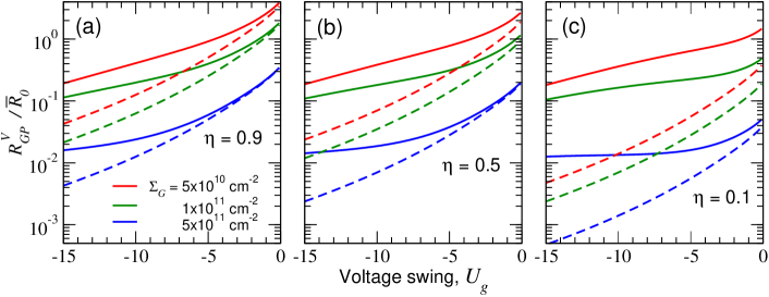
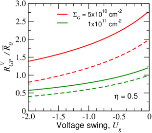
| (27) |
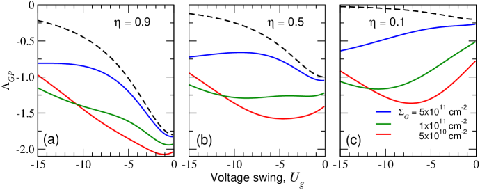
Figures 3 and 4 show the GP-bolometers voltage low-frequency responsivity normalized by the quantity as a function of the voltage swing calculated using Eqs. (10) and (27) for the same structural parameters as for Fig. 3 (given in Sec. 4). The normalized responsivity of the G-detectors (with the G-channel) is also shown by the dashed lines. First, as seen from Figs. 3 and 4, the responsivity sharply decreases with an increase in the scatterer density and the voltage swing . This is attributed to a weaker carrier heating at their stronger scattering and their larger density. The latter markedly rises with increasing . Second, the GP-bolometer responsivity, moderately exceeding that of the G-bolometer responsivity at small , becomes orders of magnitudes larger at elevated values of (compare the solid and dashed lines in Figs. 3 and 4). The difference in the GP- and G-bolometers responsivities becomes fairly pronounced at smaller Auger parameter (at stronger Auger generation-recombination processes). This correlates with a drop of clearly seen in Fig. 2.
VI Bandwidth and gain-bandwidth product
As follows from Eqs. (20) and (24), the GP-bolometer responsivity decreases when the photon frequency , where the cut-off frequency is given by
| (28) |
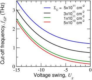
At small , Eq. (27) yields , so that for the values of used above, one obtains THz. At relatively large , the frequency can be much higher than that at . This is seen from Fig. 5, which shows the cut-off frequency as a function of the normalized voltage swing calculated using Eq. (28). The cut-off frequency is larger than the pertinent frequency for the G-bolometers by a factor . At large values of and , this factor can be larger than that at .
The comparison of the gain-bandwidth products of the GP- and G-bolometers, defined as max and , yields the following estimate for these factors ratio . As seen from Fig. 3, markedly exceeds unity, particularly at .
VII Detectivity of the GP-bolometers
The dark-current-limited detectivity of the GP-bolometers can be evaluated as (see, for example, 44 :
| (29) |
where is the net source-drain dc current
Equations (18) and (24) for relatively low frequencies yield
| (30) |
with
| (31) |
for an arbitrary , and
| (32) |
for . Using the same parameters as for the above estimates of max and assuming that cm, at , one obtains cm/W.
The GP-bolometer dark-current-limited detectivity , given by Eq. (30), exhibits a fairly steep drop with increasing resembling that of the responsivity shown in Fig. 3. One should note that the difference in the detectivities for a smaller and those corresponding to a larger is more pronounced that the pertinent difference in the responsivities.
VIII Discussion
VIII.1 General comments
As seen from Eq. (11), the quantity determines the variation of the GP-channel conductivity due to the carrier heating. Its absolute value exhibits a maximum at a certain value of , which depends on . This is seen from Fig. 3. Considering only the variation of the channel conductivity associated with the carrier transfer to the P-layer, from Eq. (10) we find for and the maximum of its modulus
| (33) |
| (34) |
respectively. This maximum is reached at . i.e., at relatively moderate population of the P-layer () that corresponds to or . For , , and cm-2, the pertinent values of are approximately equal to -6, -10, and -23, respectively. The latter is in line with plots in Fig. 2. It is interesting that max and are a linear and a quadratic functions of , respectively.
The obtained results show that the responsivity and detectivity of the GP-bolometers steeply decrease with increasing voltage swing (see Fig. 3). Thus, it is practical to use the range of relatively small , although the bandwidth of the GP-bolometers extends with increasing as seen from Fig. 5. Thus, there is an opportunity of the voltage control of the cut-off frequency. In the GP-LDs, the minimum value of is determined by the acceptor density in the GP-channel, so that this density should be minimized to achieve acceptable characteristics. Apart from easier fabrication, the GP-LDs can exhibit the enhance performance of the whole bolometric photodetector due to a more effective THz radiation input.
As demonstrated above, the characteristics of the GL-LD and GL-FET bolometers under consideration can be markedly different depending on the Auger parameter . This parameter depends on the substrate material, particularly, on its dielectric constant . The calculations 29 predicted the optical phonon recombination time in the G-layers from less than a picosecond to several picoseconds at the carrier densities under consideration above and room temperature. The experimental results of the carrier recombination dynamics in G-layer 45 were interpreted assuming that the interband relaxation is associated with the optical phonon processes rather than the carrier-carrier processes, so that (and is close to unity). The recent calculations 29 (as well as the previous one’s 46 ) showed that an increase in leads to a virtually linear increase in and, hence, in an increase in . Although, this increase in is not too pronounced - the change in from 5 to 25 results in a fourfold rise of at room temperature 29 . For example, in the case of GP-LDs with SiO2 and hBN substrates, in which , ps, whereas bin the case of the HfO2 substrate, ps. In the GP-FETs, the screening of the carrier interaction by a highly conducting gate can substantially suppress the Auger processes. Indeed, using the data obtained recently 29 , one can find that being ps at and the gate layer thickness nm, becomes ps at nm. One needs to point out that in the case of high- substrates, additional recombination channel associated with the substrate polar phonons 47 can promote father increase in . Setting ps, we find that the latter values of correspond to . Hence, the range of the Auger parameter variations assumed in the above calculations appear to be reasonable.
The values of the GP-detector responsivity demonstrated in Fig. 3 are of the same order of magnitude or can exceed the room temperature responsivity of the proposed and realized THz photodetectors based on different heterostructures 21 ; 48 ; 49 ; 50 ; 51 ; 52 ; 53 ; 54 ; 55 ; 56 ; 57 ; 58 ; 59 , including those based on the P-channel 7 ; 60 ; 61 (although in G-based devices at very low temperatures much higher responsivities have been achieved 20 ).
VIII.2 Assumptions
The main assumptions of our device model are fairly natural and practical. We disregarded the contribution of the carriers in the P-layer to the net conductivity of the G-P-channel. The pertinent condition can be presented as or where is the carrier mobility in the P-layer. Assuming that cm2/s V 60 (see also 2 ) cm-2, and meV (i.e., , see Fig. 2),the above inequalities are valid if ps. The values of assumed in our calculations well satisfy this requirement.
(i) Above we estimated the scattering time and, hence, as in 15 : , so that , where , is the characteristic potential of the scatter, and is the screening length. Setting nm or smaller (see also the estimate for at meV 13 and below), we find cm/s. At cm-2 and meV, the latter yields ps. For the scattering on the acoustic phonons due to the deformation potential interaction with the longitudinal vibrations at meV, one obtains cm/s and ps. The contribution of the hole-hole scattering in the G-layer to its dc and ac conductivity are small (despite substantially non-parabolic hole spectrum 59 ). The role of the hole-electron scattering is also small due low electron densities, particularly, at high gate voltages.
(ii) The interband absorption of the incident radiation with the photons with the energies in the G-layer disregarded in our model, is practically prohibited due to the Pauli blocking. At small values of (i.e., small ), this absorption is weak in comparison with the intraband (Drude) absorption if
| (35) |
At , inequality (31) implies ps.
(iii) Considering the features of the DoS (see Fig. 1(e)), the screening length, , of the charges in the GP-channel at low and relatively high voltage swing and is given by
| (36) |
respectively Assuming and setting meV and meV, from Eq. (32) we obtain nm. The products of the characteristic carrier wavenumbers and and the pertinent values of are and . The latter indicates a rather short range interaction (an effective screening of the charged impurities and the heavy carriers in the P-layer) in the device under consideration at its working conditions.
IX Conclusions
We studied the effect of THz photoconductivity of the G- and GP-channels and showed that their conductivity decreases under the THz irradiation (the effect of negative conductivity). It was revealed that this effect in G-channels is determined by the competition of the interband transitions associated with optical phonons and the Auger generation-recombination processes and vanishes when the latter processes prevail. However, the negative conductivity in the GP-channels is weakly sensitive to the relative roles of the latter process. The negative photoconductivity of the ungated and gated GP-channels (GP-LDs and GP-FETs) under the THz irradiation, enables using these devices as bolometric THz photodetectors. We evaluated the responsivity, bandwidth, and detectivity characteristics of such THz bolometers and demonstrated that an effective transfer of the carriers from the G-layer into the P-layer, caused by their heating due to the intraband absorption of the THz radiation, leads to the substantial decrease in the G-P-channel conductivity. This effect of the negative THz photoconductivity is associated primarily with the intensification of the light carrier scattering in the G-layer on the heavy carriers in the P-layer. Using the developed device model for the GP-LD and GP-FET bolometers, we demonstrated that these photodetectors can exhibit a fairly high responsivity in a wide range of the THz frequencies at the room temperature. The main requirement to achieve the elevated photodetector performance is having sufficiently high values of the G-layer mobility. The main characteristics of the GP-FET bolometers are effectively controlled by the gate voltage. The GP-LD and GP-FET THz bolometric photodetectors can substantially surpass the THz bolometers with the G-channel and compete and even outperform the existing devices. Further enhancement of the GP-LD and GP-FET THz bolometer can be realized using the GP-GP-…-GP superlattice heterostructures as the channel, integrating the GP-LDs and GP-FETs with THz microcavities or waveguides, and implementing different schemes of the plasmonic enhancement of the THz absorption.
Appendix A. Short-range versus long-range scattering
As seen from Fig. 2, in the G-channels the quantity . This implies that the carrier heating in the G-layers by the absorbed radiation leads to a decrease in the conductivity, i.e. to the negative photoconductivity. This phenomenon was observed in the experiments (see, for example, 18 ; 19 ; 37 ; 38 ). As shown above, the G-layer negative photoconductivity at the room temperatures can appear when the short-range scattering dominates and the Auger generation-recombination processes are weaker than those associated with the optical phonons. In the case of the dominant long-range scattering, the G-layer conductivity rises with increasing carrier effective temperature 15 . In the model 18 , the G-layer conductivity was considered assuming that is independent of carrier momentum . In such a model,
| (A1) |
At small and high ratios and , Eq. (A1) yields and , respectively. This results (accounting for Eq. (4)) in and . One can see that at , as in the case considered by us, the G-layer conductivity decreases with increasing carrier temperature. However, this effect vanishes (the conductivity becomes insensitive to the carrier temperature variation and, hence, to the irradiation) when the Auger parameter tends to zero. Thus, even in this case, the carrier temperature dependence of the GP-channel conductivity , related to according to Eq. (10), corresponds to the negative photoconductivity with the main contribution of the carrier transfer to the P-layer.
On the contrary, if the long-range scattering with would dominate, could be a rising function of the carrier temperature leading to the positive G-layer photoconductivity. This can surpass the effect of the G-to-P carrier transitions. Both types of the G-layer photoconductivity (negative and positive) depending on the photon energy and the enviromental gases have been observed, for example, in 38 .
Appendix B. Frequency dependence of the GP- and G-channel conductivity
Following the standard procedures (see, for example, 32 ), the ac conductivity can be presented as (compare with Eq. (6))
| (B1) |
At low and high frequencies frequencies, Eq. (B1) can be rewritten as
| (B2) |
| (B3) |
respectively, where
| (B4) |
For and , Eq. (B4) yields
| (B5) |
so that as a function of can, for example, be interpolated by Eq. (16). In the case of the dominating long-range scattering, for the cut-off frequency one obtains .
Acknowledgments
The authors are grateful to P. P. Maltsev, A. Satou, D. Svintsov, and V. Vyurkov for useful discussions. VR is also thankful to N. Ryabova for assistance.he work was supported by Japan Society for Promotion of Science, KAKENHI Grant No. 16H06361, the Russian Science Foundation (Grant No.14-29-00277), Russian Foundation for Basic Research (Grant No. 18-07-01145), RIEC Nation-Wide Collaborative Research Project, and by Office of Naval Research (Project Monitor Dr. Paul Maki).
References
- (1) A. H. Castro Neto, F. Guinea, N. M. R. Peres, K. S. Novoselov, and A. K. Geim, “The electronic properties of graphene,”Rev. Mod. Phys. 81 109–162(2009).
- (2) Xi Ling, H. Wang, S. Huang, F. Xia, and M. S. Dresselhaus, “The renaissance of black phosphorus,”Proc. Nat. Acad. Sci USA, 112, 4523–4530 (2015).
- (3) F. Bonaccorso, Z. Sun, T. Hasan, and A. Ferrari, “Graphene photonics and optoelectronics,”Nat. Photonics 4, 611–622 (2010).
- (4) V. Ryzhii, M. Ryzhii, V. Mitin, and T. Otsuji, “Toward the creation of terahertz graphene injection laser,”J. Appl. Phys. 110, 094503 (2011).
- (5) Q. Bao and K. P. Loh, “Graphene photonics, plasmonics, and broadband optoelectronic devices,”ACS Nano 6, 3677–3677 (2012).
- (6) A. Tredicucci and M. Vitiello, “Device concepts for graphene-based terahertz photonics,”J. Sel. Top. Quant. 20, 130–138 (2014).
- (7) M. Buscema, D. J. Groenendijk, S. I. Blanter, G. A. Steele, H. S. J. van der Zant, and A. Castellanos-Gomez, “Fast and broadband photoresponse of few-layer black phosphorus field-effect transistors,”Nano Lett. 14, 3347–3352 (2014).
- (8) M. Engel, M. Steiner, and Ph. Avouris, “A black phosphorus photo-detector for multispectral high-resolution imaging,”Nano Lett. 14, 6414–6417 (2014).
- (9) E. Leong, R. J. Suess, A. B. Sushkov, H. D. Drew, T. E. Murphy, and M. Mittendorff, “Terahertz photoresponse of black phopsporus,”Opt. Express 25, No. 11, 12666–12674 (2017).
- (10) F. Ahmed, Y. D. Kim, M. S. Choi, X. Liu, D. Qu, Z. Yang, J. Hu, I. P. Herman, J. Hone, W. J. Yoo, “High electric field carrier transport and power dissipation in multilayer black phosphorus field effect transistor with dielectric engineering,”Adv. Funct. Mater. 27, 1604025 (2017).
- (11) Y. Deng, Z. Luo, N. J. Conrad, H. Liu, Y. Gong, S. Najmaei, P. M. Ajayan, J. Lou, X. Xu, P. D. Ye, “Black phosphorus-monolayer MoS2 van der Waals heterojunction p-n diode,”ACS Nano 8, 8292–8299 (2014).
- (12) F. H. L. Koppens, T. Mueller, Ph. Avouris, A, C. Ferrari, M. S. Vitiello, and M. Polini, “Photodetectors based on graphene, other two-dimensional materials and hybrid systems,”Nat. Nanotech. 9, 780–793 (2014).
- (13) V. Ryzhii, M. Ryzhii, D. Svitsov, V. Leiman, P. P. Maltsev, D. S. Ponomarev, V. Mitin, M. S. Shur, and T. Otsuji, “Real-space-transfer mechanism of negative differential conductivity in gated graphene-phosphorene hybrid structures: Phenomenological heating model,”J. Appl. Phys. 124 (2018), in press [arXiv: 1806.06227 (2018)].
- (14) Y. Cai, G. Zhang, and Y.-W. Zhang, “Layer-dependent band alignment and work function of few-layer phosphorene,”Sci. Reports 4, 6677 (2014).
- (15) F. T. Vasko and V. Ryzhii, “Voltage and temperature dependencies of conductivity in gated graphene,”Phys. Rev. B 76, 233404 (2007).
- (16) O. G. Balev, F. T. Vasko, and V. Ryzhii, “Carrier heating in intrinsic graphene by s strong dc electric field”Phys. Rev. B79, 165432 (2009).
- (17) V. Ryzhii, T Otsuji, M. Ryzhii, N. Ryabova, S. O. Yurchenko, V. Mitin, and M. S. Shur, “Graphene terahertz uncooled bolometers,”J. Phys. D: Appl. Phys. 46, 065102 (2013).
- (18) J. N. Heyman, J. D. Stein, Z. S. Kaminski, A. R. Banman, A. M. Massari, and J. T. Robinson, “Carrier heating and negative photoconductivity in graphene,”J. Appl. Phys. 117, 015101 (2015).
- (19) Xu Du, D. E. Prober, H. Vora, and C. Mckitterick, “Graphene-based bolometers,”Graphene 2D Mater. 1, 1–22 (2014).
- (20) Qi Han, T. Gao, R. Zhang, Yi Chen, J. Chen, G. Liu, Y. Zhang, Z. Liu, X. Wu, and D. Yu, “Highly sensitive hot electron bolometer based on disordered graphene,”Sci Rep. 3, 3533 (2013).
- (21) G. Skoblin, J. Sun, and A. Yurgens, “Graphene bolometer with thermoelectric readout and capacitive coupling to an antenna,”Appl. Phys. Lett. 112, 063501 (2018)
- (22) G. Zhang, A. Chaves, S. Huang F. Wang1, Q. Xing, T. Low, and H. Yan1, “Determination of layer-dependent exciton binding energies in few-layer black phosphorus,”Sci. Advances 16 Mar 2018: Vol. 4, no. 3, eaap9977.
- (23) T. Low, R. Roldán, H. Wang, F. Xia, P. Avouris, L. M. Moreno, F. Guinea, “Plasmons and screening in monolayer and multilayer black phosphorus,”Phys. Rev. Lett. 113, 106802 (2014).
- (24) S. Yuan, A. N. Rudenko, and M. I. Katsnelson, “Transport and optical properties of single- and bilayer black phosphorus with defects,”Phys. Rev. B 91, 115436 (2015).
- (25) J. Xi, M. Long, D. Wang, and Z. Shuai, “First principles prediction of charge mobility in carbon and organic nanomaterials,”Nanoscale 4, 4348–4369 (2012).
- (26) F. Rana, P. A. George , J. H. Strait, S. Sharavaraman, M. Charasheyhar, and M. G. Spencer, “Carrier recombination and generation rates for intravalley and intervalley phonon scattering in graphene,”Phys. Rev. B 79, 115447 (2009).
- (27) V. Ryzhii, M. Ryzhii, V. Mitin, A. Satou, and T. Otsuji, “Effect of heating and cooling of photogenerated electron-hole plasma in optically pumped graphene on population inversion,”Jpn. J. Appl. Phys. 50, 094001 (2011).
- (28) M. S. Foster and I. L. Aleiner, “Slow imbalance relaxation and thermoelectric transport in graphene,”Phys. Rev. B 79, 085415 (2009).
- (29) G. Alymov, V. Vyurkov, V. Ryzhii, A. Satou, and D. Svintsov, “Auger recombination in Dirac materials: A tangle of many-body effects,”Phys. Rev. B 97, 205411 (2018).
- (30) J. S. Blakemore, Semiconductor Statistics, Dover, 1987.
- (31) T. Ando, “Screening Eefect and impurity scattering in monolayer graphene,”J. Phys, Soc. Japan 75, 074716 (2006)
- (32) L. A. Falkovsky and A. A. Varlamov, “Space-time dispersion of graphene conductivity,”European Phys. J. B 56, 281–284 (2007).
- (33) E. H. Hwang, S. Adam, and S. D. Sarma, “Carrier transport in two-dimensional graphene layers,”Phys. Rev. Lett. 98, 186806 (2007).
- (34) V. Vyurkov and V. Ryzhii, “Effect of Coulomb scattering on graphene conductivity,”JETP Lett. 88, 370–372 (2008).
- (35) E. H. Hwang and S. Das Sarma, “Acoustic phonon scattering limited carrier mobility in two-dimensional extrinsic graphene,”Phys. Rev. B 77, 115449 (2008).
- (36) E. H. Hwang and S. Das Sarma, “Screening induced temperature dependent transport in 2D graphene,”Phys. Rev. B 79, 165404 (2009).
- (37) G. Jnawali, Y. Rao, H. G. Yan, and T. F. Heinz,“Observation of a transient decrease in terahertz conductivity of single-layer graphene induced by ultrafast optical excitation,”Nano Lett. 13, 524–530 (2013).
- (38) C. J. Docherty, C. T. Lin, H. J. Joyce, R. J. Nicholas, L. M. Hertz, L. J. Li, and M. B. Johnston, “Extreme sensitivity of graphene photoconductivity to environmental gases,”Nat. Comm. 3,1228 (2012)
- (39) S. V. Morozov, K. S. Novoselov, M. I. Katsnelson, F. Schedin, D. C. Elias, J. A. Jaszczak, and A. K. Geim, “Giant intrinsic carrier mobilities in graphene and its bilayer,”Phys. Rev. Lett.100, 016602 (2008).
- (40) H. Hirai, H. Tsuchiya, Y. Kamakura, N. Mori, and M. Ogawa, “Electron mobility calculation for graphene on substrates,”J. Appl. Phys. 116, 083703 (2014).
- (41) L. Banszerus, M. Schmitz, S. Engels, J. Dauber, M. Oellers, F. Haupt, K. Watanabe, T. Taniguchi, B. Beschoten, and C. Stampfer, “Ultrahigh-mobility graphene devices from chemical vapor deposition on reusable copper,”Science Advances 1, No. 6. , e1500222 (2015).
- (42) L. Wang, I. Meric, P. Y. Huang, Q. Gao, Y. Gao, H. Tran, T. Taniguchi, K. Watanabe, L. M. Campos, D. A. Muller, J. Guo, P. Kim, J. Hone, K. L. Shepard, and C. R. Dean,“One-dimensional electrical contact to a two-dimensional material,”Science 342, 614-617 (2013).
- (43) K. J. Tielrooij, J. C.W. Song, S. A. Jensen, A. Centeno, A. Pesquaera, A. Z. Elorza, M. Bonn, L. S. Levitov, and F. H.L. Koppens, “Photoexcitation cascade and multiple hot-carrier generation in graphene,”Nat. Phys. 9, 248–252 (2013).
- (44) H. Schneider and H,C, Liu, it Quantum Well Infrared Photodetectors: Physics and Applications, Springer, NY, 2007.
- (45) J. M. Dawlaty, S. Shivaraman, M. Chandrashekhar, F. Rana, and M. G. Spencer “Measurement of ultrafast carrier dynamics in epitaxial graphene,”Appl. Phys. Lett. 92, 042116 (2008).
- (46) F. Rana, “Electron-hole generation and recombination rates for coulomb scattering in graphene, ”Phys. Rev. B 76, 155431 (2007).
- (47) F. Rana, J. H. Strait, H, Wang, and C, Manolatou, “Ultrafast carrier recombination and generation rates for plasmon emission and absorption in graphene,”Phys. Rev. B 84, 045437 (2011).
- (48) S. D. Gunapala, S. V. Bandara, J. K. Liu, J. M. Mumolo, S. B. Rafol, D. Z. Ting, A. Soibel, and C. Hill, “Quantum Well Infrared Photodetector Technology and Applications,”IEEE J. Sel. Topics Quant. Electron. 20, No. 6 (2014).
- (49) V. Ryzhii, T. Otsuji, V. E. Karasik, M.Ryzhii, V. Leiman, V. Mitin, and M. S. Shur, “Comparison of intersubband quantum-well and interband graphene layer infrared photodetectors,”IEEE J. Quant. Electron. 54, No. 2 (2018).
- (50) V. Ryzhii, M. Ryzhii, M. S. Shur, V. Mitin, A Satou, and T Otsuji, “Resonant plasmonic terahertz detection in graphene split-gate field-effect transistors with lateral p–n junctions,”J. Phys. D: Appl. Phys. 49, 315103 (2016).
- (51) M. Mittendorff, S. Winnerl, J. Kamann, J. Eroms, D. Weiss, H, Schneider1, and M. Helm, “Ultrafast graphene-based broadband THz detector,”Appl. Phys. Lett. 103, 021113 (2013).
- (52) V.Ryzhii, M.Ryzhii, D.Svintsov, V.Leiman, V.Mitin, M.S.Shur,and T .Otsuji,“Nonlinear response of infrared photodetectors based on van der Waals heterostructures with graphene layers,”Optics Express 25,5536-–5549 (2017).
- (53) . V. Ryzhii, M. Ryzhii, V. Leiman, V. Mitin, M. S. Shur, and T. Otsuji, “Effect of doping on the characteristics of infrared photodetectors based on van der Waals heterostructures with multiple graphene layers,”J. Appl.Phys. 122, 054505 (2017).
- (54) V. Ya. Aleshkin, A. A. Dubinov, S. V. Morozov, M. Ryzhii, T. Otsuji, V. Mitin, M. S. Shur, and V. Ryzhii, “Interband infrared photodetectors based on HgTe-CdHgTe quantum-well heterostructures,”Opt. Mat. Exp. 8, 1349 (2018).
- (55) V. Ryzhii, M. Ryzhii, V. Mitin, and T. Otsuji, “Terahertz and infrared photodetection using p-i-n multiple-graphene-layer structures,”J. Appl. Phys. 107, 054512 (2010).
- (56) A. V. Muraviev, S. L. Rumyantsev, G. Liu, A. A. Balandin, W. Knap, and M. S. Shur, “Plasmonic and bolometric terahertz detection by graphene field-effect transistor,”Appl. Phys. Lett. 103, 181114 (2013)
- (57) Y. Wang, W. Yin, Q. Han, X. Yang, H. Ye, Q. Lv, D. Yin, “Bolometric effect in a waveguide-integrated graphene photodetector,”Chin Phys. B 25, 118103 (2016).
- (58) D. A. Bandurin, D. Svintsov, I. Gayduchenko, S. G. Xu, A. Principi, M. Moskotin, I. Tretyakov, D. Yagodkin, S. Zhukov, T. Taniguchi, K. Watanabe, I. V. Grigorieva, M. Polini, G. Goltsman, A. K. Geim, and G. Fedorov, “Resonant terahertz detection using graphene plasmons,”arXiv: 1807.04703 (2018).
- (59) D. S. Ponomarev, D. V. Lavrukhin, A. E. Yachmenev, R. A. Khabibullin, I. E. Semenikhin, V. V. Vyurkov, M. Ryzhii, T. Otsuji, and V. Ryzhii1, “Lateral terahertz hot-electron bolometer based on an array of Sn nanothreads in GaAs,”J. Phys. D: Appl. Phys. 51, 135101 (2018).
- (60) L. Viti, J. Hu, D. Coquillat, A. Politano, W. Knap, and M. S. Vitiello, “Efficient Terahertz detection in black-phosphorus nano-transistors with selective and controllable plasma-wave, bolometric and thermoelectric response,”Scientific Reports 6, 20474 (2016).
- (61) E. Leong, R. J. Suess, A. B. Sushkov, H. D. Drew, T. E. Murphy, and M. Mittendorff, “Terahertz photoresponse of black phosphorus,”Optics Express 25, 12666–12674 (2017).
- (62) D. Svintsov, V. Ryzhii, A. Satou, T. Otsuji, and V. Vyurkov, “Carrier-carrier scattering and negative dynamic conductivity in pumped graphene,”Optics Express 22 , 19873–19886 (2014).