Rethinking Image Sensor Noise for Forensic Advantage111 Copyright 2018. This manuscript version is made available under the CC-BY-NC-ND 4.0 license http://creativecommons.org/licenses/by-nc-nd/4.0/
Abstract
Sensor pattern noise has been found to be a reliable tool for providing information relating to the provenance of an image. Conventionally sensor pattern noise is modelled as a mutual interaction of pixel non-uniformity noise and dark current. By using a wavelet denoising filter it is possible to isolate a unique signal within a sensor caused by the way the silicon reacts non-uniformly to light. This signal is often referred to as a fingerprint. To obtain the estimate of this photo response non-uniformity multiple sample images are averaged and filtered to derive a noise residue. This process and model, while useful at providing insight into an images provenance, fails to take into account additional sources of noise that are obtained during this process. These other sources of noise include digital processing artefacts collectively known as camera noise, image compression artefacts, lens artefacts, and image content. By analysing the diversity of sources of noise remaining within the noise residue, we show that further insight is possible within a unified sensor pattern noise concept which opens the field to approaches for obtaining fingerprints utilising fewer resources with comparable performance to existing methods.
keywords:
Sensor Pattern Noise , Photo Response Non-Uniformity , Digital Image Forensics , Dark Current1 Introduction
Sensor pattern noise (SPN) is a reliable tool for tracking the provenance of images [1]. Through the use of high-pass filtering, a unique signal can be extracted from an image consisting of Photo-Response non-uniformity (PRNU) noise. This signal is unique to the image sensor and is capable of discrimination across cameras of the same make and model. This discrimination is because the PRNU is defined as the pixel to pixel variance in output intensity of an image sensor when illuminated with a constant light source. The PRNU is the light-sensitive signal caused by Pixel Non-Uniformity (PNU) within a discrete image sensor. It is statistically unlikely for two image sensors to have the same PRNU fingerprint. This capability has been demonstrated with a false acceptance rate of 0.0024% and a false rejection rate of 2.4% making PRNU comparison an attractive tool where other evidence can also be used to verify the outcome [2]. The PRNU approach was further reinforced experimentally by [3] showing that a camera with a positive match to an image with the same PRNU is 1/100,000 or 99.999%.
Since images in the real world are often never illuminated with a constant light source, solving the blind source camera identification problem in this manner requires large sample sizes of images specially crafted to ensure scene contamination is minimised. Processing the large sample of images is either time consuming or requires large amounts of computing resources to ensure efficacy. These resources are not always available for forensic investigators in the field who need efficient tools to quickly and accurately quarantine evidence. There are further challenges in maintaining chain of evidence for embedded cameras, such as in contemporary smart phones and the emerging field of wearable technologies.
Through careful analysis of the current sensor technology in terms of optical effects, semiconductor physics and the environment image sensors operate in, this paper considers the current methodology for measuring the unique PRNU signal and shows that other options exist for extracting the unique signal that may provide more accurate results and lead to the development of more efficient tools.
2 Basic operation of an Image Sensor
The fundamental principle of collecting a digital image has not changed since the first experiments involving selenium-coated metal plates [4]. Since then the progression from plates to tubes [5] (realising the vision of [6]), to Charged Couple Device (CCD) arrays [7] [8] and currently to CMOS imaging sensors (CIS) [9] [10] has seen the quality of the image improve, but the principle remains the same. Photons are converted to electrons in a PN junction of a photosensitive material through the recombination of holes and electrons via the photoelectric effect. In the current state of the art pinned photodiode (PPD) conversion of photons to electrons is done in the heavily P doped layer of the PN diode. This is because the PPD architecture results in the depletion layer being almost the entire width of the P+ region [11].
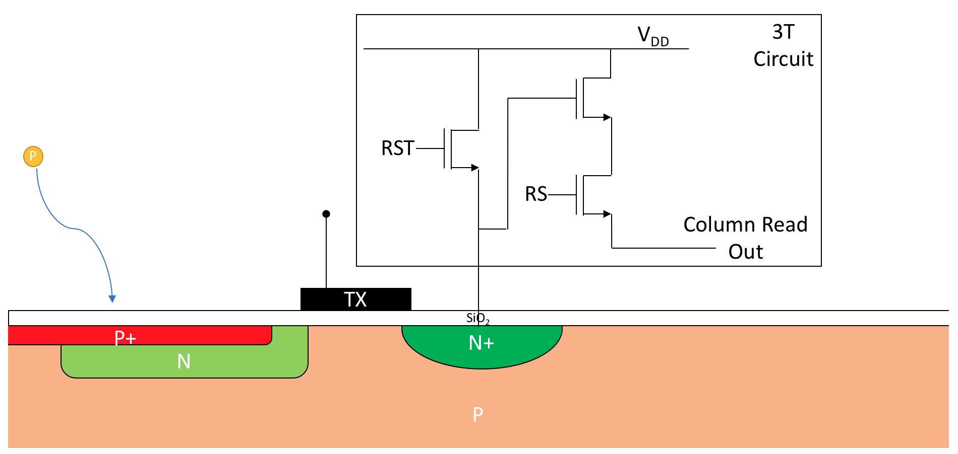
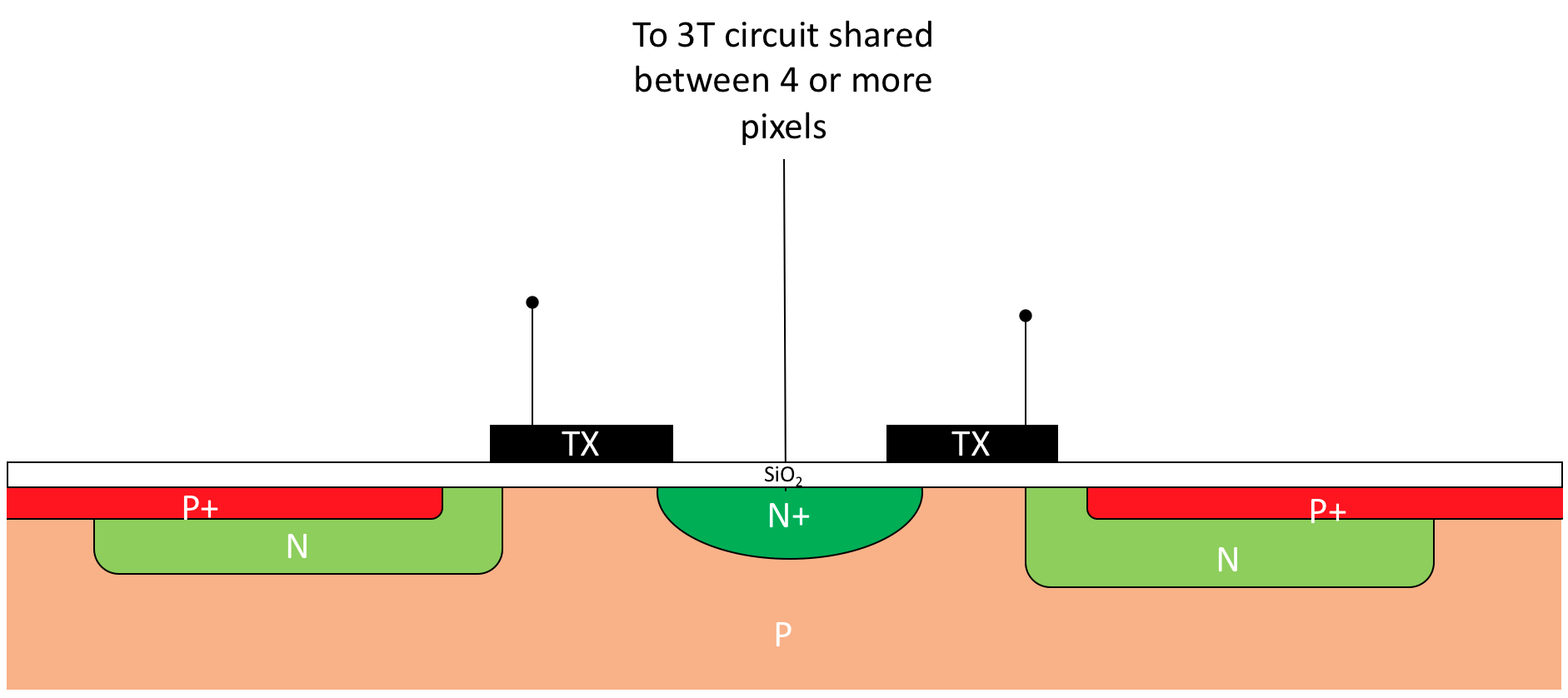
The PPD is the preferred architecture for modern CIS (Figure 1) due to several significant advantages over its predecessors [12]. The PPD exhibits lower noise, lower dark current, higher sensitivity and broader dynamic range than traditional photodiodes or CCDs. As CMOS technology advances we have seen the image sensor shrink in size. However, due to the limitations of CMOS architecture pixel size has been unable to effectively make pixels smaller than 3 m without sharing the on-pixel readout circuity between multiple pixels. This shared pixel concept has allowed pixels to approach the practical limit of 1.0 m [12]. This technology dominates the current generation of mobile phone image sensors and results in a biased increase of fixed pattern noise (FPN) corresponding to the macroblocks of pixels sharing the same transistors.
A principle driving factor behind the inability to shrink the photo-sensor area is due to the limitations imposed by the signal-to-noise ratio (SNR) [12]. If consideration is isolated to photon shot noise, the statistical variation of photons striking the sensor, it can be shown that the absorption of incoming photons by a pixel is easily modelled as a Poisson process [12]. These photons are also characterised by a noise component which is known as shot noise:
| (1) |
The flux of photons results in electrons stored in this pixel since the photoelectric effect causes direct integration of photos to electrons also characterised by a noise component , which has a square root relationship with .
Assuming a hypothetical noise-free image sensor and noise-free electronics, the performance of the image sensor based system will be limited by photon shot noise. The maximum signal-to-noise ratio can be described as follows:
| (2) |
From this equation, it can be seen that the CMOS process does not determine the minimum size of the pixel. Instead, the number of electrons that can be stored in the pixel successfully while overcoming any noise issues is the determining factor [11].
Even with these noise limitations however, efforts to shrink pixels continue unabated with new technologies combining CCD and CIS techniques with integrated pixel optics to achieve ”subapertures” as small as 0.75 m in size [13].
Accurate noise models, analysis of image sensors regarding noise, and attempts to reduce noise, are thus important areas of research to maximise the efficiency of ever-shrinking image sensors.
3 Rethinking the noise model for Forensic Advantage
Currently, the pixel size is not determined by the limitations of CMOS technology but rather the physical capacity for electrons within the N-well region of the photo-detector, be it a photo-gate, photo-diode or pinned photo-diode [11]. This limitation is seen with current CIS unable to breach the 1.0 m pixel pitch limit [14] even with CMOS fabrication currently pushing beyond the 1nm scale. The number of electrons that can fit in the pixel is an important observation that will be revisited.
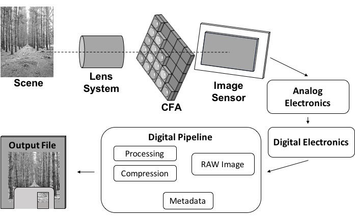
An abstract model of noise within image sensors can be developed by first focusing on what is known as the image pipeline (Figure 3). This pipeline is the process through which an optical image is converted and processed as an electronic signal to result in a digital image capable of being saved in the multiple formats commonplace today. Each element of the pipe adds an element of noise to the signal resulting in an additive noise model [12]. Through careful analysis of this pipeline, a noise model has been developed (Figure 4).
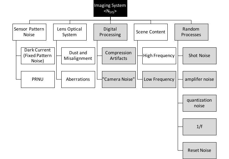
For a single image, the discrete sources of noise can be modelled as an additive combination of sensor pattern noise, lens optical effects, digital processing artefacts, scene content and random process [12]. To analyse the noise model for forensic advantage, the focus is linked to the areas that are related to the image sensor itself, namely the optical effects caused by integrated filters and lenses, noises caused by semiconductor physics of the sensor and integrated “on-chip” electronics, and the impact of the environment the sensor operates within. Such a focus allows the image sensor to uniquely describe the camera and not the parallel processes an image runs through before saving.
To determine which noise dominates a complete SNR analysis must be undertaken [12]. An SNR analysis is not the focus of this paper and is left as future work.
3.1 Optical Effects
To isolate the image sensor within the model, the first step is to ensure all other contributions of noise from the image pipeline have been eliminated. It is seen in Figure 3 that before entering the sensor, light first must pass through a lens system. Lens systems are not without error. Aberrations in multi-lens design and the lens itself include spherical aberration, coma, astigmatism, the curvature of field, distortion and chromatic aberration (a particular case of spherical aberration). These are commonly referred to as the primary or third-order Seidel Aberrations after the work of Ludwig von Seidel in 1857 [16]. Each aberration causes the light rays travelling to deviate in some manner from the optical axis of the lens resulting in optical noise which can be confined to either a pixel, group of pixels or the whole image. The relevant mathematical proof behind each aberration has been well explored in the literature, and many texts have been written on the topic [17].
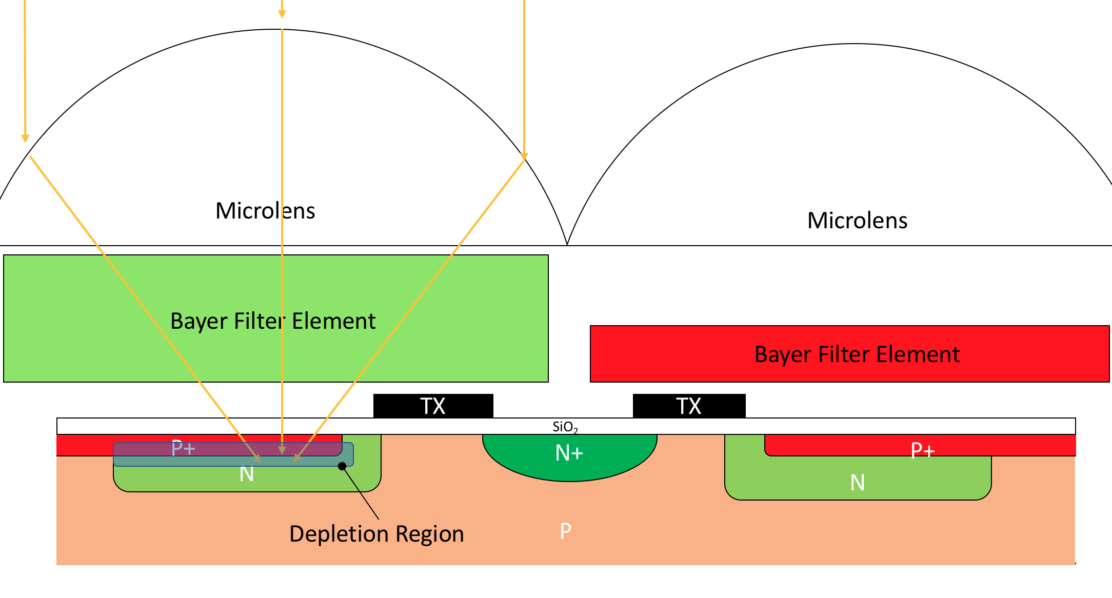
In addition to the lens system, each image sensor has integrated by design an optical colour filter array (CFA) to ensure colour images can be obtained from broad wavelength light-sensitive silicon. To focus light onto the photosensitive area of the pixel, each pixel also includes a microlens (Figure 5). Should any of these elements be incorrectly manufactured additional noise will be introduced to the system per the same aberrations as above.
Finally, due to physical properties of light, namely Planck-Einstein’s Formula, each discrete photon carries different levels of energy according to the wavelength it is travelling at:
| (3) |
where h is Planck’s constant , c is the speed of light, and is the wavelength. This energy results in longer wavelengths penetrating deeper into the sensor before being absorbed [12], affecting photon shot noise.
Optical effects have already been shown to be useful for forensic advantage using discrete lenses and CFA processing artefacts as the identifier. This identification has been achieved primarily through the use of radial lens distortions [18] and CFA interpolation algorithms [19]. What has not been shown is how variance in the CFA elements construction may affect penetration of photons to the sensor substrate below. Additionally, aberrations within the integrated microlens have yet to be included in the consideration of the overall noise profile since the sensor contains these elements that physically cannot be removed without destruction. This integrated microlens provides a point of difference that may be exploited for forensic advantage or otherwise contaminate the noise profile of the underlying silicon.
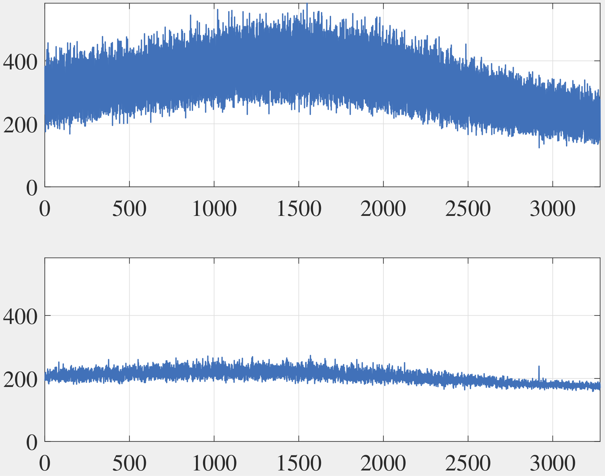
To illustrate the optical effects a side by side comparison of pixel intensities across a single row of an image taken with two separate lens systems is shown in Figure 6. In this graph, the top figure represents a row 1024 of a 2048x2048 image taken by an integrated lens. The bottom section displays the same row as taken with a pinhole lens. The pinhole image was taken with a suitable exposure time to ensure that the amount of light entering the sensor was the same. It is clear that the optical effects are removed since the variation of the pixel intensities is decreased in the pinhole image. This is most obvious towards the centre of the row where the intensity of the pixel is mostly uniform for the pinhole, however it increases for the lens. Such an aberration would be seen in an image as vignetting.
3.2 Semi-Conductor Physics
The basic operation of a photodiode has been described above in section 2. The primary process is to fill the N-well region of the photodiode with electrons in proportion to the number of photons that have excited the sensor. Under normal operation, however, the number of photon-induced electrons is combined with dark current electrons caused by the physical properties of the PN junction. Three primary sources generate this dark current: irregularities in the silicon structure, diffusion current due to Fick’s law and depletion region current which follows Ohm’s Law [20].
The various sources of dark current are complicated to model. This complexity is also in part due to issues with generation in multiple regions as dark current is not just generated in the photosensitive region. These regions include the depletion region, the field-free region and the surface of an oxide layer interface, as well as dark current increasing exponentially with temperature [12].
With much work devoted to the subject, it is often enough to model these interactions by the following [12]:
| (4) |
Where is the detector area, is the integration or exposure time, is the charge of an electron coul and is the dark current density which is proportional to:
| (5) |
where is Boltzmann’s constant, J/K, is the temperature in degrees Kelvin and () is the difference in bandgap energies for the impurity carrier and the primary carrier respectively.
From here it is possible to estimate the dark current at a specific temperature from a known image sensor at a given exposure time.
These dark current electrons will be combined with the photon generated electrons to fill the N-well region:
| (6) |
Since no silicon wafer is without defect and no two pixels are uniformly the same it is seen that the dark current will be measurably different between two pixels, however, is usually treated as uniform and quasi-stable for a sensor as a whole [21].
At the heart of the operation of an image sensor is the N-well region filling with electron generated photons thanks to the photoelectric effect at the depletion region between a PN junction at the N-well region. Since the size of this well differs from pixel to pixel, and sensor to sensor, it is possible to create a unique signal or fingerprint from the PRNU noise. This concept is the work of [1] which focuses on how N-well of each pixel can be filled to an equal amount via photonic energy. Each pixel is then read out via the well described processes and ultimately saved as an image. The slight variation of each pixel is measured on a pixel to pixel basis due to the differences in the ability of the PN junction of the photosensitive region to recombine photons.
It has been stated that dark current can be ignored for forensic purposes due to dark-frame removal [1], the subtraction of a frame exposed without opening the shutter of the same length of time immediately before taking an image. However, since the N-well region can be filled with electrons via dark current generation (equation 6), it is theoretically possible to measure a unique PNU signal in the same manner with the dark current being the excitation source rather than photons.
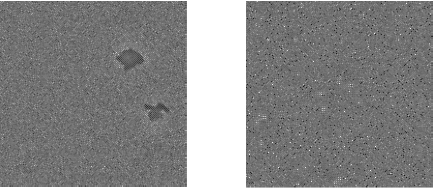
Since dark current density increases exponentially with temperature and proportionally with exposure time it is theoretically possible to completely saturate the N-well region with electrons generated purely from dark current, especially if the pixel pitch is small, as seen in mobile devices. By controlling these two parameters, it is proposed that a valid unique fingerprint can be obtained from a sensor using dark current electrons alone. Such a fingerprint is demonstrated in Figure 7. Demonstrating the reliability of such a fingerprint in a forensic context is beyond the scope of this paper and will be demonstrated in future work. However, to demonstrate that the fingerprints are indeed similar some observations are made. Within the dark current fingerprint the Kurosawa hot pixels [22] are required to be suppressed for an accurate comparison. This results in a salt and pepper noise artefact present within the fingerprint. Additionally, since light is not used to generate the fingerprint there is no contamination from dust as seen in the PRNU reference pattern.
| Temp (∘C) | 0∘ Rotation | 90∘ Rotation | 180∘ Rotation | 270∘ Rotation |
|---|---|---|---|---|
| 20 | 0.0219 | 1.30e-03 | 2.00e-03 | 1.70e-03 |
| 45 | 0.0408 | -8.68e-04 | 1.28e-05 | 3.50-05 |
| Temp (∘C) | 0∘ Rotation | 90∘ Rotation | 180∘ Rotation | 270∘ Rotation |
|---|---|---|---|---|
| 20 | 0.0335 | 1.10e-03 | 2.00e-03 | 7.23e-05 |
| 45 | 0.0740 | -7.56e-04 | 1.28e-04 | -2.64-08 |
| Temp (∘C) | 0∘ Rotation | 90∘ Rotation | 180∘ Rotation | 270∘ Rotation |
|---|---|---|---|---|
| 20 | 1.30e-03 | -8.01e-04 | 7.67e-04 | 1.30e-03 |
| 45 | 8.733-04 | -1.20e-03 | -7.77e-05 | -9.31-04 |
Demonstrating that the dark current fingerprint is correlating to the PRNU fingerprint a set of correlations is calculated for a single image dark current fingerprint at T=20∘C and 45∘C against a 100 image PRNU reference pattern (Table 1). The PRNU reference pattern is rotated 90∘, 180∘ and 270∘ as a proxy for a deliberate mismatch to ensure correlation is indeed occuring with the reference pattern and not an arbitary artefact of the sensor design. This is repeated for another camera in table 2 with the results confirming the previous demonstration. Finally, to ensure that the correlation is between the excitation of the silicon and not the read out of the sensor design itself half the PRNU reference pattern is swapped with the other half of the reference pattern to create a deliberate mismatch while maintaing colour filter rotation. These results are shown in table 3 with no significant correlation detected. These results demonstrate our hypothesis that a dark current fingerprint can be generated which may form as a substitute for the current PRNU methodologoy. A full analysis is left as future work.
4 Micrometer Imagery
To illustrate these concepts we have discussed above a cross-sectional image of a Sony IMX219PQ [23] image sensor was taken under a scanning electron microscope. Using an FEI Dual Beam Helios Nano Lab 600 [24] scanning electron microscope, two excavations were made into a Sony IMX219PQ CIS. Since the CIS is conductive, no sample preparation is required before scanning. First, a layer of platinum is deposited above the area to be excavated to prevent fracturing (Figure 8). After the platinum is deposited a process of staged cuts are made using a gallium ion beam to create an excavated area through the sensor that can be imaged (Figure 9).
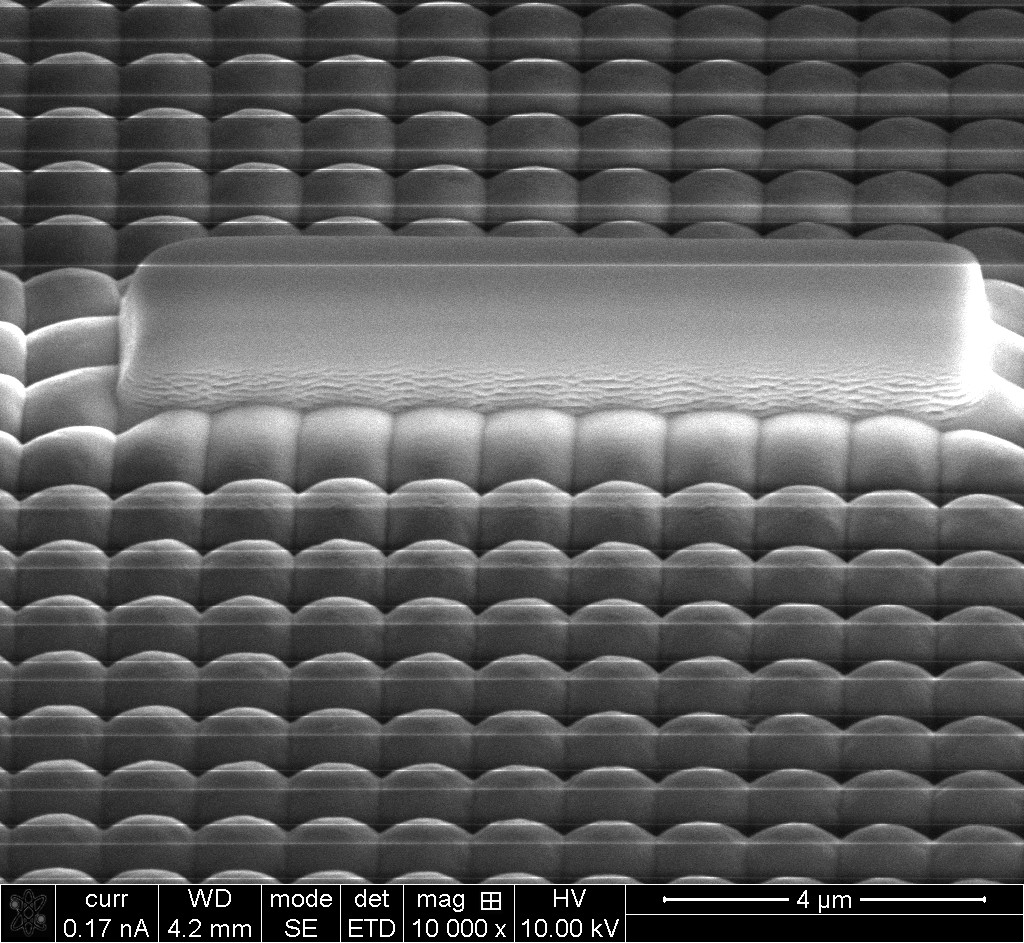
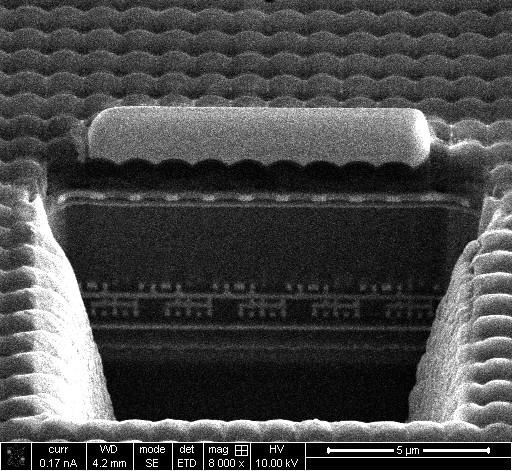
Using a magnification of 20,000x, a current of 0.17nA and voltage of 10kV, images are then obtained of the top layers of the integrated CIS containing the pinned photodiode. Since our study is not concerned with the readout circuitry, we exclude it from our observations. The process is repeated for a diagonal cross section to ensure multiple pixels across CFA regions are obtained.
In Figure 10 a layered PPD architecture is seen as expected. This PPD architecture uses a shared pixel concept with multiple transfer points (shown as TX). Using Energy-dispersive x-ray spectroscopy, the architecture can be determined in detail. Elements detected in the EDX analysis include Platinum, Carbon, Gallium, Oxygen, Silicon, Tungsten, and Titanium. The presence of gallium and platinum must be excluded since they are used in the SEM processes outlined above. However, using reasonable assumptions, the areas of the CIS in the image as shown can be reverse engineered. An isolation oxide layer directly below the PN junction made from titanium dioxide is observed as part of the structure. This TiO2 layer electrically isolates the PN junction from the underlying substrate and also isolates any photons from further penetrating into the underlying substrate [12].
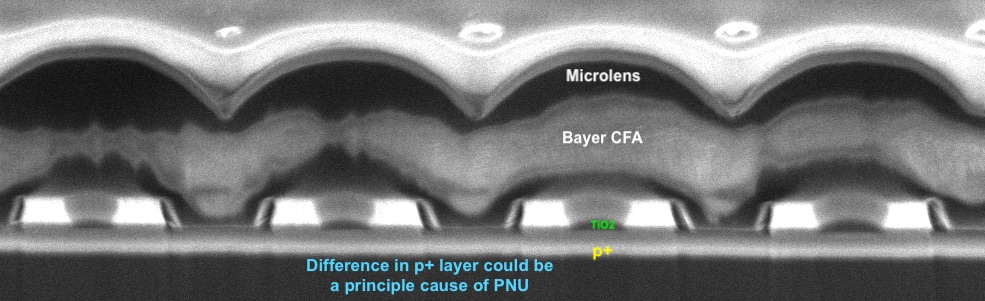
To explain the structure and operation we refer to [23]. Light first enters the sensor via the microlens array and is then filtered using a Bayer filter. The IMX219PQ sensor has a traditional ”R, G, and B primary colour pigment mosaic filters” CFA [23]. These filter elements are not uniform in their construction, and it is seen that even cells of the same colour have different widths (Figure 10). From Equation 3 it is clear that this will result in different wavelengths being filtered out on a pixel by pixel basis rather than just the three principal components being isolated by the chemical composition of these layers. This filtering will cause chromatic distortion. While the cause of variation in the CFA layer is impossible to determine from this image, an indication is given from the P+ pinning layer directly below. Since the CMOS process manufactures each layer on top of the previous layer, variations in the layers below will cause issues in the layers above. It is seen that the width of the pinning layer is different from pixel to pixel in the cross-sectional view not just in width but also in length. This pinning layer will affect the performance of the photosensitive PN region and even the dark current of each pixel.
Since there are variations between each pixel, it may be possible to to isolate and hence exploit these variations, to create better processes to isolate a unique fingerprint for the sensor.
5 Conclusion
SPN has shown to be a promising area of research for answering provenance questions relating to imagery. It still suffers from reliance on large data sets ideally constructed from flat fielded images and a-priori information that is not always apparent or readily available to forensic investigators in the field. By rethinking the noise model of a digital camera, SPN can be isolated as an element that is primarily dependent on the physical silicon that each image sensor is built from, regardless of technology. From this analysis, it can be seen that there are alternative ways to create the unique fingerprint that will not rely on large data sets or mass computational resources. An example, the subject of current work, is the exploitation of dark current.
6 Acknowledgements
This research did not receive any specific grant from funding agencies in the public, commercial, or not-for-profit sectors. The authors acknowledge the facilities, and the scientific and technical assistance, of the Australian Microscopy and Microanalysis Research Facility at Adelaide Microscopy, the University of Adelaide. This research is supported by an Australian Government Research Training Program (RTP) Scholarship and forms part of a thesis chapter.
References
- [1] J. Lukáŝ, J. Fridrich, M. Goljan, Digital camera identification from sensor pattern noise, IEEE Trans. Inf. Forensics Security 1 (2) (2006) 205–214.
- [2] M. Goljan, J. Fridrich, T. Filler, Large scale test of sensor fingerprint camera identification, in: Media Forensics and Security, Vol. 7254, International Society for Optics and Photonics, 2009, p. 72540I.
- [3] H. Farid, Photo Forensics, MIT Press, 2016.
-
[4]
A. A. C. SWINTON, Electric
television, Nature 118 (2973) (1926) 590–590.
doi:10.1038/118590a0.
URL http://dx.doi.org/10.1038/118590a0 - [5] H. Iams, A. Rose, Television pickup tubes with cathode-ray beam scanning, Proceedings of the Institute of Radio Engineers 25 (8) (1937) 1048–1070. doi:10.1109/JRPROC.1937.228423.
-
[6]
A. A. C. SWINTON, Distant electric
vision, Nature 78 (2016) (1908) 151–151.
doi:10.1038/078151a0.
URL http://dx.doi.org/10.1038/078151a0 - [7] W. Boyle, G. Smith, Buried channel charge coupled devices, uS Patent 3,792,322 (Feb. 12 1974).
- [8] W. Boyle, G. Smith, Three dimensional charge coupled devices, uS Patent 3,796,927 (Mar. 12 1974).
- [9] K. Matsumoto, T. Nakamura, A. Yusa, S. Nagai, A new mos phototransistor operating in a non-destructive readout mode, Jpn. J. Appl. Phys. 24 (5) (1985) L323–L325.
- [10] E. R. Fossum, Active pixel sensors: Are ccds dinosaurs?, Vol. 1900, 1993, pp. 2–14.
-
[11]
A. J. Theuwissen,
Cmos
image sensors: State-of-the-art, Solid-State Electronics 52 (9) (2008)
1401–1406.
doi:10.1016/j.sse.2008.04.012.
URL http://linkinghub.elsevier.com/retrieve/pii/S0038110108001317 - [12] G. C. Holst, ”CMOS/CCD sensors and camera systems”, JCD Publishing, 2011.
-
[13]
A 3M pixel multi-aperture
image sensor with 0.7 m pixels in 0.11 m cmos, 2008, pp. 48–594.
doi:10.1109/ISSCC.2008.4523050.
URL http://ieeexplore.ieee.org/document/4523050/ -
[14]
ePHOTOzine,
Complete
guide to image sensor pixel size.
URL https://www.ephotozine.com/article/complete-guide-to-image-sensor-pixel-size-29652 - [15] S. Knight, S. Moschou, M. Sorell, Analysis of sensor photo response non-uniformity in raw images, in: International Conference on Forensics in Telecommunications, Information, and Multimedia, Springer, 2009, pp. 130–141.
- [16] P. L. V. Seidel, Über den Einfluss der Theorie der Fehler, mit welchen die durch Optische Instrumente gesehenen Bilder behaftet sind, und über die mathematischen Bedingungen ihrer Authebung., ”Abhandlungen der naturwissenschaftlich-technischen Commission der Bayerischen Akademie der Wissenschafte.
- [17] F. A. Jenkins, H. E. White, Fundamentals of optics, Tata McGraw-Hill Education, 1937.
-
[18]
K. S. Choi, E. Y. Lam, K. K. Y. Wong,
Source
camera identification using footprints from lens aberration, Vol. 6069 of
SPIE Proceedings, SPIE, 2006, p. 60690J.
doi:10.1117/12.649775.
URL http://proceedings.spiedigitallibrary.org/proceeding.aspx?doi=10.1117/12.649775 - [19] S. Bayram, H. Sencar, N. Memon, I. Avcibas, Source camera identification based on cfa interpolation, in: Image Processing, 2005. ICIP 2005. IEEE International Conference on, Vol. 3, IEEE, 2005, pp. III–69.
-
[20]
E. W. Bogaart, W. Hoekstra, I. M. Peters, A. C. M. Kleimann, J. T. Bosiers,
Very low dark current ccd
image sensor, IEEE Transactions on Electron Devices 56 (11) (2009)
2462–2467.
doi:10.1109/TED.2009.2030642.
URL http://ieeexplore.ieee.org/document/5247096/ - [21] R. M. Smith, G. Rahmer, Pixel area variation in ccds and implications for precision photometry, in: High Energy, Optical, and Infrared Detectors for Astronomy III, Vol. 7021, International Society for Optics and Photonics, 2008, p. 70212A.
- [22] K. Kurosawa, K. Kuroki, N. Saitoh, Ccd fingerprint method-identification of a video camera from videotaped images, in: Image Processing, 1999. ICIP 99. Proceedings. 1999 International Conference on, Vol. 3, IEEE, 1999, pp. 537–540.
-
[23]
Sony,
IMX219PQ
product brief.
URL https://www.sony-semicon.co.jp/products_en/IS/sensor1/img/products/ProductBrief_IMX219PQ_20160425.pdf -
[24]
FEI,
Helios
nanolab 450 / 450 s / 450 ml / 650 / 600i user operation manual.
URL https://mc2.engin.umich.edu/wp-content/uploads/sites/227/2015/11/Helios.pdf