Impact ionization dynamics in small band-gap 2D materials from a coherent phonon mechanism
Abstract
We study theoretically the role of carrier multiplication due to impact ionization after an ultrafast optical excitation in a model system of a quasi-two dimensional material with a small band gap. As a mechanism for the photo-induced band gap narrowing we use coherent phonons, which mimics the quenching of an insulator phase. We discuss the importance of impact ionization in the ultrafast response, and investigate the interplay between carrier and band dynamics. Our model allows us to compare with recent experiments and identify signatures of carrier multiplication in typical electronic distribution curves as measured by time-resolved photoemission spectroscopy. In particular we investigate the influence of the shape of the bands on the carrier multiplication and the respective contributions of band and carrier dynamics to electronic distribution curves.
I Introduction
Recent developments in time- and angle-resolved photoemission spectroscopy (trARPES) have opened up the possibility to study the material response after ultrafast optical excitation using photoemission techniques. Rohwer et al. (2011); Sobota et al. (2014); Eich et al. (2014) This progress has facilitated the study of correlated and nanoscale quantum materials. Smallwood et al. (2016) Besides graphene, Gierz (2017); Gierz et al. (2013); Stroucken et al. (2013); Mihnev et al. (2016); Kadi et al. (2015) other two-dimensional materials, Bhimanapati et al. (2015) in particular transition-metal dichalcogenides (TMDC), Chhowalla et al. (2013); Voiry et al. (2015); Steinhoff et al. (2016) have been the center of current investigations. Associated with this topic is an active interest in metal-insulator transitions. Hellmann et al. (2012) Besides Mott insulators Ghatak et al. (2011); Cheiwchanchamnangij and Lambrecht (2012); Chernikov et al. (2015); Chen et al. (2016); Steinhoff et al. (2016, 2017); Moon et al. (2018) these transitions can appear as excitonic and Peierls insulators, where a formation of a charge density wave (CDW) and a periodic lattice distortion occur. Grüner (1988) However, charge density waves are observed in many solids and their origin is still under debate. Zhu et al. (2015); Flicker and Van Wezel (2015); Cho et al. (2016); Leroux et al. (2018); Nakata et al. (2018) Further, changing the symmetry of a material via optically induced phase transitions offers new ways to manipulate material properties on ultrafast timescales. Wall et al. (2012); Mizokawa et al. (2009) Research about the ultrafast response of two dimensional materials like TMDC in connection with their rich electronic phase diagrams, e.g., superconductivity Sykora et al. (2009); Kim et al. (2015) or CDW phases, may well be important for understanding the basic physics for the design of future ultrafast (optoelectronic or optospintronic) devices. Ritschel et al. (2015); Gu and Rondinelli (2016); Khitun et al. (2016)
Materials like 1T-TaS2, 2H-TaSe2, and 1T-TiSe2 have been studied in some detail, Rossnagel (2011); Porer et al. (2014); Zhang et al. (2018) but there still is a controversy about the origin of the CDW phases in those materials, especially for 1T-TiSe2. In Refs. Monney et al., 2009, 2010; Cazzaniga et al., 2012; Monney et al., 2012a; Li et al., 2007; Monney et al., 2011; Kogar et al., 2017; Chen et al., 2017; Pasquier and Yazyev, 2018; Golež et al., 2016 an excitonic insulator mechanism was identified. However, there are also arguments that an electron-lattice interaction with the help of the Jahn-Teller effect leads to a Peierls-like CDW transition and the accompanying opening of a gap. Rossnagel et al. (2002); Karam et al. (2018); Hughes (1977); Hellgren et al. (2017) To our knowledge, the prevailing explanation is a combination of exciton-formation and electron-phonon coupling. Kidd et al. (2002); van Wezel et al. (2010); Monney et al. (2012b); Van Wezel et al. (2010); Phan et al. (2013); Watanabe et al. (2015); Bianco et al. (2015); Monney et al. (2016); Kogar et al. (2017); Chen et al. (2017); Pasquier and Yazyev (2018); Karam et al. (2018); Maschek et al. (2016); Singh et al. (2017); Hellgren et al. (2017) In this context, the chirality of the CDW Ishioka et al. (2010); Castellan et al. (2013); Silva et al. (2018); Hildebrand et al. (2018) and a softening of phonon modes Weber et al. (2011); Maschek et al. (2016) have also been discussed.
The present paper is devoted to a study of non-equilibrium carrier dynamics during an optically induced phase change between an “insulator” and a “metallic” phase in a system with a small band gap, where carrier-scattering processes may lead to carrier multiplication due to impact ionization. On the basis of experimental results and a simple model calculation it has recently been argued in Ref. Mathias et al., 2016 that in 1T-TiSe2 excitation by an ultrafast optical pulse induces carrier multiplication and gap-closing dynamics, which amplify each other during the quenching of the CDW phase. In this paper, we investigate theoretically in more detail this interplay between carrier dynamics (in particular, carrier multiplication) and quasi-particle band-structure change, i.e., gap quenching. We employ a dynamical model that is capable of describing aspects of the ultrafast response of small band-gap 2D materials. We assume an electron-phonon based mechanism behind the formation of the CDW state, but we do not attempt a microscopic description of the complete change between insulator and metallic phase. Instead, we restrict our attention to the onset of the phase transition starting from the CDW insulator phase, and model the relevant lattice dynamics by coherent phonons. These coherent phonons interact with the optically excited electronic dynamics and, in turn, change the quasi-particle band structure via a modulation of hybridization between electronic orbitals centered at the ions that oscillate with the coherent phonon. An important goal of this paper is to study the interplay between carrier multiplication effects and quasi-particle band-structure dynamics by dynamical calculations for a concrete mechanism. In particular we explore the consequences for quantities accessible in recent experiments, where carrier multiplication and band-strucure dynamics cannot easily be disentangled. Mathias et al. (2016) In particular, we study the influence of different excitation scenarios, and compare the results for different band structures (parabolic and Mexican-hat shaped bands).
The outline of this paper is as follows. In Sec. II we first introduce a model composed of a tight-binding band structure and carrier-phonon interaction in which the quenching of the insulator phase is due to the coupling to coherent phonons. In a nonequilibrium situation, this electron-phonon coupling results in the change in quasi-particle bands associated with a Peierls-like transition. In Sec. III we set up the equations of motion for the relevant distribution functions including the optical-excitation contribution and Coulomb interaction. Numerical results are presented in Sec. IV. We discuss here in particular the influence of model parameters on the carrier dynamics the interplay of carrier multiplication and gap-closing dynamics and their signatures in electronic distribution curves. Technical details concerning the tight-binding model and the numerical solution of the dynamical equations including the gap dynamics are collected in Appendices A and B. We conclude the paper in Sec. V.
II Quasi-particle Electronic Structure Calculation
As we want to describe carrier dynamics that accompany the quenching of a small band-gap insulator phase, we first need to address how the quasiparticle band structure changes during this phase transition. While a variety of different models for charge-density-wave insulators exist, Zhu et al. (2015) the classification for materials like 1T-TiSe2 or 1T-TaS2 is not straightforward. Among other reasons, this is because electron-electron and electron-phonon interactions may both play an important role in the phase transition dynamics. As we focus here on the carrier dynamics, it is beyond the scope of this paper to include such complex interdependencies. Instead of determining the insulator phase from the normal phase, we start from a TB model of the band structure in the insulator phase and describe the quenching of this phase as an effective misalignment of the atomic positions of the different atoms in the unit cell. This effective atomic displacement after an optical excitation enters our calculation as a coherent phonon.
II.1 Tight-Binding Model
We employ a tight-binding model to describe a quasi-two dimensional material with two atomic species Ad and Ap in the insulator phase. The parameters are chosen such as to reproduce some important characteristics of electronic states in TMDCs. In the case of a TMDC, the atomic species Ad is the transition metal (e.g. Ti) with d-type or f-type valence orbitals and the atomic species Ap is the chalcogen (e.g., Se) with p-type valence orbitals. For instance, in Refs. van Wezel et al., 2010; Van Wezel et al., 2010 it was found that for 1T-TiSe2 only the three hopping parameters ddσ, ppσ and pdπ contribute significantly to the behavior of states with energies close to the Fermi energy. This allows one to use a restricted model that includes only these hopping parameters.
As we do not attempt a microscopic model of the physics underlying the phase transition and as we are mainly interested in the electronic dynamics close to the small band gap, which is the indicator of the CDW and typically opens at high symmetry points, such as or points, we use a simple two-band tight-binding model to capture the characteristics of the carrier and band dynamics around the gap after an ultrashort optical excitation. We explain the relation of this ansatz to existing tight-binding models of transition-metal dichalcogenides in Appendix A. For now, we take the model tight-binding hamiltonian in the form
| (1) |
where , are the on-site energies, and , , , are the tight-binding coupling-elements and is the distance vector between two neighboring unit cells. As we do not include spin-orbit coupling, we do not explicitly write out the spin-dependence s in the following.
This model yields a conduction band mainly consisting of a d-type transition metal orbital and a valence band mainly originating from a p-type chalcogen orbital. In the neighborhood of this point the band structure has the shape of a Mexican hat with a small band gap and pronounced band mixing for the model parameters chosen here, see Sec. IV. Close to the high symmetry point the band structure possesses rotational symmetry. We stress that the simplicity of this model and the high symmetry are not too restrictive, because a fast angular redistribution of carriers due to electron-phonon scattering Mittendorff et al. (2014) will smooth out the effects of anisotropy, and our results should also be transferable to non-parabolic band structures.
II.2 Quasi-particle band dynamics and the effective Hamiltonian
This subsection is concerned with determination of the carrier states that accompany the onset of the phase change and that we will sometimes refer to simply as “band dynamics”. We do not attempt a microscopic ab-initio description of the coupled electron-ion system and the transition from normal phase transition to charge-density wave phase. Instead, we use an effective hamiltonian for the system in the charge-density wave state that already incorporates the lattice distortion induced by the electron-phonon interaction. In this model, the coherent phonon leads to an ionic displacement that causes a change of the hybridization between electronic orbitals centered at different ions, which changes the effective hamiltonian. Due to the dependence on the phonon dynamics, the effective hamiltonian becomes time dependent.
We begin with the free phonon Hamiltonian for the coherent phonon, i.e. ,
| (2) |
describes a coherent phonon (cpn) with that leads to a distortion consistent with the symmetry of the material, e.g., the A1g mode, in which the two kinds of atoms are displaced in the unit cell. The coherent phonon couples to the electrons by modulating the p-d hybridization
| (3) |
where is the matrix element for the coupling of electrons to the coherent phonon in the orbital basis. We assume for simplicity that this matrix element is -independent.
The interaction of electrons with a coherent phonon includes a mean-field contribution
| (4) |
where is the coherent phonon amplitude, and denotes the orbital index. The mean-field part of the coupling hamiltonian to the coherent phonon does not contain phonon operators and can be combined with to an effective hamiltonian for the carrier system that describes the states around the Fermi energy
| (5) |
As is time dependent its eigenvalues and eigenvectors are calculated for every time-step of the dynamical calculation. Thus, matrix elements and generally involve time-dependent basis states as will be discussed in Appendix B. In this time-dependent eigenbasis, can be interpreted as the occupation of the state at that time and the corresponding phonon matrix element. In particular, the matrix element in the orbital basis is related to matrix elements and in the time-dependent basis. Assuming that the coherences in this equation-of-motion die out faster than the dynamics of interest, we obtain the equation of motion
| (6) |
The coupling matrix elements , which are off diagonal with respect to the orbital index, influence the band occupations via matrix elements, which are diagonal with respect to the band index, and thus drive the coherent phonon amplitude Eq. (6).
III Carrier dynamics via equation of motion technique
III.1 Optical excitation
We model the optical excitation after a recent experiment on 1T-TiSe2 in Ref. Mathias et al., 2016, where carriers were excited with an 1.6 eV pulse around 200 meV above the Fermi level into a Ti 3d band around the M-point. Around this high symmetry point, only a small band-gap exists between the Ti 3d band and a back-folded Se 4p band. As the holes, which are likely created in a Se 4p(x,y) bands, never appear close to the Fermi surface, we do not include these band states in our two-band tight-binding model. Further, the dispersions of the bands of interest are different (i.e., have very different curvature in our simplified case), so that in the first few hundred femtoseconds the excited holes have no chance to reach the Fermi surface and no efficient contribution to the ultrafast carrier and band response around Fermi surface is possible, as found in experiment. Mathias et al. (2016) Thus, we model the optical excitation between the conduction band “c” mainly originating from the d-type orbital of atom species Ad and a third band below the Fermi surface by
| (7) |
and
| (8) |
where , and we have again suppressed the spin index.
The major contribution to the coherent phonon amplitude dynamics originates from the excitation of electrons into the conduction band. This is in accordance to situations, where optical excitation can trigger a displacive A1g CDW amplitude mode by exciting electrons from bonding to antibonding states, e.g., in 1T-TiSe2. Monney et al. (2016) It is also supported by other investigations, which have found that the A1g mode shows a strong coupling to conduction electrons. Donkov et al. (2009); Chakraborty et al. (2012) While the effects of excitonic contributions likely have to be included to obtain quantitative agreement (e.g., for the speed of the gap dynamics), Mathias et al. (2016) the qualitative picture of the onset of a phase transition due to ultrafast optical excitation can be described by coherent phonons. In such a model, carrier multiplication also has an contribution to the dynamics of the coherent phonon amplitude, as we show in the following.
III.2 Carrier-carrier Coulomb scattering
The Coulomb scattering to describe the carrier dynamics in the first few hundred femtoseconds after the ultrafast optical excitation is also included in the equation of motion for the density matrix. As the Coulomb interaction leads to transitions between quasiparticle states, which change dynamically, we use time-dependent Bloch states. This entails not only the correction of the band-energies but also a re-calculation of the interaction-matrix elements. In general, it is associated with a transformation of diagonal density-contributions into off-diagonal coherence-contributions in conjunction with correlated correction-terms in the equation-of-motion. This general consequences are described and the level of approximation for the system under investigation is explained in appendix B, where we assume a sufficiently high dephasing for these coherences, which is likely for the system under investigation, and hence the off-diagonal coherence-contributions in conjunction with correlated correction-terms in the equation-of-motion can be neglected. Thus, we implement the time-dependent basis in the description of the carrier dynamics using time-dependent band-energies and wave-functions including time-dependent Coulomb-matrix elements due to the basis transformation with of-course a time-dependent screening. Importantly, the band dynamics here leads to an additional re-distribution of carriers into the new equilibrium distribution and changes the ratio between intra and interband scattering pathways.
The derivation of the Coulomb scattering equations itself can be established in various ways. For instance, with cluster expansion techniques or with the Green’s function technique under the use of the Kadanoff-Baym equations, by applying the second-order Born approximation for the self-energy.Steinhoff et al. (2016) For the carrier-carrier scattering we neglect coherences and obtain the following equation of motion for the Coulomb scattering in Markov approximation
| (9) |
with
| (10) | ||||
| (11) | ||||
| (12) | ||||
| (13) |
where are the screened Coulomb-Matrix elements, is the carrier distribution and the corresponding energy on for the band . The spin-index is neglected. The screened Coulomb potential is
| (14) |
with the overlap integrals
| (15) |
and . Further, are the eigenfunctions of the time-dependent tight-binding Hamiltonian in Eq. (5), is the unscreened Coulomb potential including a background dielectric constant and the normalization area.
In the derivation of the Coulomb scattering equations, the screened Coulomb potential can be naturally included. The time-dependent screening of the Coulomb interaction is taken into account using the static limit of Lindhard dielectric function
| (16) |
where are the Coulomb-matrix elements calculated from the unscreened Coulomb potential .
IV Numerical results
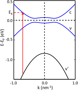
To investigate the ultrafast response of a small band-gap 2D material after an ultrafast optical excitation, and particularly of the role of impact ionization and carrier multiplication in the conduction band, we assume the setup shown in Fig. 1, which we discuss here first. From the tight-binding Hamiltonian Eq. (1) from Sec. II.1, we obtain two Mexican-hat shaped bands close to the Fermi surface, a conduction band “c” and a valence band “v”. Further, we assume a lattice temperature of 100 K and the band gap is measured as the nearest distance between the two Mexican-hat shaped bands, which is 100 meV for the unexcited band structure. The lattice temperature is below the transition temperature and the band-gap is adapted to that of the CDW phase of a typical material like TiSe2 as reported for example in Ref. Monney et al., 2010. The optical excitation is modeled as excitation originating from a third band “” not included in the two-band tight-binding model as explained in Sect. III.1. As indicated in Fig. 1, the band is far below the Fermi surface and the ultrafast optical excitation by a pulse with a 1.6 eV photon energy excites carriers into the conduction band around 200 meV above the Fermi surface as measured by trARPES experiments on TiSe2 reported in Ref. Mathias et al., 2016. For the unexcited material we assume a Fermi distribution and thus we obtain a nearly empty conduction band with negligible band corrections due to coherent phonons, see Sect. II.2 and weak screening. After the ultrashort optical excitation, effects such as band dynamics induced by coherent phonons and a carrier redistribution due to Coulomb scattering, see Sect. III.2, will determine the material response as investigated in the following.
IV.1 Characteristics of band- and carrier response
First, we discuss the essential characteristics of the dynamical results for the excitation described above. A technical aspect is to clarify and investigate the effect of the basis transformation of the electron-phonon matrix element between the time-dependent basis of band states and the atomic eigenbasis, which creates -dependent phonon matrix elements from initially constant values in the atomic eigenbasis.
The Mexican-hat shaped electronic band-structure shown in Fig. 1 is modeled using the tight-binding parameters eV, eV for the on-site energies, and eV, eV for the coupling elements. For the coherent phonons, we take meV and ps-1. The electron-phonon matrix element controls the influence of the optical phonon on the band dynamics and plays an import role in our model. To study its influence, we present calculations using the values of meV and meV in the orbital basis for this matrix element. The optical excitation is patterned after the experimental conditions in Ref. Mathias et al., 2016 and taken to be a Gaussian pulse with 1.6 eV photon energy, temporal width of fs assuming a Rabi energy meV. This results in an excitation of electrons in the conduction band around 200 meV above the unexcited Fermi surface.
After analyzing the consequences of the -dependent basis transformation we will introduce a further simplified model which assumes an averaged value of the electron-phonon matrix element and neglect the influence of the basis transformation. In this case we treat the phonon matrix element as a parameter with meV.
IV.1.1 Band and carrier response after optical excitation
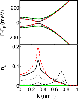
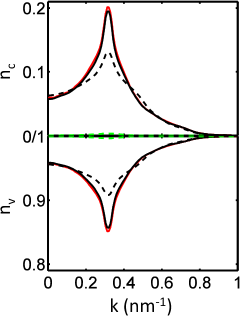
The essential characteristics of the dynamical results are discussed for the setup with meV, because effects of band renormalization and carrier multiplication are clearly visible in this case. In Fig. 2 snapshots of the band and carrier dynamics of the conduction band are shown. Before the optical excitation the valence band is full and the conduction band nearly empty. The band gap of the Mexican-hat shaped bands is 100 meV at the crease of the Mexican hat . At around 0 fs the ultrafast optical pulse excites carriers from the lower lying band into the conduction band c at around 200 meV above the unexcited Fermi energy cf. Fig. 1. Between -25 fs and 25 fs mainly optical excitation occurs, but also carrier scattering and the onset of impact ionization. The combination of these effects and the mexican-hat band structure lead to a small second peak at the band bottom . Due to the comparatively large band gap of 100 meV, the impact ionization initially is not very efficient. However, after 25 fs, i.e., after the optical excitation is over, the hot carriers in the conduction band lead to a gap closing due to the coherent phonon dynamics and a more efficient screening. The gap closing leads to a more efficient impact ionization, as will be discussed in detail in connection with Fig. 4. Fig. 4 supports the following scenario: The hot carriers relax from the first peak induced by the optical excitation via impact ionization into the second peak at the band bottom. The impact ionization induces a carrier multiplication in the conduction band, which results in a further gap closing. The smaller gap makes impact ionization even more efficient, which speeds-up the relaxation of the hot carriers, which is visible in the distances between the snapshots in Fig. 2, but more clearly in Fig. 4 below. Thus there is a mutual amplification between gap closing and impact ionization. The latter occurs predominantly at the band bottom of the mexican hat and thus feeds the second peak on the band bottom of the conduction band in Figure 2 until no more phase space for electron-electron scattering is available and a quasi-equilibrium distribution is reached.
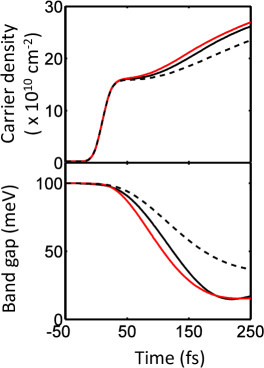
We next investigate details of the carrier and band-gap dynamics for the same parameters as in Fig. 2, which are marked by solid black lines in Figs. 3 and 4. We defer a discussion of the different parameters (dashed and red curves in Figs. 3 and 4) to the next subsection. The solid black lines in Fig. 3 shows the carrier distribution of the conduction and valence band 250 fs after the optical excitation. As the optical excitation is into the conduction band, the increase of the hole density around the top of the valence band in the first 250 fs after the optical excitation indicates the effect of impact ionization as all the carrier dynamics is exclusively due to Coulomb scattering. In Figure 4 the solid black lines depict the time-dependence of the conduction-band carrier density and the band gap. The fast increase of the carrier density due to the ultrafast optical excitation occurs around the center of the pulse at 0 fs. This induces a gap closing via coherent phonons that is clearly visible for times later than 50 fs. Finally, and importantly, there is a delayed increase of the carrier density that is exclusively due to impact ionization from carriers originating from the valence band. This impact ionization therefore effectively acts a carrier excitation mechanism which drives the distributions in the conduction and valence bands further away from equilibrium. The coupling of the nonequilibrium carriers to the coherent phonon increases the band-gap shrinkage further.
IV.1.2 Influence of electron-phonon matrix elements on response
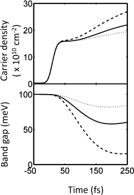
In Figure 3 and Figure 4 we study the influence of the electron-phonon coupling and also the consequence of using and an averaged value of the phonon matrix element . We first replace the electron-phonon matrix elements meV used so far by an averaged matrix element meV. With this replacement, we obtain similar final carrier distributions after 250 fs as shown in Figure 3, similar carrier densities and band-gap dynamics as shown in Fig. 4 and thus also a similar carrier multiplication of slightly above 70% at 250 fs. To show the sensitivity of the results on the electron-phonon coupling matrix element, we also show a calculation with meV. This leads to a sizable difference in the final carrier distributions, reduces the band-gap shrinkage and also the carrier multiplication to about 50 % for the setup with meV. Therefore, for a simulation of real materials and their electron-phonon matrix elements it is important to take into account the basis transformation. However, in the spirit of our model, we will use averaged electron-phonon matrix elements, which are capable of reproducing the dynamical calculations, albeit for a slightly different value of the electron-phonon matrix elements. This is sufficient for the more qualitative analysis of the present paper.
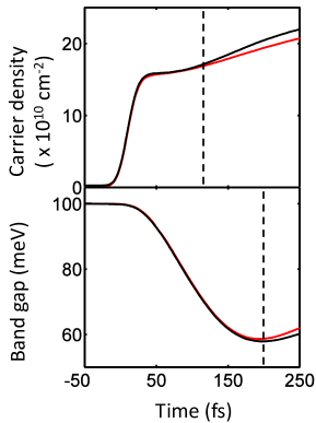
In Fig. 5 we analyze the influence of different values of the averaged electron-phonon coupling matrix element by comparing meV, 4.0 meV, and 6.0 meV. Because the quenching of the insulator phase is due to the coherent phonon dynamics, the gap closing depends on the strength of the electron-phonon matrix. Due to efficiency of the coupling between carrier and band dynamics, the mutual amplification between impact ionization and gap closing leads to a gap minimum of 15 meV for the setup with meV, 58 meV for the setup with meV and 81 meV for the setup with meV. Besides the gap closing also the carrier multiplication is visible in Fig. 5 via the time-evolution of the carrier density in the conduction band. After 300 fs a carrier multiplication of 74 % ( meV), 42 % ( meV), and 26 % ( meV) is reached.
IV.2 Comparison to experimental results and influence of different excitation scenarios
An important objective of this paper is to provide results that can be compared with recent experimental photoemission data. In particular, the energy distribution curves of photoemitted electrons cannot unambiguously be interpreted without some theoretical model. Mathias et al. (2016) As we cannot compute the cross sections that would be needed for a quantitative comparison with the energy distribution curves, we present a qualitative comparison using a broadening of the conduction and valence distribution by the typical experimental energy resolution of 150 meV (FWHM). The broadened distributions are defined by
| (17) |
where is a Gaussian of width . The important point for the comparison with experiment are the energy dependent features, not the numerical value of the s.
In the following, we first illustrate the spectral and kinetic response with the help of the broadened distributions using our two band model and the electron-phonon matrix element meV in the orbital basis including the basis transformation of the electron-phonon matrix elements. We first show results for our model using the band-gap of TiSe2 in the charge-density wave phase which are intended to be compared to electron distribution curves for small band-gap materials. Afterwards we analyze the dependence of the response on the optical excitation by a parameter study for different Rabi frequencies and excitation energies.
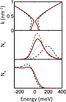
The broadened distributions for conduction and valence bands, together with the band dispersions are shown in Figure 6 for different times. We focus on the distribution of conduction electrons first. In the first 25 fs, the ultrafast optical excitation creates a peak in this distribution function at 200 meV above the Fermi energy. After 100 fs the hot-carrier relaxation due to impact ionization induced by the gap closing is clearly visible in the broadened distribution function. However, in a Mexican-hat shaped band-structure the interpretation of the broadened electron distribution is not straightforward because a time-dependent increase in the conduction band is a combination of band-dispersion effects and the on-going carrier multiplication. As we have seen in Figure 3 and Figure 4 the effects of carrier multiplication dominate the increase of the carrier signal at later times. The mutual amplification between impact ionization and gap closing, which has already been discussed, continues as shown by the snapshots for the band and distribution functions in Figure 6 until there is no more phase space for electron-electron scattering available and a quasi-equilibrium distribution is reached after 250 fs. Starting from a value of the band-gap that is realistic for small-bandgap material like 1-TiSe2 we thus obtain in our model calculation a signal of ultrafast carrier dynamics that is in agreement with experimental results, such as those reported in Ref. Mathias et al., 2016. Our calculated “signal” can be explained in terms of a mutual amplification between gap closing, which goes along with the quenching of the insulator phase, and impact ionization. In the present paper, the band gap dynamics are due to coherent phonons and are therefore applicable to a Peierls-like insulator. It is to be expected that a similar connection between gap closing and impact ionization occurs also for an excitonic-insulator phase-change mechanism. It may be even more pronounced in the excitonic-insulator case, because there the characteristic response times are faster than the response time of a Peierls insulator, cf. Ref. Hellmann et al., 2012, which indicates that the important electron-electron coupling matrix elements in that case are larger. However, because of the slower gap response in the Peierls (electron-phonon coupling) case, the connection between gap closing and carrier multiplication can be more easily disentangled in the model used here.
Turning to the broadened valence band distributions, shown in Fig. 6 (bottom), the holes at the top of the Mexican-hat shaped valence band created by impact ionization are hardly visible. This is because the broadening of the distribution function almost completely removes the dip in the microscopic valence band distributions shown in Fig. 3. This is in agreement with our earlier study using a parabolic valence-band and experimental results in Ref. Mathias et al., 2016. The dynamics of the Mexican hat introduces new features, such as the bump of the broadened valence band distribution around the top of the filled valence band, which is due to the changing band dispersion. The shift of the broadened distribution function is due to the band shift of the valence band as shown in Fig. 6 (top). These results give a simple microscopic picture of electronic dynamics underlying the electron distribution curves observed, e.g, in Ref. Mathias et al., 2016 for TiSe2. We plot and discuss the band and carrier dynamics in this paper up to about 250 fs, which is the onset of the phase transition. At longer times the system can go further into a different phase where the back-folded valence band disappears, or the system can return to the insulator phase by cooling processes due to carrier-phonon scattering. Both effects are not included in the present study and are left for future investigations.
After analyzing the characteristic response of the system, we study its dependence on the optical excitation by varying the Rabi frequency and photon energy of the ultrafast optical excitation. The quantitative differences between a calculation with and without the electron-phonon basis transformation are insignificant for this analysis and for the sake of simplicity, we use an averaged electron-phonon matrix element meV. We take this as a reference value in the following parameter study as it is an intermediate value of the coupling so that a reduction and an increase still show an interesting gap closing dynamics. The value of was chosen in Fig. 6 because it exhibits a relatively fast dynamics (of the gap closing and the carrier dynamics) for which structures in the distribution function are most easily visible.
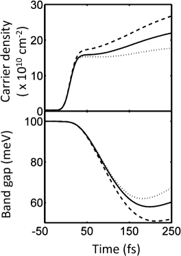
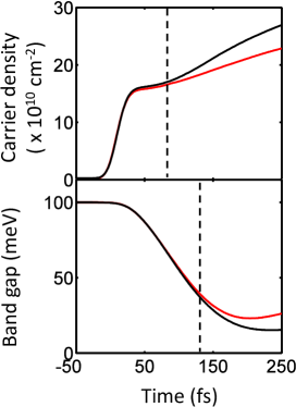
In Fig. 7 we compare different excitation photon energies, which lead to different energies at which the electrons are created in the conduction band. We call this the excitation energy and measure it from the unexcited Fermi energy , as sketched in Fig. 2. We analyze the cases of meV, 200 meV (which has been used so far and constitutes our reference setup in the following) and 250 meV. For the setup with meV, carriers are excited around 200 meV above the conduction-band bottom; the distance to the band bottom is reduced to 100 meV for the setup with meV. As shown in Fig. 7(top) the carrier density created during the optical pulse in the conduction band is only slightly different for the three setups, but its subsequent time evolution is different. However, the corresponding band gap changes for the different excitation energies in Fig. 7(bottom) deviate only by around 20 meV, i.e., 10 meV for each band, which is much smaller than the difference of the excitation energies. The most important contribution to the difference in carrier densities for the three excitation energies must therefore be due to different carrier multiplication effects, and the impact ionization is most efficient for the setup with meV. Fig. 7 further shows that the efficiency of the mutual amplification between impact ionization and gap closing increases nonlinearly. After 250 fs the values for the the carrier multiplication are 73%, 42% and 14%, respectively, for the excitation energies of meV, 200 meV and 150 meV. The corresponding band gaps are 52 meV, 60 meV, and 67 meV. This nonlinearity is mainly due to repeated interband scattering processes that become possible for electrons excited at higher energies. During their scattering dynamics toward the band bottom these electrons can contribute to the carrier multiplication process twice or more times.
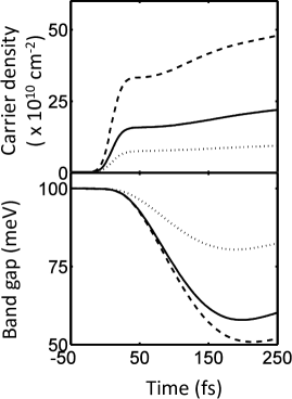
In Fig. 8 we investigate the dependence of the dynamics on the excitation strength. We compare three amplitudes of the Rabi energy : 6.6 meV, 10.0 meV (our reference setup and the value used so far) and 15.0 meV. In difference to Fig. 7, the carrier density created in the conduction band by the optical excitation is different for the three cases. The carrier density is the driving force of the coherent-phonon amplitude, which induces an atomic displacement responsible for the band gap dynamics, so that we obtain a higher initial band gap reduction for larger values of and this band gap remains smaller due to the mutual amplification between gap closing and impact ionization. The gap closing evidently saturates in Fig. 8(bottom). The effect of impact ionization can be assessed from the carrier multiplication in Fig. 8(top), which is 33%, 42% and 43%, respectively for Rabi energies meV, 10.0 meV and 15 meV. This carrier multiplication shows only a comparatively small increase between the two smaller Rabi energies whereas we have a pronounced difference in the gap closing. The difference between the dynamical scenarios shown in Fig. 8 is therefore mainly due to the different gap closing related to the initial photoexcited carrier density and the saturation of the gap closing is mainly responsible for the saturation of the carrier multiplication. Parenthetically we remark that a saturation of the gap quenching of the charge-density wave state has been observed in the charge-density wave material RTe3 where only an incomplete suppression of the charge-density wave occurs; here, we find an indication of a saturation for comparatively small electron-phonon coupling. Rettig et al. (2016)
IV.3 Influence of different band shapes
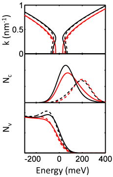
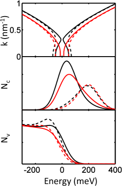
As already mentioned, we are interested in elucidating the influence of the band structure on measurable quantities, in particular energy distribution curves produced by photoemission experiments. In order to understand the calculated broadened distribution functions that can be compared with experiment, we here first discuss the influence of the band shape on the carrier dynamics without added broadening, and use for the comparison a parabolic band and the Mexican hat shaped band that we have based our calculations on so far. For a meaningful comparison, we define the parabolic band setup using all band parameters of the Mexican-hat like band setup, except a change of the on-site energies and from eV to eV. In this way, the parabolic and the Mexican-hat shaped bands have the same band gap, but in the parabolic case it occurs at and in the Mexican-hat band case at . The band structures are plotted in Figs. 11(top) and 12(top) as dotted lines.
In Fig. 9 and Fig. 10 the gap closing and carrier density in the conduction band vs. time is shown for the parabolic and Mexican-hat shaped band structures with meV and meV, respectively. Due to the different band shape, the ”tuning” of the band dispersion and the optical excitation is slightly different. We have already seen in Fig. 7 that such a small difference in excitation energy will also lead to a slightly different optically excited carrier density for the two band structures. However, the further time evolution of the carrier density is mainly determined by the different band dispersions. The origin of the steeper band dispersion for the Mexican-hat shaped band is the characteristic band gap minimum at a (i.e., not at the high-symmetry point), and a local band gap maximum at (the high symmetry point) in contrast to the parabolic case, where the global band gap minimum is at . The efficiency of the impact ionization depends on the size of the band gap and the -dependent Bloch wavefunctions, which include band mixing effects, as well as the available phase space for the scattering process. The band mixing is connected to the position of the band gap minimum and, thus, different between the parabolic and Mexican-hat setups.
These qualitative differences between the band structures should lead to different carrier dynamics, and we compare these dynamics in Figs. 9–12. In a parabolic band, the hot carriers relax directly into the high symmetry point, while in the case of the Mexican-hat shaped band, hot carriers relax more into the band minimum and reach the local maximum at the high symmetry point only with a delay. Therefore, band gap minima on different positions combined with a different dependence of the available phase space results in different efficiency for impact ionization for equal band gap minima. We first focus on Figs. 9 and Fig. 10 where we compare the gap closing and conduction-band carrier density between Mexican-hat and parabolic bands for different electron-phonon couplings. A higher impact ionization efficiency for the Mexican-hat shaped band induces a difference in the carrier density between the two band structures, as can be seen from splitting of the curves above 100 fs in Figs. 9 and Fig. 10, respectively. The mutual amplification between impact ionization and band gap closing amplifies the difference in the temporal evolution of the band gap (see splitting of the curves at a slightly later time around 150 fs) and of the impact ionization efficiency. Therefore, the difference between the two band structures increases for band gap and conduction-band carrier density with time. In Fig. 9 this results in a band gap of 60 meV and 62 meV and a carrier multiplication of 42% and 35% (factor: 1.2) for the Mexican-hat structures compared to the respective calculation with the parabolic bands. In Fig. 10 for the larger electron-phonon coupling meV we have band gaps of 15 meV and 26 meV after 250 fs, and carrier multiplications of 74% and 50% (factor: 1.5) for the Mexican-hat and parabolic bands, respectively. Depending on the electron-phonon matrix element the influence of the band shape can therefore be substantial.
In Figs. 11 and 12 we compare the time evolution of the band structure and broadened carrier distributions for the Mexican-hat and parabolic bands. As the broadened distributions average over all states in a given energy range set by in Eq. (17) they are influenced both by the carrier redistribution dynamics (i.e., carrier multiplication) and by the band structure, especially if the band structure changes. In our earlier paper, Mathias et al. (2016) we presented a simple parabolic model without band mixing and without a dynamically changing band structure. With the present calculation for parabolic and Mexican-hat shaped bands and a consistent inclusion of band mixing effects, we can investigate the contribution of the dynamical band structure to the electron distribution curves.
Fig. 11 and Fig. 12 are for different electron-phonon couplings and are obtained from the same dynamical calculations as Figs. 9 and 10, respectively. For a broadening that corresponds to state-of-the-art photoemission experiments, the broadened carrier distributions created by the optical excitation around 25 fs are similar for the Mexican hat and parabolic bands, but a difference of the weighted carrier distribution in the conduction band can be seen after 250 fs. In the parabolic-band case, there are only rigid band shifts and negligible changes in band curvature so that the change in the broadened distribution reflects essentially only the redistribution by scattering processes and the increase in the number of carriers due to carrier multiplication. In the Mexican-hat band structure, there are pronounced changes in the band curvature that also influence the broadened distribution functions. While there are quantitative differences to the parabolic case, we observe a similar behavior of the broadened distribution function that is in qualitative agreement with the carrier multiplication factors determined from Figs. 9 and 10. We conclude that the behavior of computed broadened distribution functions, which are the quantity we compare to experimental electron-distribution curves and which are similar to experimental results on TiSe2, are an unambiguous indicator of carrier multiplication. The energy dependent signatures found in Figs. 11 and 12 are only influenced to a small extent by changes in the spectral properties of the carriers, even though the dynamical changes in the curvature of the Mexican hat band structure model likely overestimates those occurring in a real small-band gap material.
In the valence band, a characteristic bump below the Fermi energy appears only in the broadened distribution function in the Mexican-hat shaped band. The erosion of this bump, which is not visible in the parabolic band, indicates the effect of carrier multiplication. In TiSe2 the Se 4p band, as opposed to the Ti 3d, does not show a Mexican hat-like structure and therefore it is difficult to observe characteristics of impact ionization in the valence band with the energy broadening introduced by current experimental photoemission setups. Because the temporal evolution of the valence band signal is more influenced by the band and less influenced by the carrier dynamics, the difference between different band shapes, in particular in Fig. 11, is more pronounced than the differences between the two snapshots at different times.
V Conclusion
We investigated carrier multiplication dynamics due to impact ionization after ultrafast optical excitation in a model band structure of a quasi-two dimensional material with small band gaps. The photo-induced band gap narrowing close to the Fermi surface is incorporated using the coupling to coherent phonons, which mimics the quenching of an insulator phase. We used a dynamical approach that includes time-dependent band-energies and wave-functions, which make the Coulomb-matrix elements and the static screening effectively time-dependent. Using this model, we were able to quantify the contribution of impact ionization in the ultrafast response of small band-gap 2D materials and discussed the importance of the interplay between carrier and band dynamics. We computed broadened distribution functions that can be compared to energy distribution curves as they are measured in time-dependent photoemission spectroscopy, and we discussed the signatures of impact ionization and gap closing in these curves. We also investigated the influence dynamical changes in the band curvature, as these changes will also influence energy distribution curves and cannot, at present experimental resolutions, be distinguished from carrier multiplication effects. To this end, we compared a parabolic band structure with that of a Mexican hat and found that the characteristic change in energy distribution curves in, e.g., TiSe2, Mathias et al. (2016) are indeed mainly due to carrier multiplication effects, and only to a small extent due to changes in the spectral function of the electrons. Our computed energy dependent distribution curves compare well with experiments on TiSe2 and, even though we consider a specific coupling mechanism to a coherent phonon, we believe that our results capture a general trend in small band-gap 2D materials.
Appendix A Tight-binding model
For our tight-binding model we assume a quasi-two dimensional material like TMDCs with two kind of atoms Ad and Ap. In the case of a TMDC, atom sort Ad would be the transition metal atom (e.g. Ti) with d-type or f-type valence orbital and atom sort Ap would be the chalcogen atoms (e.g. Se) with p-type valence orbitals. The unit cell would consist of one Ad and two Ap atoms. For example the lattice vectors , and would span a unit cell with the atom basis for Ad, for the first Ap and for the second Ap. The nearest-neighboring Ad or Ap atoms in the same plane would have a hexagonal or tetragonal symmetry. To model an accurate bandstructure for a TMDC around the Fermi surface the three (i.e. , , ) and eventually the energetically higher two (i.e. , ) orbitals of the atom of sort Ad and the six p-orbitals of the two atoms of sort Ap might be considered.Van Wezel et al. (2010)
Weak interactions between neighboring orbitals are usually neglected and the remaining interactions are expressed in terms of Slater-Koster integrals.Slater and Koster (1954) The bond integrals between two orbitals are distinguished between , or eventually bondings. For example, as described in Ref. van Wezel et al., 2010; Van Wezel et al., 2010 for TiSe2, only the three hopping pathways ddσ, ppσ and pdπ contribute significantly to the behavior of charges close to the Fermi energy. The resulting band structure around the high symmetry points under investigation of the small band-gap TMDCs is often highly un-isotropic like in TiSe2 as reported, e.g., in Ref. Monney et al., 2010. For this material, the non-isotropic band dispersion of the Ti 3d band is non-parabolic, i.e., an ellipsoid, and has a Mexican-hat shape geometry in the CDW insulator phase.
Regarding the investigated band dynamics of such a material in the insulator phase, we avoid a material realistic description, where the insulator phase is determined from the normal phase, to investigate the role of different kinds of interactions in the phase transition. Instead we model the TB Hamiltonian already in the insulator phase and describe the band dynamics via an effective atomic displacement as disturbance of the insulator phase. To model the small band-gap around the fermi surface, we use a simple two-band tight-binding model capable to describe the characteristics of the carrier and band-dynamics of such a material after an ultrashort optical excitation. Thus, we obtain an isotropic band-shape around a high symmetry point. The validity of this assumption is additionally motivated at the end of this section.
To transform a more material-realistic TB model into a simpler model with high symmetry capable to describe the characteristics of the carrier and band-dynamics close to the important high-symmetry point, a lot of more or less sophisticated transformation can be done. A simple way of doing it, is to disregard the and to consider only one orbital, e.g., , of Ad and one orbital, e.g., , of Ap and give only , and finite values. In the spirit of such a transformation, we use the following effective tight-binding hamiltonian to describe the investigated small band-gap insulator phase
| (18) |
where , are the on-site energies, , , are the tight-binding coupling-elements and is the relative distance vector between the two effective atoms within the unit cell. As we do not include spin-orbit coupling, we do not explicitly write out the spin-dependence in the following. The outcome is a conduction band mainly originating from a d-type transition metal orbital and a valence band mainly originating from a p-type chalcogen orbital. In the region of the examined high symmetry point, we obtain a angular symmetric Mexican-hat shaped band with a small band gap and a high band mixing. However, assuming a fast angular redistribution of carrier via electron-phonon scattering as e.g. reported in Ref. Mittendorff et al., 2014, the fundamental results of this investigation are also transferable to non-parabolic band structures.
Appendix B Equation-of-motion in the time-dependent eigenbasis
We start from the total Hamiltonian
| (19) |
consisting of a quasi-particle hamiltonian and an interaction hamiltonian . If the quasi-particle part is time-dependent, as discussed in section II.2, where , the eigenvalues and eigenvectors of this Hamiltonian have to be calculated for every time-step of the dynamical calculation. Such a time-dependent basis is associated with a basis transformation of the whole equation of motion for every time step as discussed in the following.
We start using the eigenbasis of quasi-particle hamiltonian at a time . In this basis the equation of motion for the reduced density matrix is
| (20) |
The quasi-particle part of the equation-of-motion can be written as
| (21) |
and the interaction part can be written in the general form of
| (22) |
i.e. a sum over correlation contributions , which are functionals of the density matrices .
For a time , the equation of motion in the new eigenbasis of the system at time takes the form
| (23) |
where is a unitary matrix of the basis transformation between the eigenbasis at the time and the eigenbasis at the time . For the quasi-particle part we obtain
| (24) |
The transformation of the interaction part can be done in an analogous fashion, but the derivation depends on the level of approximation employed for the interaction. We assume here that the interaction part can finally be written in a general form as
| (25) |
One advantage of such a basis transformation is that can be interpreted as the occupation of the state at time . Therefore, the intuitive physical picture used in common approximation schemes is preserved. However, the basis transformation is associated with a transformation of diagonal density-contributions into off-diagonal coherence-contributions in conjunction with correlated correction-terms in the equation-of-motion as shown above.
In the case of a sufficiently strong dephasing of the coherences, the off-diagonal contributions in conjunction with the correction from the correlation contribution can be neglected in the equation of motion. Then, the carrier occupation adapts instantaneously to the new band structure. We assume that the composition of the bands does not change too fast and approximate the result of this adaptation to be . We thus implement the time-dependent basis in the description of the carrier dynamics using time-dependent band-energies and wave-functions including time-dependent Coulomb-matrix elements due to the basis transformation with a time-dependent screening. The band dynamics here lead to an additional re-distribution of carriers into the new equilibrium distribution and a different pronunciation of intra- and inter-band scattering pathways.
For example the Coulomb scattering terms for the occupation at time can be written as
| (26) |
with
| (27) | |||||
| (28) | |||||
| (29) | |||||
| (30) |
References
- Rohwer et al. (2011) T. Rohwer, S. Hellmann, M. Wiesenmayer, C. Sohrt, A. Stange, B. Slomski, A. Carr, Y. Liu, L. M. Avila, M. Kalläne, et al., Nature 471, 490 (2011), ISSN 0028-0836, URL http://www.nature.com/doifinder/10.1038/nature09829.
- Sobota et al. (2014) J. A. Sobota, S. L. Yang, D. Leuenberger, A. F. Kemper, J. G. Analytis, I. R. Fisher, P. S. Kirchmann, T. P. Devereaux, and Z. X. Shen, Journal of Electron Spectroscopy and Related Phenomena 195, 249 (2014), ISSN 03682048, eprint 1401.3078, URL http://dx.doi.org/10.1016/j.elspec.2014.01.005.
- Eich et al. (2014) S. Eich, A. Stange, A. V. Carr, J. Urbancic, T. Popmintchev, M. Wiesenmayer, K. Jansen, A. Ruffing, S. Jakobs, T. Rohwer, et al., Journal of Electron Spectroscopy and Related Phenomena 195, 231 (2014), ISSN 03682048, URL http://dx.doi.org/10.1016/j.elspec.2014.04.013.
- Smallwood et al. (2016) C. L. Smallwood, R. A. Kaindl, and A. Lanzara, EPL (Europhysics Letters) 115, 27001 (2016), ISSN 0295-5075, eprint 1610.00202, URL http://stacks.iop.org/0295-5075/115/i=2/a=27001?key=crossref.fc96d0688dcc85d1c7738f1d4cc5a942.
- Gierz (2017) I. Gierz, Journal of Electron Spectroscopy and Related Phenomena 219, 53 (2017), ISSN 0368-2048, URL http://www.sciencedirect.com/science/article/pii/S0368204816301657.
- Gierz et al. (2013) I. Gierz, J. C. Petersen, M. Mitrano, C. Cacho, E. Turcu, E. Springate, A. Stöhr, A. Köhler, U. Starke, and A. Cavalleri, Nature Materials 12, 1119 (2013), ISSN 1476-1122, eprint 1304.1389, URL http://arxiv.org/abs/1304.1389{%}0Ahttp://dx.doi.org/10.1038/nmat3757.
- Stroucken et al. (2013) T. Stroucken, J. H. Grönqvist, and S. W. Koch, Phys. Rev. B 87, 245428 (2013), URL https://link.aps.org/doi/10.1103/PhysRevB.87.245428.
- Mihnev et al. (2016) M. T. Mihnev, F. Kadi, C. J. Divin, T. Winzer, S. Lee, C.-H. Liu, Z. Zhong, C. Berger, W. A. de Heer, E. Malic, et al., Nat. Commun. 7, 11617 (2016), ISSN 2041-1723, URL http://www.nature.com/doifinder/10.1038/ncomms11617.
- Kadi et al. (2015) F. Kadi, T. Winzer, A. Knorr, and E. Malic, Scientific Reports 5, 16841 (2015), ISSN 2045-2322, eprint 1508.06783, URL http://arxiv.org/abs/1508.06783{%}0Ahttp://dx.doi.org/10.1038/srep16841.
- Bhimanapati et al. (2015) G. R. Bhimanapati, Z. Lin, V. Meunier, Y. Jung, J. Cha, S. Das, D. Xiao, Y. Son, M. S. Strano, V. R. Cooper, et al., ACS Nano 9, 11509 (2015), ISSN 1936086X.
- Chhowalla et al. (2013) M. Chhowalla, H. S. Shin, G. Eda, L.-J. Li, K. P. Loh, and H. Zhang, Nature Chemistry 5, 263 (2013), ISSN 1755-4330, eprint 1205.1822, URL http://www.nature.com/doifinder/10.1038/nchem.1589.
- Voiry et al. (2015) D. Voiry, A. Mohite, and M. Chhowalla, Chem. Soc. Rev. 44, 2702 (2015), ISSN 0306-0012, URL http://xlink.rsc.org/?DOI=C5CS00151J.
- Steinhoff et al. (2016) A. Steinhoff, M. Florian, M. Rösner, M. Lorke, T. O. Wehling, C. Gies, and F. Jahnke, 2D Materials 3, 031006 (2016), URL http://stacks.iop.org/2053-1583/3/i=3/a=031006.
- Hellmann et al. (2012) S. Hellmann, T. Rohwer, M. Kalläne, K. Hanff, C. Sohrt, A. Stange, A. Carr, M. Murnane, H. Kapteyn, L. Kipp, et al., Nat. Commun. 3, 1069 (2012), ISSN 2041-1723, URL http://www.nature.com/doifinder/10.1038/ncomms2078.
- Ghatak et al. (2011) S. Ghatak, A. N. Pal, and A. Ghosh, Acs Nano 5, 7707 (2011).
- Cheiwchanchamnangij and Lambrecht (2012) T. Cheiwchanchamnangij and W. R. Lambrecht, Phys. Rev. B 85, 205302 (2012).
- Chernikov et al. (2015) A. Chernikov, C. Ruppert, H. M. Hill, A. F. Rigosi, and T. F. Heinz, Nature Photonics 9, 466 (2015).
- Chen et al. (2016) H. Chen, X. Wen, J. Zhang, T. Wu, Y. Gong, X. Zhang, J. Yuan, C. Yi, J. Lou, P. M. Ajayan, et al., Nat. Commun. 7, 12512 (2016).
- Steinhoff et al. (2017) A. Steinhoff, M. Florian, M. Rösner, G. Schönhoff, T. O. Wehling, and F. Jahnke, Nature communications 8, 1166 (2017).
- Moon et al. (2018) B. H. Moon, J. J. Bae, M.-K. Joo, H. Choi, G. H. Han, H. Lim, and Y. H. Lee, Nat. Commun. 9, 2052 (2018).
- Grüner (1988) G. Grüner, Reviews of Modern Physics 60, 1129 (1988), ISSN 00346861.
- Zhu et al. (2015) X. Zhu, Y. Cao, J. Zhang, E. W. Plummer, and J. Guo, Proceedings of the National Academy of Sciences 112, 2367 (2015), ISSN 0027-8424, eprint 1503.01858, URL http://www.pnas.org/lookup/doi/10.1073/pnas.1424791112.
- Flicker and Van Wezel (2015) F. Flicker and J. Van Wezel, Nat. Commun. 6, 7034 (2015), ISSN 2041-1723, eprint 1502.06816, URL http://www.nature.com/doifinder/10.1038/ncomms8034.
- Cho et al. (2016) D.-N. Cho, J. van den Brink, H. Fehske, K. W. Becker, and S. Sykora, Scientific Reports 6, 22548 (2016), ISSN 2045-2322, eprint 1603.01157, URL http://www.nature.com/articles/srep22548.
- Leroux et al. (2018) M. Leroux, L. Cario, A. Bosak, and P. Rodière, Phys. Rev. B 97, 195140 (2018).
- Nakata et al. (2018) Y. Nakata, K. Sugawara, S. Ichinokura, Y. Okada, T. Hitosugi, T. Koretsune, K. Ueno, S. Hasegawa, T. Takahashi, and T. Sato, npj 2D Materials and Applications 2, 12 (2018).
- Wall et al. (2012) S. Wall, D. Wegkamp, L. Foglia, K. Appavoo, J. Nag, R. Haglund, J. Stähler, and M. Wolf, Nat. Commun. 3, 721 (2012), ISSN 2041-1723, eprint 1012.1468, URL http://www.nature.com/doifinder/10.1038/ncomms1719.
- Mizokawa et al. (2009) T. Mizokawa, K. Takubo, T. Sudayama, Y. Wakisaka, N. Takubo, K. Miyano, N. Matsumoto, S. Nagata, T. Katayama, M. Nohara, et al., Journal of Superconductivity and Novel Magnetism 22, 67 (2009).
- Sykora et al. (2009) S. Sykora, A. Huebsch, and K. W. Becker, EPL (Europhysics Letters) 85, 57003 (2009).
- Kim et al. (2015) S. Kim, K. Kim, and B. I. Min, Scientific Reports 5, 15052 (2015), ISSN 2045-2322, URL http://www.nature.com/articles/srep15052.
- Ritschel et al. (2015) T. Ritschel, J. Trinckauf, K. Koepernik, B. Büchner, M. v. Zimmermann, H. Berger, Y. I. Joe, P. Abbamonte, and J. Geck, Nature Physics 11, 328 (2015), ISSN 1745-2473, eprint 1409.7341, URL http://www.nature.com/doifinder/10.1038/nphys3267.
- Gu and Rondinelli (2016) M. Gu and J. M. Rondinelli, Scientific Reports 6, 25121 (2016), ISSN 2045-2322, URL http://www.nature.com/articles/srep25121.
- Khitun et al. (2016) A. Khitun, G. Liu, and A. A. Balandin, arXiv preprint arXiv:1612.00028 (2016).
- Rossnagel (2011) K. Rossnagel, Journal of Physics: Condensed Matter 23, 213001 (2011).
- Porer et al. (2014) M. Porer, U. Leierseder, J.-M. Ménard, H. Dachraoui, L. Mouchliadis, I. E. Perakis, U. Heinzmann, J. Demsar, K. Rossnagel, and R. Huber, Nature Materials 13, 857 (2014), ISSN 1476-1122, URL http://www.nature.com/doifinder/10.1038/nmat4042.
- Zhang et al. (2018) K.-W. Zhang, C.-L. Yang, B. Lei, P. Lu, X.-B. Li, Z.-Y. Jia, Y.-H. Song, J. Sun, X. Chen, J.-X. Li, et al., Science Bulletin 63, 426 (2018).
- Monney et al. (2009) C. Monney, H. Cercellier, F. Clerc, C. Battaglia, E. F. Schwier, C. Didiot, M. G. Garnier, H. Beck, P. Aebi, H. Berger, et al., Phys. Rev. B 79, 045116 (2009), URL https://link.aps.org/doi/10.1103/PhysRevB.79.045116.
- Monney et al. (2010) C. Monney, E. F. Schwier, M. G. Garnier, N. Mariotti, C. Didiot, H. Beck, P. Aebi, H. Cercellier, J. Marcus, C. Battaglia, et al., Phys. Rev. B 81, 155104 (2010), URL https://link.aps.org/doi/10.1103/PhysRevB.81.155104.
- Cazzaniga et al. (2012) M. Cazzaniga, H. Cercellier, M. Holzmann, C. Monney, P. Aebi, G. Onida, and V. Olevano, Phys. Rev. B 85, 195111 (2012), URL https://link.aps.org/doi/10.1103/PhysRevB.85.195111.
- Monney et al. (2012a) C. Monney, G. Monney, P. Aebi, and H. Beck, Phys. Rev. B 85, 235150 (2012a), URL https://link.aps.org/doi/10.1103/PhysRevB.85.235150.
- Li et al. (2007) G. Li, W. Z. Hu, D. Qian, D. Hsieh, M. Z. Hasan, E. Morosan, R. J. Cava, and N. L. Wang, Phys. Rev. Lett. 99, 027404 (2007), URL https://link.aps.org/doi/10.1103/PhysRevLett.99.027404.
- Monney et al. (2011) C. Monney, C. Battaglia, H. Cercellier, P. Aebi, and H. Beck, Phys. Rev. Lett. 106, 106404 (2011), URL https://link.aps.org/doi/10.1103/PhysRevLett.106.106404.
- Kogar et al. (2017) A. Kogar, M. S. Rak, S. Vig, A. A. Husain, F. Flicker, Y. I. Joe, L. Venema, G. J. MacDougall, T. C. Chiang, E. Fradkin, et al., Science 358, 1314 (2017).
- Chen et al. (2017) C. Chen, B. Singh, H. Lin, and V. M. Pereira, arXiv preprint arXiv:1712.04967 (2017).
- Pasquier and Yazyev (2018) D. Pasquier and O. V. Yazyev, arXiv preprint arXiv:1805.11560 (2018).
- Golež et al. (2016) D. Golež, P. Werner, and M. Eckstein, Phys. Rev. B 94, 035121 (2016).
- Rossnagel et al. (2002) K. Rossnagel, L. Kipp, and M. Skibowski, Phys. Rev. B 65, 235101 (2002), URL https://link.aps.org/doi/10.1103/PhysRevB.65.235101.
- Karam et al. (2018) T. E. Karam, J. Hu, and G. A. Blake, ACS Photonics 5, 1228 (2018).
- Hughes (1977) H. P. Hughes, Journal of Physics C: Solid State Physics 10, L319 (1977).
- Hellgren et al. (2017) M. Hellgren, J. Baima, R. Bianco, M. Calandra, F. Mauri, and L. Wirtz, Phys. Rev. Lett. 119, 176401 (2017).
- Kidd et al. (2002) T. E. Kidd, T. Miller, M. Y. Chou, and T.-C. Chiang, Phys. Rev. Lett. 88, 226402 (2002), URL https://link.aps.org/doi/10.1103/PhysRevLett.88.226402.
- van Wezel et al. (2010) J. van Wezel, P. Nahai-Williamson, and S. S. Saxena, Physica Status Solidi (B) 247, 592 (2010), ISSN 03701972.
- Monney et al. (2012b) C. Monney, G. Monney, P. Aebi, and H. Beck, New Journal of Physics 14, 075026 (2012b), ISSN 1367-2630, URL http://stacks.iop.org/1367-2630/14/i=7/a=075026?key=crossref.020eee40fac0dd1e0eb2c27c6c8aa015.
- Van Wezel et al. (2010) J. Van Wezel, P. Nahai-Williamson, and S. S. Saxena, Phys. Rev. B 81, 165109 (2010), URL https://link.aps.org/doi/10.1103/PhysRevB.81.165109.
- Phan et al. (2013) V.-N. Phan, K. W. Becker, and H. Fehske, Phys. Rev. B 88, 205123 (2013), URL https://link.aps.org/doi/10.1103/PhysRevB.88.205123.
- Watanabe et al. (2015) H. Watanabe, K. Seki, and S. Yunoki, Phys. Rev. B 91, 205135 (2015), URL https://link.aps.org/doi/10.1103/PhysRevB.91.205135.
- Bianco et al. (2015) R. Bianco, M. Calandra, and F. Mauri, Phys. Rev. B 92, 094107 (2015), URL https://link.aps.org/doi/10.1103/PhysRevB.92.094107.
- Monney et al. (2016) C. Monney, M. Puppin, C. W. Nicholson, M. Hoesch, R. T. Chapman, E. Springate, H. Berger, A. Magrez, C. Cacho, R. Ernstorfer, et al., Phys. Rev. B 94, 165165 (2016), URL https://link.aps.org/doi/10.1103/PhysRevB.94.165165.
- Maschek et al. (2016) M. Maschek, S. Rosenkranz, R. Hott, R. Heid, M. Merz, D. Zocco, A. Said, A. Alatas, G. Karapetrov, S. Zhu, et al., Phys. Rev. B 94, 214507 (2016).
- Singh et al. (2017) B. Singh, C.-H. Hsu, W.-F. Tsai, V. M. Pereira, and H. Lin, Phys. Rev. B 95, 245136 (2017).
- Ishioka et al. (2010) J. Ishioka, Y. H. Liu, K. Shimatake, T. Kurosawa, K. Ichimura, Y. Toda, M. Oda, and S. Tanda, Phys. Rev. Lett. 105, 176401 (2010), URL https://link.aps.org/doi/10.1103/PhysRevLett.105.176401.
- Castellan et al. (2013) J.-P. Castellan, S. Rosenkranz, R. Osborn, Q. Li, K. E. Gray, X. Luo, U. Welp, G. Karapetrov, J. P. C. Ruff, and J. van Wezel, Phys. Rev. Lett. 110, 196404 (2013), URL https://link.aps.org/doi/10.1103/PhysRevLett.110.196404.
- Silva et al. (2018) A. Silva, J. Henke, and J. van Wezel, Phys. Rev. B 97, 045151 (2018).
- Hildebrand et al. (2018) B. Hildebrand, T. Jaouen, M.-L. Mottas, G. Monney, C. Barreteau, E. Giannini, D. Bowler, and P. Aebi, Phys. Rev. Lett. 120, 136404 (2018).
- Weber et al. (2011) F. Weber, S. Rosenkranz, J.-P. Castellan, R. Osborn, G. Karapetrov, R. Hott, R. Heid, K.-P. Bohnen, and A. Alatas, Phys. Rev. Lett. 107, 266401 (2011), URL https://link.aps.org/doi/10.1103/PhysRevLett.107.266401.
- Mathias et al. (2016) S. Mathias, S. Eich, J. Urbancic, S. Michael, A. V. Carr, S. Emmerich, A. Stange, T. Popmintchev, T. Rohwer, M. Wiesenmayer, et al., Nat. Commun. 7, 12902 (2016), ISSN 20411723.
- Mittendorff et al. (2014) M. Mittendorff, T. Winzer, E. Malic, A. Knorr, C. Berger, W. A. de Heer, H. Schneider, M. Helm, and S. Winnerl, Nano Letters 14, 1504 (2014).
- Donkov et al. (2009) A. Donkov, I. Eremin, J. Knolle, and M. M. Korshunov, J. Supercond. Nov. Magn. 22, 37 (2009).
- Chakraborty et al. (2012) B. Chakraborty, A. Bera, D. V. S. Muthu, S. Bhowmick, U. V. Waghmare, and A. K. Sood, Phys. Rev. B 85, 161403 (2012), URL https://link.aps.org/doi/10.1103/PhysRevB.85.161403.
- Rettig et al. (2016) L. Rettig, R. Cortés, J.-H. Chu, I. R. Fisher, F. Schmitt, R. G. Moore, Z.-X. Shen, P. S. Kirchmann, M. Wolf, and U. Bovensiepen, Nat. Commun. 7, 10459 (2016).
- Slater and Koster (1954) J. C. Slater and G. F. Koster, Phys. Rev. 94, 1498 (1954), URL https://link.aps.org/doi/10.1103/PhysRev.94.1498.