Quantum transport through 3D topological insulator PN junction under magnetic fields
Abstract
The 3D topological insulator (TI) PN junction under magnetic fields presents a novel transport property which is investigated both theoretically and numerically in this paper. Transport in this device can be tuned by the axial magnetic field. Specifically, the scattering coefficients between incoming and outgoing modes oscillate with axial magnetic flux at the harmonic form. In the condition of horizontal mirror symmetry, the initial phase of the harmonic oscillation is dependent on the parities of incoming and outgoing modes. This symmetry is broken when a vertical bias is applied which leads to a kinetic phase shift added to the initial phase. On the other hand, the amplitude of oscillation is suppressed by the surface disorder while it has no influence on the phase of oscillation. Furthermore, with the help of the vertical bias, a special (1,-2) 3D TI PN junction can be achieved, leading to a novel spin precession phenomenon.
I Introduction
Topological insulator (TI) is a sort of electronic materials which have insulating bulk states and conducting surface states protected by time-reversal symmetry.TI1 ; TI2 ; TI3 ; TI4 This conception was first proposed in 2D materialsHgTe and then generalized into 3D materials.predict1 ; predict2 ; predict3 The experimental realization of 3D TI was reported in several materials such as Bi1-xSbx,BiSb1 Bi2Te3,BiTe1 Sb2Te3LL4SbTe1 and Bi2Se3.BiSe1 ; BiSe2 With strong spin orbital coupling in 3D TI, the spin direction of surface state is constrained perpendicular to the momentum,modeth ; modet which is called spin-momentum locking and can be observed by angle-resolve photoemission spectroscopy (ARPES).mode0 Due to this spin-momentum locking property, an electron acquires Berry phase by going around the surface.ar1 ; zyf ; berry1 ; berry2 ; berry3 ; berry4 This phase can be compensated by a magnetic flux, leading an Aharonov-Bohm (AB) oscillation in conductance which has been observed in a number of experiments.AB1 ; AB2 ; AB3 ; AB4 With a strong magnetic field added perpendicular to the upper and lower surfaces, the energy spectrum of the upper and lower surfaces are reorganized into Landau-Level (LL),LL1 ; LL3 ; ar2 ; LJYin and the chiral modes emerge along the side surfacesar2 .
Tuning the potential on the two adjoint regions of a 3D TI ribbon by gate voltagegate1 ; gate2 ; gate3 or chemical dopingdoping1 , the 3D TI ribbon is turned into a 3D TI PN junction. Under perpendicular magnetic field, chiral modes come into being at the PN boundary and side surfaces.3dtipnj Based on the chiral modes, in 2015, a spin-based Mach-Zehnder interferometry has been proposed on this 3D TI PN junction with a strong vertical magnetic field and an axial magnetic flux.core The conductance in this device can be tuned with the magnetic flux which presents a harmonic oscillation. In addition, the spin polarization of the reflected and transmitted currents are opposite, which enables this device to work as a spin splitter.
In this paper, we take a thorough investigation in the transport property of 3D TI PN junction under magnetic field. The transport property is described by the scattering coefficients between the incoming and outgoing modes which are calculated by the Green’s function method. These scattering coefficients, as well as the conduction, oscillate with magnetic flux at the harmonic form. The initial phase of the oscillation is 0 or dependent on the parities of modes in the pristine 3D TI PN junction where the horizontal mirror symmetry is conserved and the parity is well defined. The symmetry is broken when a non-zero vertical bias is applied. This vertical bias changes the potential energy in both upper and lower surfaces, leading to a kinetic phase shift in the oscillation. In some cases, the vertical bias changes the number of modes and generates a special (1,-2) 3D TI PN junction, in which a novel spin precession phenomenon happens. We also investigate the effect of disorder on the lower surface in imitation of substrate. The phase shift of oscillation at every single disorder configuration is neutralized when it averages in a large configuration ensemble. Instead, the averaged conductance oscillation shows a suppression in amplitude.
The rest of this paper is organized as follow: In Sec.II we give the form of Hamiltonian and illustrate the modes which constitute the transport path. In Sec.III we introduce the scattering coefficient and give an overview of the conductance in different conditions. Sec.IV shows the parity effect on scattering coefficients in symmetric 3D TI PN junction. Sec.V shows the two effects of vertical bias: kinetic phase (Sec.V.1) and spin precession (Sec.V.2). Sec.VI presents the effect of disorder on the lower surface of 3D TI PN junction. Finally, we conclude the work in Sec.VII.
II model and modes
One of the scheme of 3D TI PN junction is shown in Fig.1(a), which is a square nanoribbon. Cartesian coordinate system is established of which the x axis is along the injecting direction of electrons and z is along the normal vector of the upper and lower surfaces. The original point is in the center of this 3D TI nanoribbon. The nanoribbon is divided into two regions by y-z plane: the entrance region in which electrons are injected, and the exit region. The potential of entrance region is tuned by gate voltage , while tunes the exit region. The perpendicular magnetic field is along the -z direction. Axial magnetic field generates a flux where and denote the length of y and z direction respectively. If the 3D TI PN junction is made by chemical doping, the upper and lower surfaces might be symmetric. However, in the scheme presented in Fig.1(a), the gates generate a perpendicular electrostatic field and lead to a vertical bias between upper and lower surfaces. Without loss of generality, we introduce a bias term to take this possible bias into consideration.
We adopt a lattice model to describe the surface of 3D TI PN junction. Although there exists a fermion doubling problem in the lattice model of 3D TI,double this trouble can be solved by introducing a Wilson term in the Hamiltonian.zyf The discretized lattice Hamiltonian of the surface of 3D TI PN junction iszyf
| (1) | |||||
where
| (2) |
The surface of the 3D TI PN nanoribbon is discretized into infinite layers along the direction and each layer is discretized into sites. The sites are labeled by , where and are integer with () being the layer index and and () being the index along the circumference of the 3D TI ribbon. and creates and annihilates an electron on site . and are the AB phases generated by perpendicular and axial magnetic fields, respectively. where denotes the y coordinate of site . In the following numerical calculation, is in units of , and we also take the lattice constant nm and the Fermi velocity m/s. This Fermi velocity corresponds to topological insulator and ,vfadd1 ; vfadd2 which can be experimentally extracted from ARPES and scanning tunneling spectroscopy (STS). The Wilson term factor which is brought in artificially to avoid fermion doubling problem. Without loss of generality, the electrostatic potential is a combination of , and : in the entrance region and in the exit region, where is the z coordinate of site . In particular, the potentials on the upper entrance, lower entrance, upper exit, and lower exit surfaces respectively are , , , and , with , , , and being the corresponding filling factors. Then and denote the filling factors in entrance () and exit () regions.
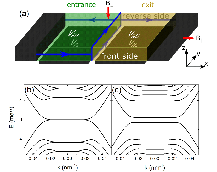
In this paper, we study the quantum transport through 3D TI PN junction, which requires the dimensions of the device smaller than the coherence length. As for 3D TI, the coherent length can be measured by Aharonov-Bohm oscillation. In Ref.[AB3, ], it gives the coherent length to be at 2K and at 50mK. For this reason, we focus on the PN junction with its width being hundreds of nanometers. The quantum transport path in 3D TI PN junction consists of two different kinds of modes, namely, longitudinal modes on side surfaces and transverse modes along the PN interface on upper and lower surfaces. Fig.1(a) sketchily illustrates the transporting route of an electron along the modes. Incident electrons along the longitudinal mode on the front side surface arrive at the PN interface and then split into two branches of transverse modes going along the upper and lower PN boundaries respectively. The two branches converge at the reverse side surface with different phase which determines whether it will be scattered into forward or backward outgoing mode.
The longitudinal modes are the eigenstates of the 3D TI perfect nanoribbon. For a 3D TI perfect nanoribbon, there are four surfaces, i.e. the upper, lower, front side and reverse side surfaces. Here the upper and lower surfaces are much wider than the two side surfaces [see Fig.1(a)]. So the surfaces of the 3D TI ribbon can be viewed as two homogeneous surfaces (upper and lower surfaces) coupling by the narrow side surfaces. Away from the edges, the electrons in upper and lower surfaces are localized by the perpendicular magnetic field, corresponding to the double degenerate flat LLs in the middle of Fig.1(b). At the edges, the eigenstates in the upper and lower surfaces are coupled through the side surfaces, splitting into two branches in energy spectrum, which is in analogy with the bonding and anti-bonding states in molecule. The two branches derived from one LL hold different parity under horizontal mirror reflection [see Fig.5(a)]. This parity has an effect on the scattering coefficients which will be detailed in Sec.IV. The parity is broken under a nonzero vertical bias where each degenerate LL in upper and lower surfaces split into two LLs at a distance of [Fig.1(c)].
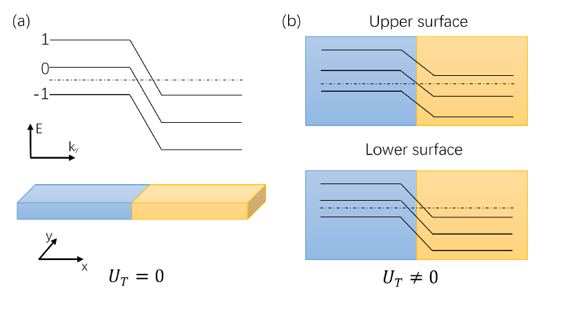
On the other hand, the transverse mode is derived from LLs in upper and lower surfaces [Fig.2(a)]. On the upper or lower surface of the 3D TI, the LLs are flat. However, these flat LLs are deformed near the PN interface, raising at one region and descending at the other region. If one LL crosses the Fermi level during this process, one transverse mode appears. Analytically, the number of transverse modes on the upper and lower surfaces respectively are and . In the absence of vertical bias (), the upper and lower surfaces are symmetric and their transverse modes are same also (). But when a nonzero vertical bias applied, this symmetry is broken and this may induce different number of transverse modes in some situations [Fig.2(b)].
Consider a 3D TI PN junction with the filling factor being in entrance region and in exit region [hereafter denoted as for simplicity]. There are incident longitudinal modes on the front side surface, and outgoing longitudinal modes on the reverse side surface, denoting backward modes in entrance region and denoting forward modes in exit region. The transverse modes on the upper and lower surfaces are denoted by and respectively, where and .
III conductance of 3D TI PN junction
In general, every incoming mode goes through the path in Fig.1(a) and is scattered into outgoing modes both backward and forward. We use the scattering coefficient to describe the possibility that an electron in mode is scattered into mode , namely,
| (3) |
The conservation of probability ensures that . The conductance of 3D TI PN junction is determined by the modes scattered forward, namely,
| (4) |
For the simplest case in a (1,-1) 3D TI PN junction where , the conductance has been proven harmonic oscillating with the axial magnetic flux .core The situation for multimodes is similar, since presents a same oscillation in the absence of (Sec.IV). The vertical bias induces a kinetic phase shift in scattering coefficient oscillation, which is discussed in Sec.V.1.
Based on the lattice Hamiltonian Eq.(1), the Green’s function method is applied to solve the scattering amplitude as well as conductance in 3D TI PN junction.my The detailed procedure (formula) for solving can refer Ref.[my, ]. The Green’s function method is flexible and available in different condition such as large filling factor, vertical bias, and disorder. In the numerical calculation, we set the perpendicular magnetic field Gs, the TI nanoribbon height nm and width nm, if not mentioned intentionally.
In Fig.3 and Fig.4, we give an overview of the conductance varying with gate voltage and under different axial magnetic flux and vertical bias . The conductance in (a) and (c) of both Fig.3 and Fig.4 is symmetric about diagonal, i.e. . Because of the current conservation in two-terminal system, the conductance is invariable when the PN junction rotates around z axis, which changes a junction into junction with changed into , so . When , we have as shown in Fig.3(a) and (c). In addition, conductance is the periodic function of axial magnetic flux with . When , , so in Fig.4(a) and (c). While the vertical bias , from Eqs.(4) and (6), one can obtain that the conductance is even function of regardless of other parameters.
In unipolar regime where and hold the same sign, the conductance presents several plateaus, since the conductance is dependent on the minimal channel number in the unipolar junction that . Specifically, when the upper and lower surfaces are symmetric and the LLs are doubly degenerate [Fig.1(b)]. Thus the conductance plateaus are odd number in units of in Fig.3. In Fig.4 as breaking the degeneracy of each LL [Fig.1(c)], the conductance plateau can occur at even number. In particular, there is a large light color cross with in the center of Fig.4(a) and (c), referring to the band gap induced by in Fig.1(c). In addition, from Fig.3 and Fig.4, one can see that the conductances at the first and third quadrant in panel (a) is almost the same as one in panel (c). This indicates little effect of the flux in unipolar regime.
On the other hand, in bipolar regime where and have the opposite sign, the conductance is strongly dependent on axial magnetic flux and vertical bias . From Fig.3 and Fig.4, the significant difference between (a) and (c) in the second and fourth quadrant shows the influence of in bipolar regime. When where upper and lower surfaces are symmetric, the conductance is quite small at [see Fig.3(a) and (b)], but it has the large value at [Fig.3(c) and (d)]. At , the conductance presents a plateau with the plateau value in and regimes [see Fig.3(d)]. While with a finite where the symmetry between the upper and lower surfaces is broken, the plateau disappears [see Fig.4(b) and (d)]. Now can be large at and is small at .
IV symmetric 3D TI PN junction
In this section we investigate the pristine 3D TI PN junction without vertical bias and disorder. The influence of the axial magnetic flux in bipolar regime is investigated in Fig.5, where we numerically simulate the scattering coefficient by the Green’s function method. The mirror reflection symmetry about x-y plane is preserved and we can define the parity for longitudinal modes under the reflection operator ,
| (5) |
The parity of each branch of bands is distinguished by color in Fig.5(a).
In the appendix, we show that the scattering coefficient is in the form of
| (6) |
where . Eq.(6) indicates that all the scattering coefficients harmonically oscillate with the flux , and the initial phase is either 0 or , dependent on the parity factor . If the incoming mode and outgoing mode hold the same parity, the initial phase is 0 and arrives at the peak at . On the other hand, if and hold different parities, the initial phase is and at .
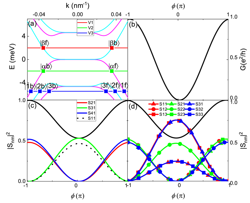
The scattering coefficients are divided into two parts by the outgoing index : those are reflection coefficients and are transmission coefficients. The conductance is the sum of all the transmission coefficients [see Eq.(4)]. The three candidate energy meV, meV and meV [see Fig.5(a)] are corresponding to three different filling factor , and . In the rest of this section, we repeatedly choose two of these candidate energies by choosing suitable and , to form various TI PN junctions and investigate the scattering coefficients varying with flux .
The PN junction is the most discussed case since it is in the lowest energy regime. There is only one transmission coefficient which is exactly proportional to the conductance. Fig.5(b) depicts the conductance . The is just the in Fig.5(a) and is . These two modes hold different parities. Thus and the initial phase is , leading that and it is at and at [see Fig.5(b)]. This also explains the and conductance plateaus in (1,-1) regime in Fig.3(b) and Fig.3(d).
In the PN junction, there are 3 forward outgoing modes , and , which are the state , and in Fig.5(a), with one incoming mode , which is just the , and one backward outgoing mode , which is just the . The parity of each mode gives and . Thus the initial phase are of and but 0 of and . Fig.5(c) shows the scattering coefficients , in which four exhibit the harmonic oscillations with and having the initial phase and and being the initial phase . Since the reflection coefficient at , the conductance is always 1 in units of . This accounts for the plateau in the (1,-3) regime in Fig.3(d).
The parity analysis also works in the multi-mode injecting case. In the (-3,1) PN junction there are three incoming modes which are the states in Fig.5(a), along with three backward modes which are the states . The nine reflection coefficients are depicted in Fig.5(d), distinguished by color and symbol of each curve. The color denotes the outgoing mode while the symbol denotes the incoming mode. It is clear that have the parity coefficient , and they have the maximum at and are zero at . The other four reflection coefficients have , leading that they are zero at and reach the maximum at [see Fig.5(d)]. Moreover, the combination of reflection about x-z plane and time reversion is conserved in this 3D TI PN junction, and this exchanges the and for . For this reason the reflection coefficients have the property . In addition, due to the current conservation in two-terminal system, the conductance of the (-3,1) PN junction is exactly equal to that of the (1,-3) PN junction [see Fig.5(c) and (d)].
V non-symmetric 3D TI PN junction in the nonzero vertical bias
The vertical bias breaks the symmetry of upper and lower surfaces and breaks the parity as well. The scattering coefficient is no more Eq.(6) but in a more general form (see appendix)
| (7) |
The initial phase is an arbitrary value instead of 0 or only. This phase shift is due to the momentum difference between transverse modes of upper and lower surfaces, which is called kinetic phase. In order to investigate these transverse modes, an infinite wide 3D TI PN junction is considered (i.e. the width ), and its energy spectrum is shown in Fig.6(a) and (c). From the energy spectrum, the transverse modes can be obtained from the intersection of the energy band and Fermi level.
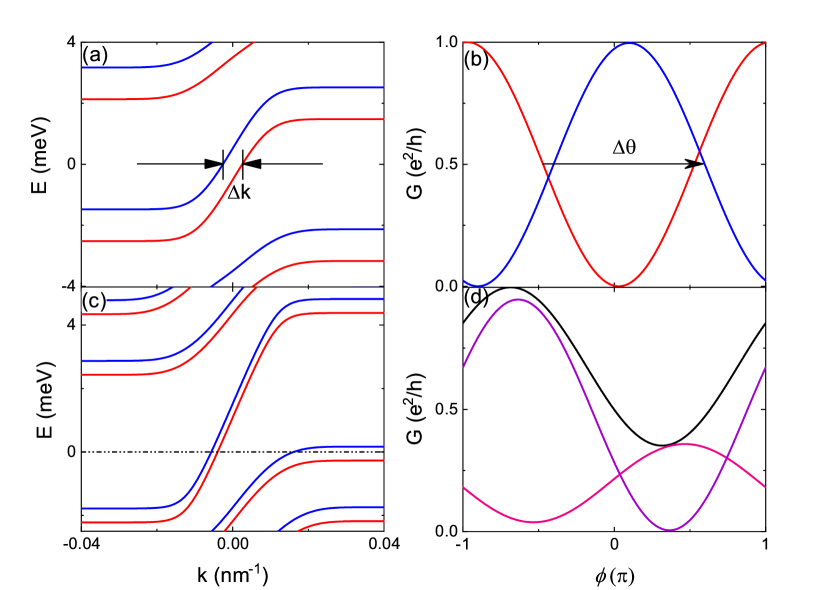
The transverse modes come from LLs which distort at the PN interface and cross the Fermi level. The vertical bias lifts the energy in upper surface by , and in lower surface. This leads to a momentum difference between upper and lower transverse modes [Fig.6(a)]. In a (1,-1) PN junction, this difference straightforwardly induces a kinetic phase shift in conductance oscillation [see Fig.6(b)]. The relation between and is detailed in Sec.V.1.
In some cases, creates a new crosspoint of LLs and Fermi level at one surface, inducing an additional transverse mode [Fig.6(c)]. This results in an even number of filling factor in the exit region for the sake of mode conservation. For this reason there are two transmission coefficients in total, which are depicted in Fig.6(d). The initial phase of each scattering coefficient is not restricted to 0 or , but an arbitrary value as in Eq.(7). This (1,-2) PN junction presents a novel spin precession phenomenon which is illuminated in Sec.V.2.
V.1 kinetic phase in (1,-1) TI PN junction
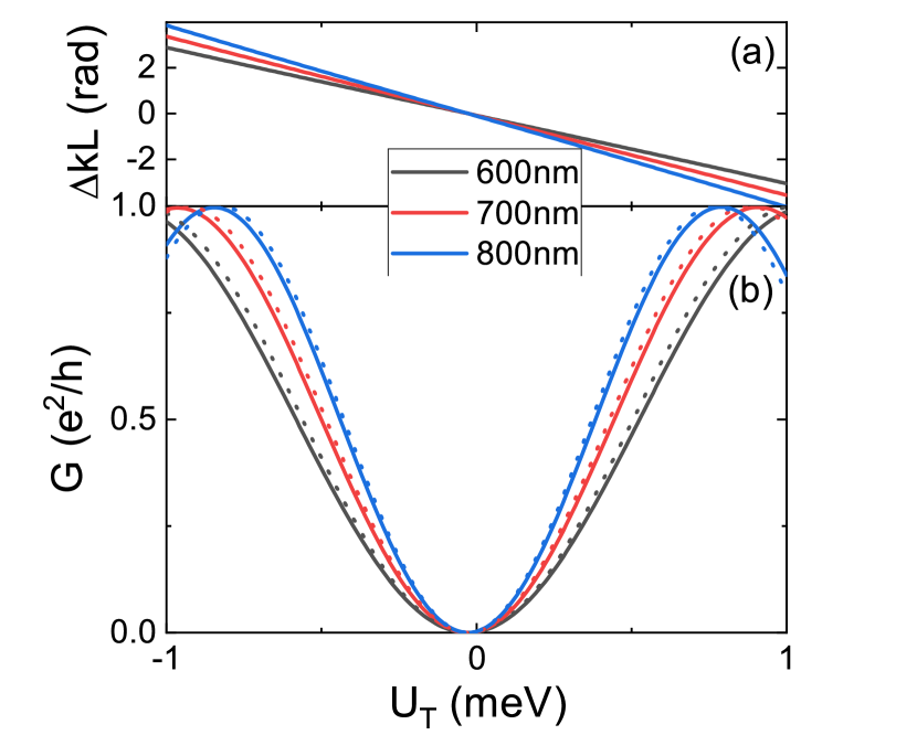
The kinetic phase shift in Fig.6(b) can be derived from Eq.(7). It gives the conductance in (1,-1) TI PN junction (see Appendix):
| (8) |
This deduction consists with our numerical results, see Fig.7. With the help of the infinite wide TI PN junction, the transverse modes and the momentum difference can be solved out directly by the transfer matrix method.my Then we can get the kinetic phase of every , as well as the analytical conductance in Eq.(8). Meanwhile, the conductance can numerically calculated by the Green’s function method. Fig.7(b) shows both analytical and numerical conductances for three different size of (1,-1) TI PN junctions as a comparison. Since is small compared with the scale of the energy band, it changes linearly. The kinetic phase varies proportionally to [see Fig.7(a)], causing a harmonic oscillation in conductance . Although the analytical is close enough to the numerical , there exists a small deviation, indicating the indeed phase shift is slightly lesser than the ideal kinetic phase . This might be attributed to the boundary effect, that the distance for transverse mode going through is not the full length of but the majority of it. This explanation also fits the fact that the deviation is small in long but large in short .
V.2 spin precession in (1,-2) TI PN junction
When the vertical bias , the (1,-2) TI PN junction is forbidden since the LLs are doubly degenerate and the filling factors are odd number. With the help of , (1,-2) TI PN junction is achieved and a novel spin precession appears. The spin polarization aligns along the side surfaces in the entrance region, but rotates along the reverse side surface in the exit region [see Fig.8(a)]. For the (1,-2) 3D TI PN junction, there exists an incoming mode on the front side surface, a reflecting mode and two transmitting modes and on the reverse side surface, and three transverse modes , and on the PN interface. The spin precession phenomenon is due to the interference of and , and it can be used in the spin valve devicesvalve .
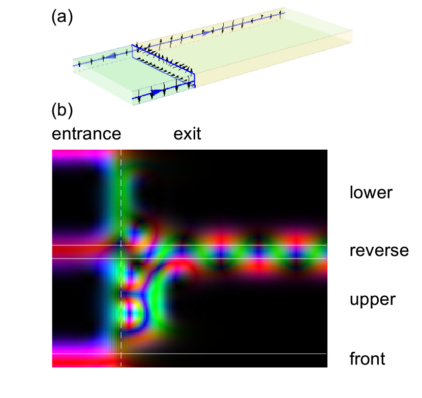
In order to illustrate the spin precession phenomenon, we simulate a sample of (1,-2) 3D TI PN junction of which the parameters are consistent with Fig.6(c), showing its spin distribution by expanded view in Fig.8(b). Spin polarization on the surface of 3D TI PN junction is described with the basis , with being along the x axis, being the normal direction of the surface, and being the tangential direction. The spin polarization is fixed on the front side and reverse side surfaces in the entrance region, as well along the transverse mode on the lower surface, since these areas contain only a single transmission mode. The wavefunction changes only at the overall phase factor by , which does not effect the value and direction of spin. In Fig.8(b), these areas with fixed polarization are presented monotonous in color. On the other hand, there presents complicated structures periodically arranged along the PN interface on the upper surface and on the reverse side surface in the exit region. These two areas are occupied by two different modes which interfere with each other producing a beat pattern, in which the spin precession occurs, i.e. the electron’s spin rotates as the electron moves ahead [see Fig.8(a)]. The spin precession originates from the two transmitting modes having different momentums. The beat in the exit region appears only at , because more than two different frequencies mixed together would break the periodical beat pattern.
The wavefunction in the exit region is
| (9) |
As shown in Fig.6(d), the transmission coefficients and vary with the axial magnetic flux . However, the space period of the spin precession is unrelated to . It is decided directly by the momentums of the two transmitting modes, and ,
| (10) |
These momentums are dependent on the energy spectrum of exit region which can be tuned by gate voltage and the magnetic field . Fig.9(c) shows that the space period of the spin precession increases with the gate voltage and decreases with the magnetic field .
Considering an electron moves ahead in the reverse side in exit region, its spin polarization vector rotates along a trajectory in the spin space of [See Fig.9(a)]. This trajectory is a closed orbit because of the periodicity. Because of spin-momentum locking, for , this means that the axial spin component is zero for every single longitudinal mode.core But the cross term . By using the wavefunction in Eq.(9), the spin polarization vector can be obtained that the orbit is always an ellipse of which the longer axis is parallel to . We introduce an opening angle of this longer axis to the ordinate origin to denote the changes of the spin direction in a spin precession period. This opening angle is influenced by magnetic flux [See Fig.9(b)] and is numerically analyzed in Fig.9(d). The flux goes through a cycle from to , and the plane of orbit passes the ordinate origin twice in the cycle, forming two peaks in curve versus in Fig.9(d). At the peaks, can almost reach the largest value . With the change of the system’s parameters, these two peaks with the large can usually exist. Notice that a large opening angle in the spin precession is very conducive to spin valve devices.
VI effect of disorder on the transport through TI PN junction
In practice, the symmetry of upper and lower surfaces is often broken even without vertical bias. Since the 3D TI is always placed on a substratesubstrate1 ; substrate2 , the lower surface is imperfect while the upper is relatively perfect. In this section we focus on a (1,-1) 3D TI PN junction of which the lower surface is disordered, and the vertical bias . This is the simplest case since there is only one single mode in every part of the PN junction. The space distribution indicates that only the transverse mode in the lower surface is effected by the disorder. For every single disorder configuration, the mode gets a certain extra phase factor after going though the disorder region. The conductance for this configuration is
| (11) |
The factor is random with the disorder configuration. However, given a group of certain parameter for disorder, the phase obeys a normal distribution for the reason of central limit theory. It gives the expectation of conductance for such a group of parameter:
| (12) |
Using a intensity factor and a phase factor to describe the distribution
| (13) |
Eq.(12) is rewritten as
| (14) |
In order to investigate the behavior of the factor and with parameters of disorder, we simulate a sample with its length m and the magnetic field Gs. Space correlated disorder is expected to be distributed on the whole lower surface. Here in the simulation, the disorder is added only near the PN interface in the middle of the lower surface. The disorder has two different effects on the transport of 3D TI PN junction, that the phase shift for and the back scattering from to . By selectively disordering near the PN interface, we can focus on the extraordinary phase shift rather than the ordinary back scattering of chiral edge states at the opposite sides. In real device, the back scattering at the opposite sides is very weak due to the large size and the strong magnetic field . In the disorder region, the on-site energy is added by a disorder term:disorderadd1
| (15) |
Here is the correlation length. represents the on-site energy fluctuation on site while represents the strength of the disorder spot of which the center is on site . In the disorder region, the density of the disorder spot is and are uniformly distributed in the range of [], where is the disorder strength. So the disorder configuration is described by three parameters: correlation length , disorder strength , and disorder density .
The numerical simulation of the conductance in disordered (1,-1) 3D TI PN junction is shown in Fig.10. Fig.10(a) illustrates oscillating with under different disorder strength , and Fig(b-d) depict the conductance at different flux varying with correlation length , disorder strength and disorder density , respectively. Each data point in Fig.10 is an average of 500 results of different disorder configurations. In fact, the average among a large ensemble of disorder configuration is equivalent to consider the dephasing effect.ar3
Fig.10 reveals the undetermined coefficients and in Eq.(14). The averaged phase shift is always because all the curves in Fig.10(a) arrive their peaks at , arrive their valleys at and converge at with . Moreover, is also illustrated in Fig.10(b-d) since the conductance presents as a plateau at in all these figures at , pointing to in Eq.(14).
As the phase shift is recognized to be 0 unrelated with any parameter, Eq.(14) gives at and at , corresponding to the blue and red line in Fig.10(b-d). These figures indicate that the intensity factor decreases monotonously with all the three parameters: correlation length , disorder strength , and disorder density . For a large correlation length , the random disorder energy changes slowly with the position at a specific disorder configuration which increases the effective action of the disorder,disorderadd1 leading that is small at the large . The decrease of factor leads to a suppression of amplitude in vs . As approaches to 0, the curve approaches to a plateau at [Fig.10(a)]. This result is similar with one in the graphene PN junction.ascience1 ; ascience2 ; ar4 ; ar5
VII Conclusion
In summary, we have thoroughly investigated the electron transport through the 3D topological insulator PN junction under the perpendicular and axial magnetic fields. The transport properties are described by the scattering coefficients which can be calculated by using the Green’s function method. When the vertical bias and disorder are both absent, the mirror symmetry about x-y plane is conserved and the upper and lower surfaces are symmetric. In this case the longitudinal incoming and outgoing modes hold a definite parity of even or odd. The scattering coefficients harmonically oscillates with the axial magnetic flux and the oscillation initial phase is or which depends on the parities of the incoming and outgoing modes. The vertical bias breaks the upper-lower surface symmetry and induces an potential difference between upper and lower surfaces, which generates a difference in the momentum of the transverse modes and causes a non-zero kinetic phase. The kinetic phase leads to a phase shift in the oscillation of the scattering coefficient versus axial magnetic flux. In some cases, the vertical bias changes the number of modes and generates a special (1,-2) 3D topological insulator PN junction, in which a novel spin precession phenomenon happens. Here the spin vector rotates on an ellipse orbit while the electron moving along the side in the exit region. This spin precession is due to the interference of the outgoing modes and it has potential applications in the spin valve device. While in the presence of the disordered case, a single disorder configuration on the lower surface leads to a phase shift in conductance oscillation. However, this phase shift vanishes when averaged in a large configuration ensemble, and the averaged conductance oscillation shows a suppression in amplitude.
Acknowledgments
We gratefully acknowledge the financial support from National Key R and D Program of China (Grant No. 2017YFA0303301), NBRP of China (Grant No. 2015CB921102), NSF-China under Grants No. 11574007, and the Key Research Program of the Chinese Academy of Sciences (Grant No. XDPB08-4).
Appendix A the formula of the scattering coefficient
In this appendix, we develop the expression of scattering coefficient . Using scattering matrix to describe how incoming states is scattered into transverse modes and , and describe and to . By taking a rotation around x axis with combining a time inversion transformation, the scattering matrix changes into , so we get a symmetry of
| (16) |
The scattering from to is a combination of and , along with a phase variation ( ) due to the kinetic phase and AB phase in the transverse modes of the upper surface (lower surface). Thus we have
| (17) |
Introducing two complex number and to evaluate the contribution of upper and lower surfaces, respectively,
| (18) |
Using to denote the phase difference between and
| (19) |
Then we have a harmonic oscillation expression for
The Eq.(A) gives the most general expression of scattering coefficient which is valid whether the vertical bias is applied or not.
When , the horizontal mirror reflection preserved and the upper and lower surfaces are symmetric, so
| (21) |
The longitudinal modes and hold definite parity of , that
| (22) |
where . Thus we have
| (23) |
and Eq.(A) is turned into
| (24) |
As an simplest case in PN junction, where exists only one single mode in the upper and lower surfaces respectively, it gives
| (25) |
for the sake of spin matching at the vertex.core Combined with Eq.(16), this lead to
| (26) |
Combined with current conservation, we get
| (27) |
At , and are at different branches of the 0th LL, and hold opposite parities. Eq.(23) gives and . While with a finite vertical bias but still in the PN junction regime, we have in Eq.(A). Here is the momentum difference between the upper and lower transverse modes. Then the conductance is
| (28) |
References
- (1) L. Fu and C. L. Kane, Phys. Rev. B 76, 045302 (2007).
- (2) H. Zhang, C.-X. Liu, X.-L. Qi, X. Dai, Z. Fang, and S.-C. Zhang, Nature Phys. 5, 438 (2009).
- (3) M. Z. Hasan and C. L. Kane, Rev. Mod. Phys. 82, 3045 (2010).
- (4) J. E. Moore, Nature 464, 194 (2010).
- (5) B. A. Bernevig, T. L. Hughes, and S.-C. Zhang, Science 314, 1757 (2006).
- (6) L. Fu, C. L. Kane, and E. J. Mele, Phys. Rev. Lett. 98, 106803 (2007).
- (7) J. E. Moore and L. Balents, Phys. Rev. B 75, 121306 (2007).
- (8) R. Roy, Phys. Rev. B 79, 195322 (2009).
- (9) D. Hsieh, D. Qian, L. Wray, Y. Xia, Y. S. Hor, R. J. Cava, and M. Z. Hasan, Nature 452, 970 (2008).
- (10) Y. L. Chen, J. G. Analytis, J.-H. Chu, Z. K. Liu, S.-K. Mo, X. L. Qi, H. J. Zhang, D. H. Lu, X. Dai, Z. Fang, S. C. Zhang, I. R. Fisher, Z. Hussain and Z.-X. Shen, Science 325, 178 (2009).
- (11) Y. Jiang, Y. Wang, M. Chen, Z. Li, C. Song, K. He, L. Wang, X. Chen, X. Ma, and Q.-K. Xue, Phys. Rev. Lett. 108, 016401 (2012).
- (12) Y. Xia, D. Qian, D. Hsieh, L. Wray, A. Pal, H. Lin, A. Bansil, D. Grauer, Y. S. Hor, R. J. Cava and M. Z. Hasan, Nature Phys. 5, 398 (2009).
- (13) A. A. Taskin, S. Sasaki, K. Segawa, and Y. Ando, Phys. Rev. Lett. 109, 066803 (2012).
- (14) L. Brey and H. A. Fertig, Phys. Rev. B 89, 085305 (2014).
- (15) F. de Juan, R. Ilan, and J. H. Bardarson, Phys. Rev. Lett. 113, 107003 (2014).
- (16) D. Hsieh, Y. Xia, D. Qian, L. Wray, J. H. Dil, F. Meier, J. Osterwalder, L. Patthey, J. G. Checkelsky, N. P. Ong, A. V. Fedorov, H. Lin, A. Bansil, D. Grauer, Y. S. Hor, R. J. Cava and M. Z. Hasan, Nature 460, 1101 (2009).
- (17) H.W. Liu, H. Jiang, Q.-F. Sun, and X.C. Xie, Phys. Rev. Lett. 113, 046805 (2014).
- (18) Y.-F. Zhou, H. Jiang, X.C. Xie, and Q.-F. Sun, Phys. Rev. B 95, 245137 (2017).
- (19) G. Rosenberg, H.-M. Guo, and M. Franz, Phys. Rev. B 82, 041104(R) (2010).
- (20) J. H. Bardarson, P. W. Brouwer, and J. E. Moore, Phys. Rev. Lett. 105, 156803 (2010).
- (21) R. Egger, A. Zazunov, and A. L. Yeyati, Phys. Rev. Lett. 105, 136403 (2010).
- (22) Y. Zhang and A. Vishwanath, Phys. Rev. Lett. 105, 206601 (2010).
- (23) H. Peng, K. Lai, D. Kong, S. Meister, Y. Chen, X.-L. Qi, S.-C. Zhang, Z.-X. Shen, and Y. Cui, Nat. Mater. 9, 225 (2010).
- (24) F. Xiu, L. He, Y. Wang, L. Cheng, L.-T. Chang, M. Lang, G. Huang, X. Kou, Y. Zhou, X. Jiang, Z. Chen, J. Zou, A. Shailos, and K. L. Wang, Nat. Nanotechnol. 6, 216 (2011).
- (25) J. Dufouleur, L. Veyrat, A. Teichgräber, S. Neuhaus, C. Nowka, S. Hampel, J. Cayssol, J. Schumann, B. Eichler, O. G. Schmidt, B. Büchner, and R. Giraud, Phys. Rev. Lett. 110, 186806 (2013).
- (26) S. S. Hong, Y. Zhang, J. J. Cha, X.-L. Qi, and Y. Cui, Nano Lett. 14, 2815 (2014).
- (27) J. W. McClure, Phys. Rev. 104, 666 (1956).
- (28) T. Hanaguri, K. Igarashi, M. Kawamura, H. Takagi, and T. Sasagawa, Phys. Rev. B 82, 081305 (2010).
- (29) Y.-F. Zhou, A.-M. Guo, and Q.-F. Sun, Phys. Rev. B 94, 085307 (2016).
- (30) L.-J. Yin, K.-K. Bai, W.-X. Wang, S.-Y. Li, Y. Zhang, and L. He, Front. Phys. 12, 127208 (2017).
- (31) S. Shimizu, R. Yoshimi, T. Hatano, K. S. Takahashi, A. Tsukazaki, M. Kawasaki, Y. Iwasa, and Y. Tokura, Phys. Rev. B 86, 045319 (2012).
- (32) N. H. Tu, Y. Tanabe, Y. Satake, K. K. Huynh, and K. Tanigaki, Nat. Commun. 7, 13763 (2016).
- (33) W.-M. Yang, C.-J. Lin, J. Liao, and Y.-Q. Li, Chin. Phys. B 22, 097202 (2013).
- (34) T. Bathon, S. Achilli, P. Sessi, V. A. Golyashov, K. A. Kokh, O. E. Tereshchenko, and M. Bode, Adv. Mater 28, 2183 (2016).
- (35) J. Wang, X. Chen, B.-F. Zhu, and S.-C. Zhang, Phys. Rev. B 85, 235131 (2012).
- (36) R. Yoshimi, A. Tsukazaki, Y. Kozuka, J. Falson, K.S. Takahashi, J.G. Checkelsky, N. Nagaosa, M. Kawasaki, and Y.Tokura, Nat. Commun. 6, 6627 (2015).
- (37) T. Zhang, P. Cheng, X. Chen, J.-F. Jia, X. Ma, K. He, L. Wang, H. Zhang, X. Dai, Z. Fang, X. Xie, and Q.-K. Xue, Phys. Rev. Lett. 103, 266803 (2009).
- (38) R. Ilan, F. de Juan, and J. E. Moore, Phys. Rev. Lett. 115, 5, 096802 (2015).
- (39) B. Messias de Resende, F. C. de Lima, R. H. Miwa, E. Vernek, and G. J. Ferreira, Phys. Rev. B 96, 161113 (2017).
- (40) N. Dai and Q.-F. Sun, Phys. Rev. B 95, 064205 (2017).
- (41) S. Datta and B. Das, Appl. Phys. Lett. 56, 665 (1990).
- (42) C.-Z. Chang, J. Zhang, X. Feng, J. Shen, Z. Zhang, M. Guo, K. Li, Y. Ou, P. Wei, L.-L. Wang, Z.-Q. Ji, Y. Feng, S. Ji, X. Chen, J. Jia, X. Dai, Z. Fang, S.-C. Zhang, K. He, Y. Wang, Li Lu, X.-C. Ma, and Q.-K. Xue, Science 340, 167 (2013).
- (43) Y. Zhang, K. He, C.-Z. Chang, C.-L. Song, L.-L. Wang, X. Chen, J.-F. Jia, Z. Fang, X. Dai, W.-Y. Shan, S.-Q. Shen, Q. Niu, X.-L. Qi, S.-C. Zhang, X.-C. Ma, and Q.-K. Xue, Nature Phys. 6, 584 (2010).
- (44) S.-G. Cheng, H. Zhang, and Q.-F. Sun, Phys. Rev. B 83, 235403(2011).
- (45) J.-C. Chen, H. Zhang, S.-Q. Shen, and Q.-F. Sun, J. Phys.: Condens. Matter 23, 495301 (2011).
- (46) J.R. Williams, L. DiCarlo, and C.M. Marcus, Science 317, 638 (2007).
- (47) D.A. Abanin and L.S. Levitov, Science 317, 641 (2007).
- (48) W. Long, Q.-F. Sun, and J. Wang, Phys. Rev. Lett. 101, 166806 (2008).
- (49) J.-C. Chen, T.C.Au Yeung, and Q.-F. Sun, Phys. Rev. B 81, 245417 (2010).