Protected 0- states in SIsFS junctions for Josephson memory and logic
Abstract
We study the peculiarities in current-phase relations (CPR) of the SIsFS junction in the region of to transition. These CPR consist of two independent branches corresponding to and states of the contact. We have found that depending on the transparency of the SIs tunnel barrier the decrease of the s-layer thickness leads to transformation of the CPR shape going in the two possible ways: either one of the branches exists only in discrete intervals of the phase difference or both branches are sinusoidal but differ in the magnitude of their critical currents. We demonstrate that the difference can be as large as under maintaining superconductivity in the s layer. An applicability of these phenomena for memory and logic application is discussed.
pacs:
74.45.+c, 74.50.+r, 74.78.Fk, 85.25.CpJosephson junctions with ferromagnetic (F) layers in weak link region are considered as promising control elements in a superconducting memory compatible with RSFQ logic circuits Eschrig1 ; Linder1 ; Blamire1 ; JMRAM61 ; Mukhanov1 ; soloviev1 . The presence of two or more ferromagnetic layers in the weak-coupling region makes it possible to control the magnitude of the critical current of these junctions by changing of mutual orientation of F films magnetization vectors RevG1 ; RevB1 ; RevV1 ; Bell ; Qader ; Baek ; Birge2018 . It is necessary to mention that the large number of ferromagnetic layers in the weak-coupling area is accompanied by degradation of by virtue of the larger number of interfaces in the structure, and owing to the strong suppression of superconducting correlations in each of the F layers.
In Sobanin ; Larkin ; Vernik ; SIsFSAPL ; Caruso1 ; Caruso2 it was shown that the required changes in can also be ensured in SFS or SIsFS structures with single ferromagnetic layer. The remagnetization of the ferromagnetic layer in these junctions shifts the position of the maximum in Fraunhofer-like dependence of on external magnetic field resulting in changing of magnitude at zero field. This principle was extended in magnetic rotary valves RotWal1 ; SF-NFSP where the switching effect in magnitude was achieved by changing the direction of the inplane F film magnetization.
It should be noted that magnetization reversal processes significantly increase the characteristic response time of the SFS control memory elements in comparison with the characteristic switching time of Josephson contacts in SFQ logic circuits. In order to overcome this drawback, it was suggested in PhaseDom to use SIs-F/N-S contacts, where thin s-layer can be subdivided on superconducting domains with a phase shift of . However, the implementation of the above mentioned proposals is a rather complicated technological task.
The promising concept of the Josephson memory with electrical control can be also realized using the phenomenon of the coexistense of the two metastable states in the vicinity of - transition GoldMemory ; GoldButterfly . For instance, these states can be achieved inside the region of the transition of the junction with ferromagnetic layer Klapwijk ; Frolov ; Baek2018 ; Frolov2018 or in the junctions with two uncollinearlly magnetized hard ferromagnets Trifunovic ; Houzet2 . The conditions for the existence of metastable states essentially depend both on the material parameters of the contacts and on their geometry.
The purpose of this article is to propose the concept of the control element for memory based on our finding of noticable diifference between critical current in - and - states in certain range of the s-layer thickness in SIsFS junctions.
Figure 1 schematically shows the principle of operation of SIsFS structure in comparison with SFS or S-F/N-S devices. This figure demonstrates the evolution of the current-phase relation (CPR) and energy-phase relation (EPR) of SFS or S-F/N-S junctions and SIsFS structures in a vicinity of to transition, which occurs with increase of F layer thickness .
For SFS junction the amplitude of the second harmonic in CPR is positive Buzdin2005 ; Buzdin1 ; Baek2018 ; Frolov2018 at any transition point. The transition is going through region of coexistence of the states with and phase differences (See Fig.1a). During the transition the depths of the corresponding minima in the relation are changing continuously until one of them disappears.
In the Josephson junctions with parallel and channels for the supercurrent flow inside a weak link region Buzdin ; Gold ; Pugach ; Gold2 ; Bakurskiy3 , e.g. S-F/N-S contacts, the amplitudes of the first harmonic in CPR in the channels have opposite signs and compensate each other. At the same time, the amplitudes of the second harmonic have negative signs in both channels. In this situation the transition from the initial state to the final state takes place via formation of so-called -state. With the increase of (see Fig.1b) the minimum in located at splits into two minima located at some, and this tends to at the end of the transition.
a)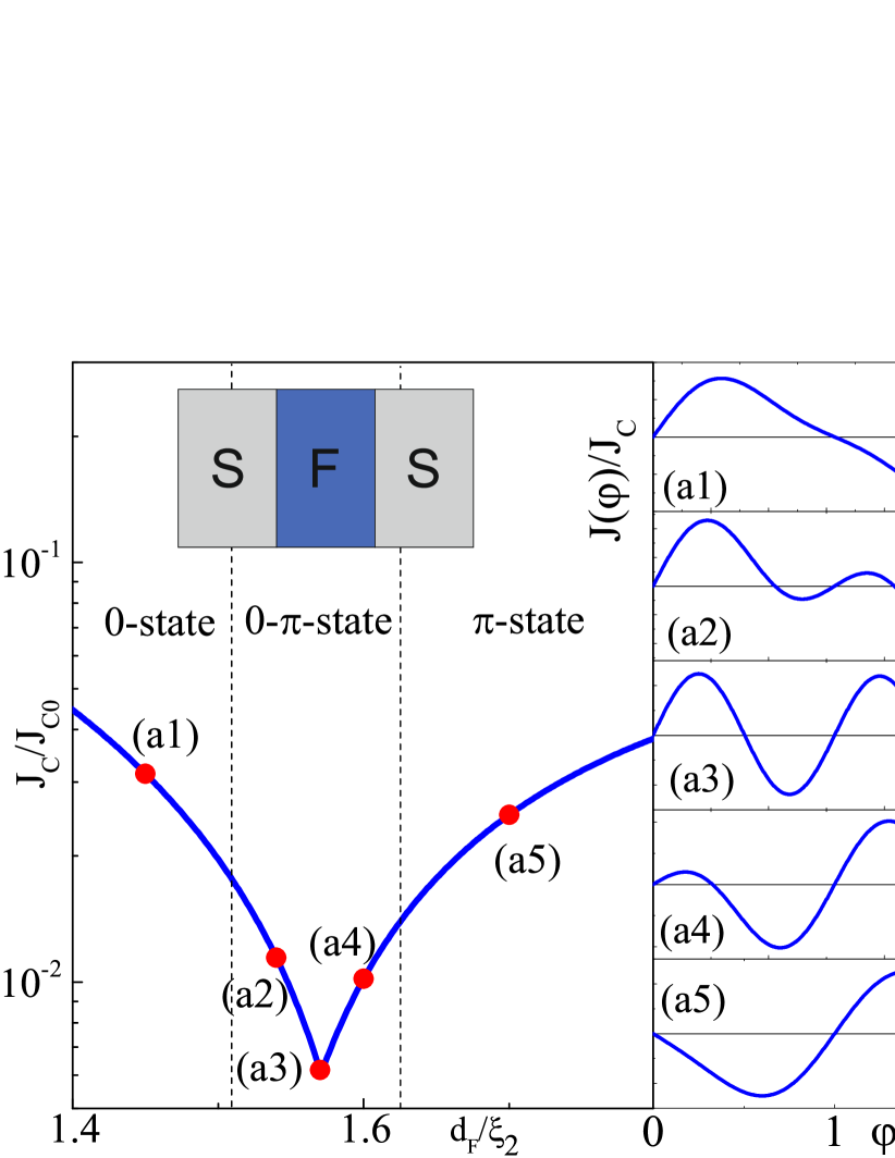
b)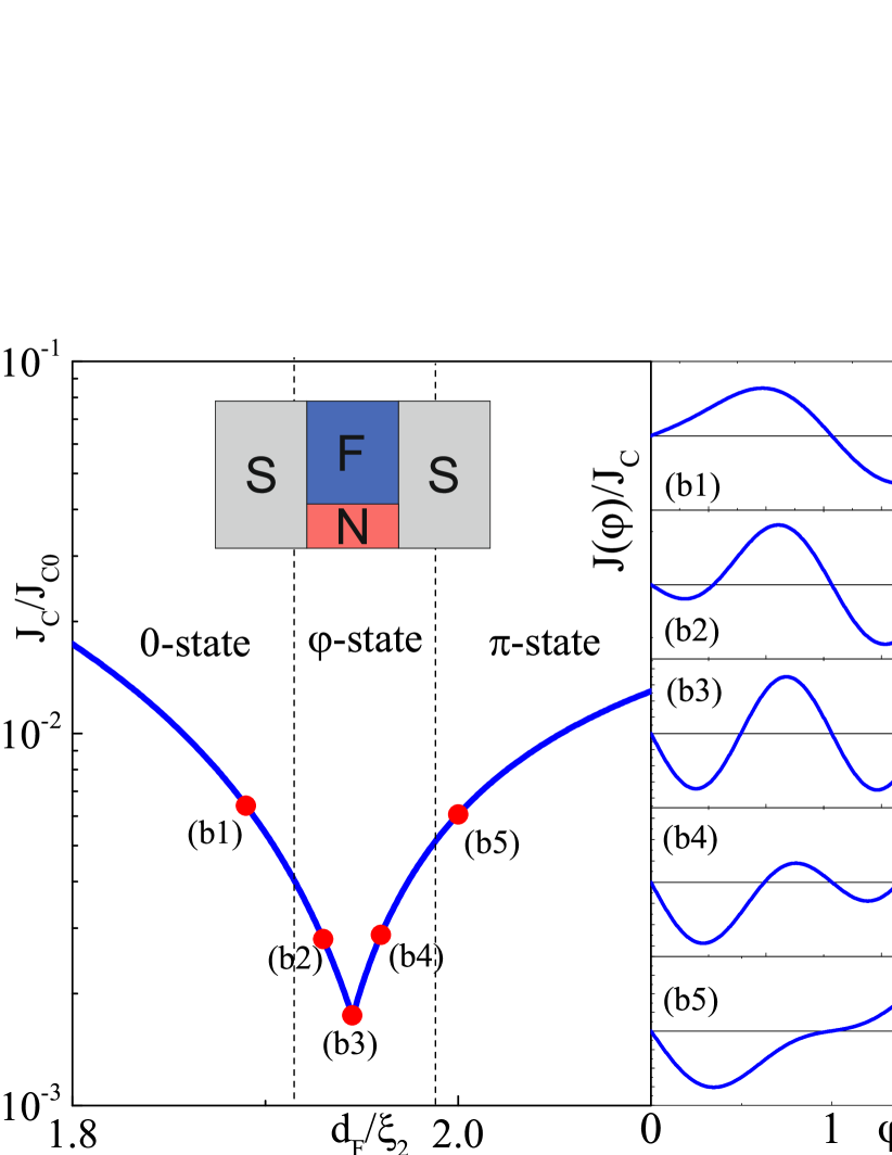
c)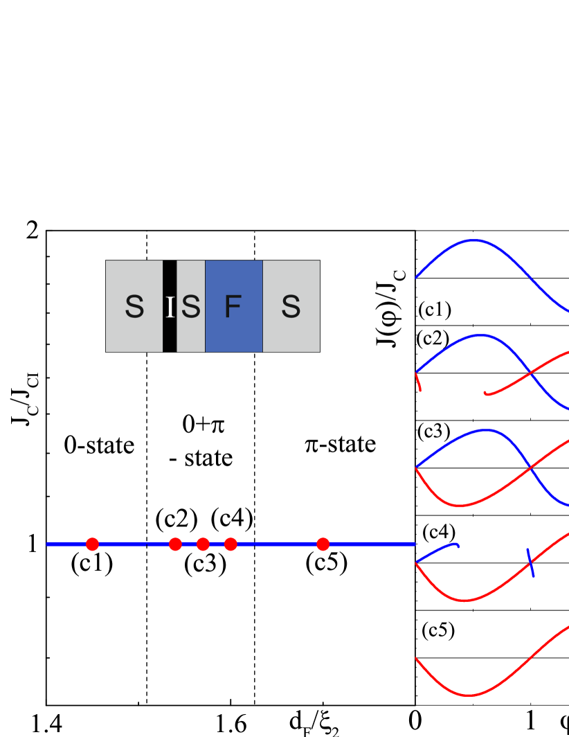
In both transitions presented in Fig.1a,b the curves are V-shaped with a strong suppression of the critical current during the transitions. The metastable states in both structures generally have different barriers, which would be exceeded to switch device into resistive regime. It provides opportunity to read the state, although after that the state will be erased.
Contrary to that, in SIsFS devices SIsFS2013 ; Nevirkovets1 ; Ruppelt ; Nevirkovets2 ; SIsFS2017 it is possible to realize the mode of operation in which magnitude of of SIs part of the structure is smaller than the amplitude of the second harmonic in CPR of its sFS part. In this case (see Fig. 1c) is constant during the transition Ruppelt ; SIsFS2017 , although the current-phase relations undergo significant transformations and become multivalued. For relatively large layer thickness there is the domain of SIsFS junction parameters providing its stay either in - or in -ground state. The critical current is determined by SIs part of the junction and is exactly the same for the both states. In this domain a transition from one ground state to another is not possible by a continuous adiabatic variation of the phase and the states can be used for storage an information since the energy barrier separated them is higher than the energy of tunnel junction, thus protecting the system against accidental switching.
In order to model the SIsFS structure we suppose that the condition of a dirty limit is fulfilled for all metals and that effective electron-phonon coupling constant is zero in F layer. Under the above conditions the problem can be analyzed in the framework of the Usadel equations Usadel with Kupriyanov-Lukichev boundary conditions KL at the interfaces. The boundary-value problem was solved numerically using the algorithm developed in Ref. SIsFS2017 . For simplicity we assume below that the resistivities and coherence lengths of the SIsFS junction materials are the same. Here is a critical temperature and is a diffusion coefficient of superconducting material.
Based on our previous investigations SIsFS2017 ; SIsFS2013 we have fixed the set of SIsFS junction parameters that ensure an occurrence of SIsFS contact in the vicinity of the transition at large s layer thickness : , , exchange energy suppression parameters of SF interface and SIs interface . Here and are the resistance and area of corresponding interface. With this choice of parameters the weakest link of the SIsFS structure is located at the tunnel barrier thus providing the coexistence of the two independent CPR branches (see example in the panel (c3) in Fig. 1c).
We start with calculation of the dependence of magnitude on , shown as a blue line in Fig. 2. It has a common form with a rapid drop of the critical current near the critical thickness . There are two independent processes going in the vicinity of this point. The first one is a shifting of the position and narrowing of the width of the transition during the decrease of the , due to the change of the effecting boundary condtions on F layer Vernik . Inset in the Fig. 2 shows that transformation significantly differs from the process studied in the SInFS junction Pugach1 , since the residual pairing locks the phases of different Matsubara frequencies. This phenomenon leads to collapse of the 0-branch of the CPR at the near the critical point.
The second phenomenon is the deviation of the pair amplitude in the thin s-electrodes for and states due to the different symmetry of the anomalous Green functions predicted and found experimentally in the sFs junctions with thin s-electrodes Samokhvalov1 ; Samokhvalov2 ; Samokhvalov3 . This effect can modify the critical currents of the tunnel SIs junction due to the changing of the s-layer properties in and states.
The relative impact of these processes on the SIsFS structure properties depends on the tunnel suppression parameter . First, we consider the system at , when the collapse of the 0-branch occurs.
a)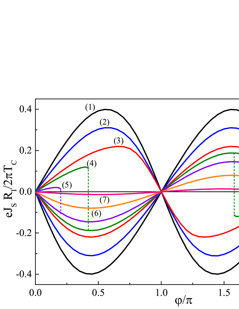
b)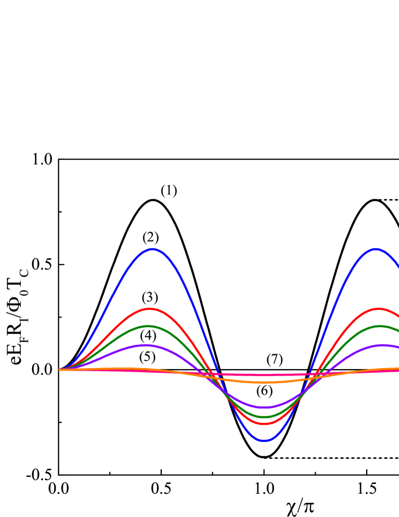
Figure 3a demonstrates the evolution of the shape of dependence with decrease of the s layer thickness. It is seen that the magnitudes of critical current of the both CPR branches are monothonically decreasing, while the shape of the curves transforms in different ways. The CPR of the ground state remains sinusoidal at any during the decrease. The CPR at the some the -branch becomes broken and disappears in the significant interval of phases. At it completely disappears and only the ground state still exists. At the smaller critical current of the -branch is strongly suppressed due to intensive suppression of the superconductivity in the s-layer by inverse proximity effect.
To understand the physics behind the transformations shown above it is convenient to use the so-called lump junction model SIsFS2017 and consider the SIsFS junction as a series connection of SIs and sFS contacts with finite thickness of the s electrode. The self-consistent problem for sFS junction was solved numerically with free boundary condition at the Is interface. The choice of the initial pair potential in iterative self-consistent calculation permits to find the magnitudes of Usadel functions at Is interface for both 0 and -states. Taking into account that the supercurrent flowing across the SIsFS structure is essentially small compare to s and S films depairing current, and that the thicknesses of interest exceed we can neglect a dependence of magnitudes on phase differences and across both sFS and SIs junctions, respectively. Under this assumption the critical current, and energy phase relation, of SIs contact can be calculated using standard well-known expressions
| (1) | |||
| (2) |
where is the resistance of the tunnel barrier and is the magnetic flux quantum.
In the considered approximation the same quantities can be used as boundary conditions of the first kind in calculating CPR and EPR
| (3) |
of sFS contact (see Fig. 3b).
Figure 3b demonstrates that dependence have the double-well form with the two minima at and separated by a potential barrier . The decrease of is accompanied by suppression of the barrier height, At the potential barrier completely disappears and the sFS contact stays only in the ground state. The depth of the potential well for the -state also decreases rapidly with further decrease of
We summarize the dependence of the characteristical energies (dashed black), (dash-dotted green) and versus thickness in Fig. 4. The energy of tunnel junction is calculated in the frame of lumped junction model independently for 0- (solid red) and - (short-dashed blue) states of sFS-electrode. It is seen, that they practically coincide with each other for . The blue dots mark the critical energies of the SIsFS junction shown in the Fig. 3. They correllate well with the results obtained in lumped junction model thus demonstrating the accuracy of our approach.
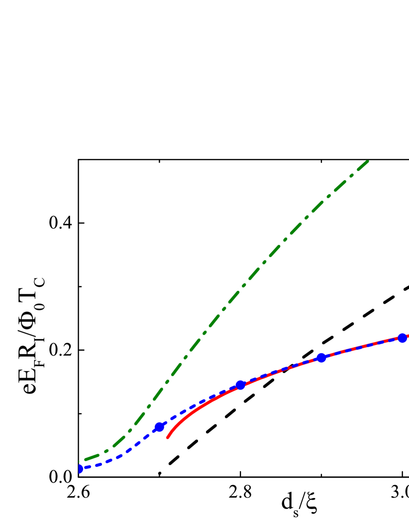
It follows from Fig. 4, that in the wide range of the tunnel energy . These conditions provide existence of two independent continuous branches of CPR in SIsFS junction for the both - and -states as it is seen in Fig. 3a. With the decrease of , the barrier height is suppressed more rapidly than . At the energies and become comparable and adiabatic increase of leads to escape of the system from the metastable to the ground state resulting in discontinues jump in Finally, at the critical thickness the barrier completely vanishes, leading to dissappearence of the 0-branch. At the same time, the barrier for the -state significantly exceeds in the whole considered interval.
In the region near the critical thickness the energies of tunnel SIs junction corresponding to - (red) and - (blue) states deviate. The absolute values of Green function and pair potential on the tunnel SIs interface are different for 0 and states. In contrast to Ref.Samokhvalov1 ; Samokhvalov2 ; Samokhvalov3 , we find that -state has a larger value of and larger critical current.
The difference between and -states provides significant influence on the CPR and critical current of SIsFS structure at the larger values of tunnel layer parameter . Increase of doesn’t modify the barrier height of the SFs-junction, but proportionally decreases the , shifting the cross-point between them to the critical thickness .
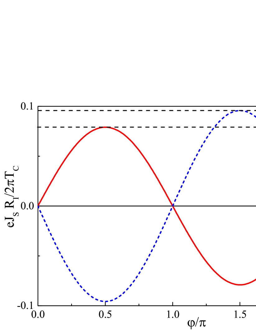
For instance, for the value of suppression parameter direct calculations of SIsFS structure show that the both branches of CPR have sinusoidal shape and are defined for all phases even at (See Fig. 5). It is important to note that for this particular case the critical currents and of - and - CPR branches are different from each other and this difference is of the order .
The ability of the structure to be in one of two states differing in their critical currents can find applications in superconductor logic and memory devices. Information on the state of the SIsFS structure can be obtained by setting a current pulse, with an amplitude, in the range . It is determined by the absence ( state) or by the generation ( state) of the corresponding voltage pulse. Reading the state of the element will be non-destructive, if the incoming energy is insufficient to open the channel of tunneling through the energy barrier separating the and states. The recording is possible with current pulses, which have an amplitude exceeding the critical current of sFS junction and switch the system from 0 to - state and back GoldButterfly .
The drawback of this concept is in strong limitation on thickness of both the superconducting and ferromagnetic layers and the smallness of the critical currents. The thickness of the s layer should be close to its critical value with an accuracy of the order of nm, while the thickness of the ferromagnet should ensure the occurence of that transition. On the other hand, recent experiments Baek2018 ; Frolov2018 have demonstrated the feasibility of this task.
The advantages of the proposed SIsFS element compared to spin-valves Bell ; Qader ; Baek ; Birge2018 or single flux quantum (SFQ) devices Krasnov ; Averin are obvious. The proposed control memory element stores an information only in the phase difference across the junction in the steady state. Thus, it makes use of its own intrinsic properties to store an information, so that there is neither need in remagnetization of the F layers, nor in holding a flux quantum.
In this sense, the bistable SIsFS device may serve as a truly Josephson memory device, which permits the reduction of size of the auxiliary circuits or even provide an alternative to the SFQ concept of superconducting electronics.
Acknowledgments. The authors acknowledge helpful discussion with V.V. Ryazanov and V.V. Bol’ginov. The design of the memory concept was supported by the Russian Science Foundation (12-17-01079) and numerical study of sFS junction was done with support of RFBR (18-32-00672 mol-a).
References
- (1) M. Eschrig, Reports on Progress in Physics, 78, 104501 (2015).
- (2) J. Linder, J. W. A. Robinson, Nature Physics, 11, 307 (2015).
- (3) M. G. Blamire, J. W. A. Robinson, Journ. Phys. Cond. Mat., 26, 453201 (2014).
- (4) J. W. Lu, E. Chen, M. Kabir, V. R. Stan, S. A. Wolf, Int. Materials Reviews 61, 456 (2016).
- (5) O. A. Mukhanov, Digital Processing, Superconductor Digital Electronics. In Applied Superconductivity: Hand-book on Devices and Applications; Seidel, P., Ed., Wiley-VCH Verlag GmbH & Co. KGaA: Weinheim, Germany (2015).
- (6) I. I. Soloviev, N. V. Klenov, S. V. Bakurskiy, M. Yu Kupriyanov, A. L. Gudkov, and A. S. Sidorenko, Beilstein Journal of Nanotechnology, 8, 2689 (2017).
- (7) A. A. Golubov, M. Yu. Kupriyanov, E. Il’ichev, Rev. Mod. Phys. 76, 411 (2004).
- (8) A. I. Buzdin, Rev. Mod. Phys. 77, 935 (2005).
- (9) F. S. Bergeret, A. F. Volkov, K. B. Efetov, Rev. Mod. Phys. 77, 1321 (2005).
- (10) C. Bell, G. Burnell, C. W. Leung, E. J. Tarte, D.-J. Kang and M. G. Blamire, Appl. Phys. Lett., 84, 1153 (2004).
- (11) M. A. E. Qader, R. K. Singh, Sarah N. Galvin, L. Yu, J. M. Rowell, and N. Newman, Appl. Phys. Lett., 104, 022602 (2014).
- (12) B.Baek, W.H.Rippard, S.P.Benz, S.E.Russek, and P.D. Dresselhaus, Nature Communications, 5, 3888 (2014).
- (13) B. M. Niedzielski, T. J. Bertus, J. A. Glick, R. Loloee, W. P. Pratt, Jr., and N. O. Birge Phys. Rev. B 97, 024517 (2018).
- (14) V. V. Bol’ginov, V. S. Stolyarov, D. S. Sobanin, A. L. Karpovich, and V. V. Ryazanov, Pis’ma v ZhETF 95, 408 (2012) [JETP Lett. 95 366 (2012)].
- (15) T. I. Larkin, V. V. Bol’ginov, V. S. Stolyarov, V. V. Ryazanov, I. V. Vernik, S. K. Tolpygo, and O. A. Mukhanov, Appl. Phys. Lett. 100, 222601 (2012).
- (16) I. V. Vernik, V. V. Bol’ginov, S. V. Bakurskiy, A. A. Golubov, M. Yu. Kupriyanov, V. V. Ryazanov and O. A. Mukhanov, IEEE Tran. Appl. Supercond., 23, 1701208 (2013).
- (17) S. V. Bakurskiy, N. V. Klenov, I. I. Soloviev, V. V. Bol’ginov, V. V. Ryazanov, I. I. Vernik, O. A. Mukhanov, M. Yu. Kupriyanov, and A. A. Golubov, Appl. Phys. Lett. 102, 192603 (2013).
- (18) R. Caruso, D. Massarotti, A. Miano, V. V. Bol ginov, A. Ben Hamida, L. N. Karelina, G. Campagnano, I. V. Vernik, F. Tafuri, V. V. Ryazanov, O. A. Mukhanov, and G. P. Pepe, IEEE Trans. Appl. Supercond., 28, 7, 1800606, (2018).
- (19) R. Caruso, D. Massarotti, V. V. Bolginov, A. Ben Hamida, L. N. Karelina, A. Miano, I. V. Vernik, F. Tafuri, V. V. Ryazanov, O. A. Mukhanov, G. P. Pepe, Journ. Appl. Phys., 123, 133901 (2018).
- (20) I. I. Soloviev, N. V. Klenov, S. V. Bakurskiy, V. V. Bol’ginov, V. V. Ryazanov, M. Yu Kupriyanov, and A. A. Golubov, Appl. Phys. Lett., 105, 242601 (2014).
- (21) I. I. Soloviev, N. V. Klenov, S. V. Bakursky, M. Yu Kupriyanov, and A. A. Golubov, JETP Letters, 101, 240 (2015).
- (22) S. V. Bakurskiy, N. V. Klenov, I. I. Soloviev, M. Yu Kupriyanov, and A. A. Golubov, Appl. Phys. Lett., 108, 042602 (2016).
- (23) E. Goldobin, H. Sickinger, M. Weides, N. Ruppelt, H. Kohlstedt, R. Kleiner, D. Koelle, Appl. Phys. Lett. 102 (24), 242602 (2013).
- (24) R. Menditto, H. Sickinger, M. Weides, H. Kohlstedt, M. Zonda, T. Novotny, D. Koelle, R. Kleiner, E. Goldobin, Physical Review B 93 (17), 174506 (2016).
- (25) J. J. A. Baselmans, T. T. Heikkila, B. J. van Wees, and T. M. Klapwijk, Phys. Rev. Lett. 89, 207002 (2002).
- (26) S. M. Frolov, D. J. Van Harlingen, V. A. Oboznov, V. V. Bolginov, and V. V. Ryazanov, Phys. Rev. B 70, 144505 (2004).
- (27) B. Baek, M. Schneider, M. R. Pufall, W. H. Rippard, IEEE Tran. Appl. Supercond., 28, 7, 1800705 (2018).
- (28) M.J.A. Stoutimore, A.N. Rossolenko, V.V. Bolginov, V.A. Oboznov, A.Y. Rusanov, N. Pugach, S.M. Frolov, V.V. Ryazanov, D.J. Van Harlingen, arXiv:1805.12546 (2018).
- (29) L. Trifunovic, Z. Popovic, and Z. Radovic Phys. Rev. B 84, 064511 (2011).
- (30) C. Richard, M. Houzet, J. S. Meyer, Phys. Rev. Lett., 110 (21), 217004 (2013).
- (31) A. Buzdin Phys. Rev. B 72, 100501(R) (2005).
- (32) F. Konschelle, J. Cayssol, A.I. Buzdin, Phys. Rev. B 78, 134505 (2008).
- (33) A. Buzdin and A. E. Koshelev, Phys. Rev. B 67, 220504(R) (2003).
- (34) N. G. Pugach, E. Goldobin, R. Kleiner, D. Koelle, Physical Review B, 81(10), 104513 (2010).
- (35) E. Goldobin, D. Koelle, R. Kleiner, and R.G. Mints, Phys. Rev. Lett, 107, 227001 (2011).
- (36) S. V. Bakurskiy, N. V. Klenov, T. Yu. Karminskaya, M. Yu. Kupriyanov, and A. A. Golubov, Supercond. Sci. Technol. 26, 015005 (2013).
- (37) H. Sickinger, A. Lipman, M. Weides, R. G. Mints, H. Kohlstedt, D. Koelle, R. Kleiner, E. Goldobin, Phys. Rev. Lett. 109, 107002 (2012).
- (38) S. V. Bakurskiy, N. V. Klenov, I. I. Soloviev, M. Yu. Kupriyanov, and A. A. Golubov, Phys. Rev. B 88, 144519 (2013).
- (39) I. P. Nevirkovets, O. Chernyashevskyy, G. V. Prokopenko, O. A. Mukhanov, J. B. Ketterson, IEEE Trans. on Appl. Supercon. 24, 4, (2014).
- (40) N. Ruppelt, H. Sickinger, R. Menditto, E. Goldobin, D. Koelle, R. Kleiner, O. Vavra, H. Kohlstedt, Appl. Phys. Lett., 106, 022602 (2015).
- (41) S. Shafranjuk, I. P. Nevirkovets, O. A. Mukhanov, and J. B. Ketterson, Phys. Rev. Applied 6, 024018, (2016).
- (42) S. V. Bakurskiy, V. I. Filippov, V. I. Ruzhickiy, N. V. Klenov, I. I. Soloviev, M. Yu Kupriyanov, and A. A. Golubov, Phys. Rev. B 95, 094522 (2017).
- (43) K. D. Usadel, Phys. Rev. Lett. 25, 507 (1970).
- (44) M. Yu. Kuprianov and V. F. Lukichev, Zh. Eksp. Teor. Fiz. 94, 139 (1988) [Sov. Phys. JETP 67, 1163 (1988)].
- (45) D. M. Heim, N. G. Pugach, M. Yu. Kupriyanov, E. Goldobin, D. Koelle, R. Kleiner, N. Ruppelt, M. Weides, H. Kohlstedt, New J. Phys. 17 113022 (2015).
- (46) N. Pompeo, K. Torokhtii, C. Cirillo, A. V. Samokhvalov, E. A. Ilyina, C. Attanasio, A. I. Buzdin, and E. Silva Phys. Rev. B 90, 064510 (2014).
- (47) A. V. Samokhvalov and A. I. Buzdin, Phys. Rev. B 92, 054511 (2015).
- (48) S. N. Vdovichev, Yu. N. Nozdrin, E. E. Pestov, P. A. Yunin, A. V. Samokhvalov, JETP Lett. 104, 329 (2016).
- (49) T. Golod, A. Iovan, V. M. Krasnov, Nature communications 6, 8628 (2015).
- (50) A. Murphy, D. Averin, A. Bezryadin, New J. Phys. 19 (6), 063015 (2017).