Present address: ]Microsoft Station Q and QuTech, Delft University of Technology, 2628 CJ, Delft, Netherlands
Kondo Correlation Induced Low-Field Magnetoresistance Anomalies in InSb Nanowire Josephson Quantum Dot Devices
Abstract
We report the observation of sharp suppression of superconductivity-induced zero-bias conductance peaks at low magnetic fields in InSb nanowire Josephson quantum dot devices. With multiple gates, the quantum dot devices can be tuned to the Kondo-superconductivity interplaying regime, in which Kondo-enhanced superconductivity manifests as a zero-bias conductance peak. In weak magnetic fields, the zero-bias conductance peak is found to exhibit an unusual negative magnetoresistance when the Kondo temperature is comparable to the superconductor gap. The observation could not be explained by magnetic field induced “0-” phase transition, topological phase transition, or other known mechanisms, but may arise from correlation induced interference when Cooper pairs cotunnel through the quantum dots.
External magnetic field in general breaks Cooper pairs by orbital effect Gennes1964 and/or Zeeman effect Gennes1989 and, thereby, suppresses superconductivity. Nevertheless, the magnetic field induced/enhanced superconductivity was proposed theoretically Jaccarino1962 ; Maekawa1978 and observed experimentally in rare-earth compounds and organic conductors Meul1984 ; Uji2001 , where exchange interaction induced by internal magnetic moments can be compensated by externally applied magnetic field (the Jaccarino-Peter effect). Soon after, anomalous field enhanced/induced superconductivity was also discovered in non-Jaccarino-Peter materials, mostly in superconductor thin films Kogan1987 ; Seguchi1993 ; Parendo2004 ; Gardner2011 and superconductor nanowires Xiong1997 ; Bonetto1998 ; Rogachev2006 ; Tian2005 ; Chen2009 ; Chen2011 . Several explanations have been proposed for the counterintuitive field-enhanced superconductivity, but a thorough understanding has not yet been achieved. One plausible proposal suggests that the spin-flipping (Kondo correlation) induced pair-breaking effect could play a key role in superconductors that are doped (intentionally or unintentionally) with magnetic impurities Abrikosov1969 ; Maki1969 . This pair-breaking effect can be suppressed by either raising temperature beyond the Kondo temperature Maple1972 or polarizing paramagnetic impurities by a magnetic field Maki1969 ; Maple1972 ; Wei2006 ; Yuval2012 . However, in the systems mentioned above, the concentration and distribution of the magnetic impurities are difficult to control and, therefore, the magnetic-impurity-related enhancement/reentrance of the superconductivity in magnetic fields is difficult to validate directly.
The rich correlation physics of the magnetic impurity in a superconductor could also be studied by employing a superconductor-quantum dot-superconductor device (i.e., a Josephson quantum dot junction device). In such a device, the quantum dot can be tuned to a spinful ground state [Fig. 1(a)] and, with an unpaired spin inside, is an analog of a single magnetic impurity, yet being highly manipulable. Tuning the device to an odd-number electron occupation in the dot with a sufficiently strong dot-lead coupling, a constructive coherent spin-flipping process occurs and results in an increased conductance, i.e., the Kondo resonance (see the review paper Ref. Kouwenhoven2001 and references therein). In a Josephson quantum dot device, the dot-lead Kondo correlation competes with the condensation energy of the superconductor leads Franke2011 . However, the tunneling transparency enhancement gained from the Kondo correlation could increase the probability of Cooper pair cotunneling and induce a zero-bias conductance peak Rasmussen2007 . By measuring the magnetoresistance of the Josephson quantum dot system with a tunable Kondo temperature, we can investigate the novel physics arising from the interplays between the superconductivity and the Kondo correlations.
It has been demonstrated that in a Josephson quantum dot device with the quantum dot in close proximity to a pair of superconductor leads, dissipationless supercurrent can flow through the entire junction when the dot is in the open or resonant tunneling regime Doh2005 ; Nilsson2012 ; Jarillo2006 . Supercurrent will be greatly suppressed in the deep Coulomb blockade regime of the dot, where Cooper pair transport has to take the form of high order cotunneling processes mediated by several virtual sequential quasiparticle tunneling events. Normally, the cotunneling processes will pick up an additional 0 or phase shift, depending on whether the ground state of the quantum dot is a spin singlet or a spin doublet vandam2006 ; Jorgensen2007 ; Li2017 . In general, at zero magnetic field, an quantum dot with an even-number occupation corresponds to a spin singlet state, while an quantum dot with an odd-number occupation corresponds to a spin doublet state. However, in the presence of a strong dot-lead Kondo correlation, local pairing can prevail local magnetism and the dot can maintains at a spin singlet state even at an odd-number occupation Maurand2012 ; Lee2014 ; Chang2013 . In this case, application of an external magnetic field can induce a singlet-to-doublet phase transition (also called “0-” phase transition) and leads to the emergence of a zero-energy Andreev bound state (ABS) Lee2014 with a suppression of the critical current at the transition point Jorgensen2007 . Moreover, a magnetic field can change the relative strengths of the Kondo correlations and the superconducting condensation energy and can thus cause reentrance of the Kondo anomaly Lee2012 .
In this Letter, we report on transport spectroscopy measurements of Josephson quantum dot devices made from InSb nanowires. The Josephson quantum dot devices can be tuned into the Kondo regime with different strengths of Kondo correlations. In the strong Kondo regime, an enhanced superconductivity manifested by a zero-bias conductance peak is observed. In the regime with moderate Kondo correlations, an anomalous suppression of the zero-bias conductance at zero and small magnetic fields is observed. In contrast, this low-field suppression of the zero-bias conductance is absent in the open-dot regime. With careful characterization, we find that the anomalous low-field suppression of the Josephson superconductivity can not be interpreted by a known mechanism, but it is consistent with an interference-based process where Cooper pairs tunnel through the quantum dots via two Kondo correlation induced many-body states.
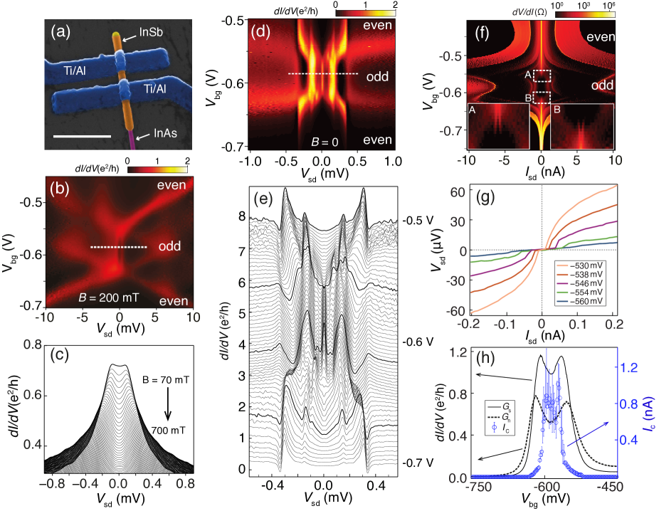
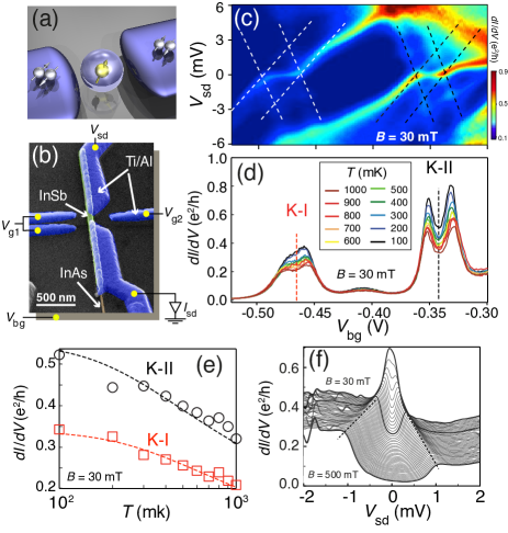
Device details and experiment setup. —Three devices are studied here, denoted as Device 1, Device 2 and Device 3 (Device 3 is only described in the Supplemental Materials), and each constitutes an InSb nanowire quantum dot and two Al superconductor leads [as shown in Fig. 1(b)]). For device fabrication details, please see Ref. Nilsson2012 and references therein. In such a device, a quantum dot is naturally formed in the nanowire segment between the two leads Nillson2009 . The quantum state of the dot and the dot-lead coupling can be tuned by back gate voltage and side gate voltages and . A source-drain bias voltage, , is antisymmetrically applied, i.e., with and applied to the source and drain contacts, using a home-made DC voltage source with a 2 V resolution. Current is measured through a home-made amplifier, and it is then converted to differential conductance numerically. Gate voltages are applied from commercial DC voltage sources. Unless the temperature is specified, all measurements are performed in a 3He/4He dilution refrigerator (wet) at the base cryogenic temperature of 25 mK. All applied magnetic fields are perpendicular to the device substrates. To avoid heating effect from magnetic field sweep, the climbing rate of the magnet is limited below 10 mT/min. Crossing zero-field heating effect is specially checked and avoided.
Low temperature transport measurements. —With application of a 30 mT magnetic field, the superconductivity of the Al leads is suppressed and the device is in the normal state. As shown in Fig. 1(c), the differential conductance, , of Device 1 measured as a function of and displays typical life-time broadened Coulomb blockade diamond structures with a charging energy of meV. Two horizontal high conductance anomalies at zero-bias voltage emerge inside the diamonds at V to V and V to V. Figure 1(d) shows linear response conductance measurements in the same back gate voltage range as in Fig. 1(c) at different temperatures. The conductances of the two zero-bias anomalies—now marked as “K-I” and “K-II”—drop as the temperature increases. See also Fig. 1(e) for the conductances as a function of temperature extracted at the “K-I” and “K-II” valleys from Fig. 1(d). From Figs. 1(c) to 1(e), we can attribute the zero-bias anomalies to the Kondo effect Kouwenhoven2001 . According to the temperature dependence measurements and using the following relation, , where and Gordon1998 , we can estimate the Kondo temperature and obtain K at the K-I Kondo ridge and K at the K-II Kondo ridge. We have also extracted from the full width at half maximum (FWHM) of each corresponding Kondo peak Buitelaar2002 and found K at the K-I ridge and K at the K-II ridge, which are close to the values deduced from the temperature dependence measurements. Figure 1(f) shows the magnetic field dependent measurements at mV, where the K-I Kondo conductance ridge is seen to split due to the Zeeman effect. An effective -factor can be extracted by a linear fit to the splitting, yielding .
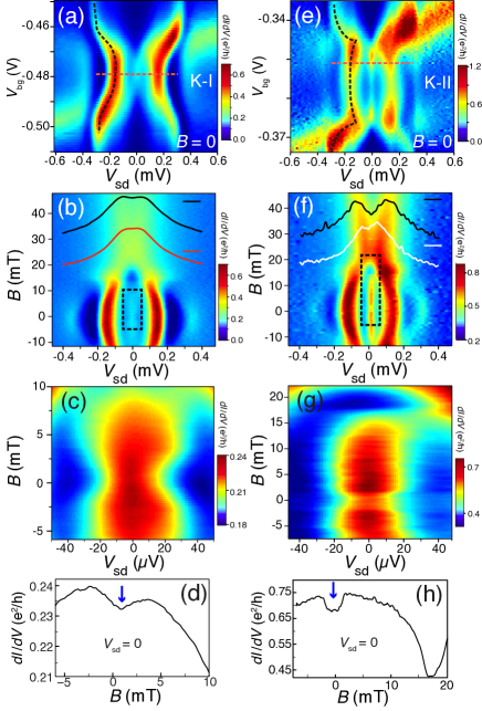
The conductance spectrum of the device can be greatly modulated when the leads are at the superconducting state. Figure 2(a) shows the low-energy conductance spectrum of Device 1 measured at zero magnetic field and in the back gate voltage region where the device would display the K-I Kondo ridge at the normal state. Here, it is seen that two high conductance stripes, bounded by , emerge as sub-gap structures in this back gate voltage region. Figure 2(b) shows the magnetic field dependent measurements at a fixed back gate voltage denoted by the red dashed line in Fig. 2(a). It is seen that with increasing magnetic field, the two conductance peaks move towards lower energies. When the magnetic field goes above mT, the two peaks vanish and the device shows a recovered Kondo resonant peak [see, e.g., the red and black line cuts in Fig. 2(b)]. These finite-bias transport features at zero and low fields, together with more sub-gap structures that will be shown in the following figures, could be attributed to multiple Andreev reflections (MAR), ABS, and/or their interplays with Kondo resonances. Already covered by many landmark papers Buitelaar2003 ; Jespersen2007 ; Eichler2007 ; Kim2013 , these sub-gap structures found in the this work will not be further discussed in details.
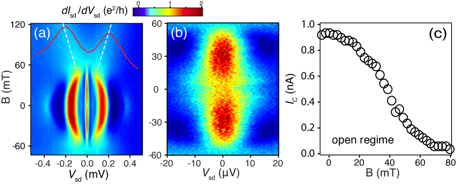
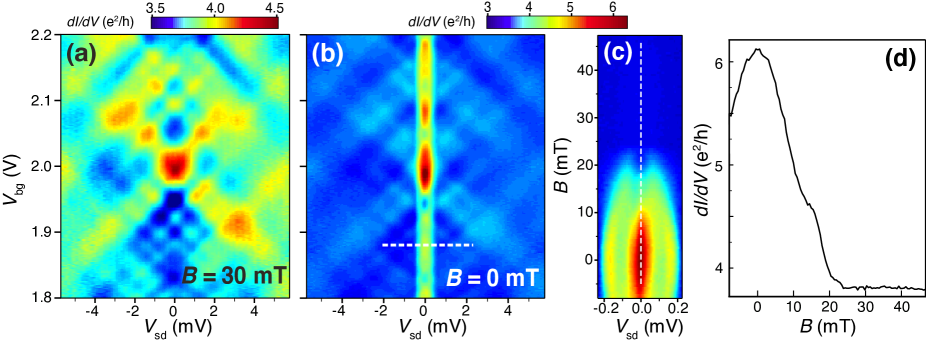
There is a weak zero-bias conductance peak around mV in Fig. 2(a). This zero-bias peak extends from mT to mT and shows surprisingly a conductance dip, i.e., negative magnetoresistance (NMR) characteristics, in the range of to mT [see the close-up view in Fig. 2(c) and the line-cut plot along -axis at in Fig. 2(d)]. A similar zero-bias peak is found in the K-II gate voltage region [Fig. 2(e)]. In contrast to the smooth magnetoresistance trace seen in the K-I gate voltage region, the zero-bias peak in the K-II region displays a more pronounced NMR, see the steeper conductance dip in magnetic fields below mT in Figs. 2(f) to 2(h). The curvatures of the finite-bias peaks (guided by the black dashed lines) in Figs. 2(a) and 2(e) indicate that the Josephson quantum dot device forms a “0”-junction in the K-I region, but a “”-junction in the K-II region Kim2013 .
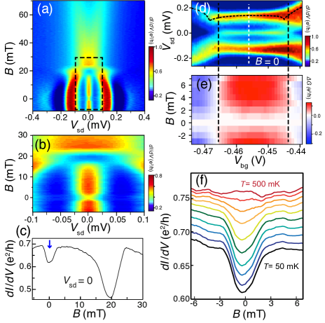
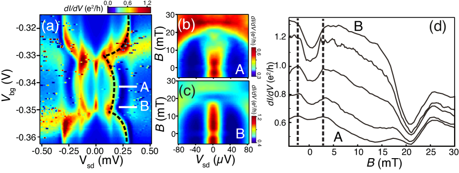
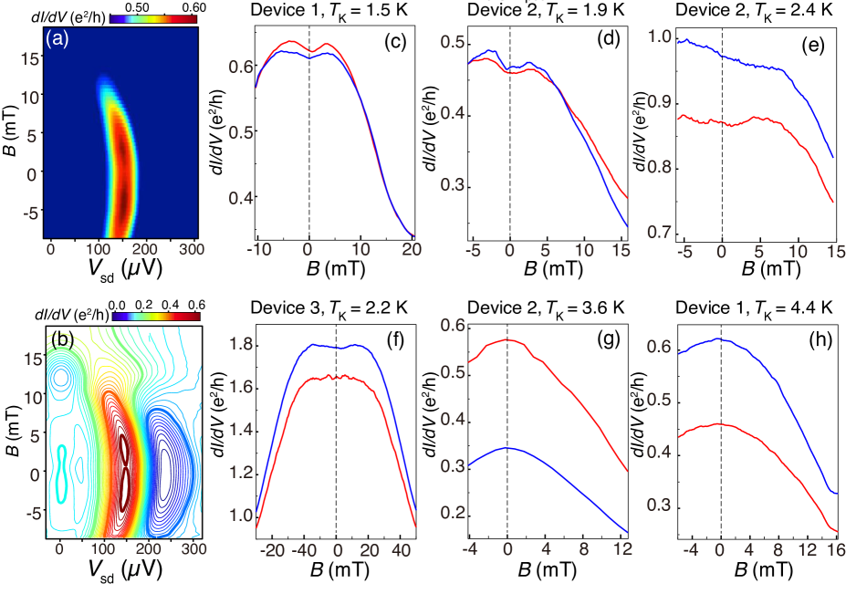
We have also measured Device 2, which is lithographically identical to Device 1. By using both the back gate and the side gates, we can also tune Device 2 to an odd-number electron occupied Coulomb blockade region with a zero-bias peak, as shown in Figs. 3(a)-3(c). The zero-bias conductance of Device 2 again shows a strong NMR at low fields with a steep conductance valley in the range of mT to 3 mT. From the profile of the finite-bias conductance peaks in Fig. 3(d), the quantum dot is seen to be in the “”-junction regime. To see how the NMR varies with gate voltage, we define zero-bias magnetoconductance as the difference between the conductance values measured at finite field and at zero field, and extracted as a function of and [Fig. 3(e)]. It is evident that the NMR is present in the entire zero-bias peak region shown in Fig. 3(d), with a similar conductance valley width (i.e., all appear roughly at magnetic fields of -3 mT to 3 mT). We have also performed temperature dependence measurements of the zero-bias peak at small magnetic fields [Fig. 3(f)]. The NMR valley is seen to be gradually smeared out and vanishes at temperature around mK, well below the critical temperature of the Al leads ( K).
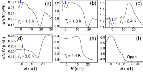
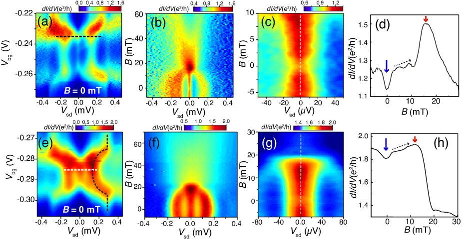
Using back gate and side gates, Device 1 and Device 2 can be tuned to the Kondo resonances with various [Fig. 4]. Surprisingly, all of the zero-bias peaks are associated with a NMR in the range of mT (with some extending to 4 mT). However, the NMR valley is getting much weaker at the zero-bias peaks with a higher [Figs. 4(d) and 4(e)]. In addition, it is seen that in the more positively gate voltage region, where the Coulomb blockade feature is absent and the devices are at the open-dot regime, no NMR characteristics could be observed [Fig. 4(f), see more details in the Supplemental Materials].
We have also fabricated and measured Device 3, which is designed in a different geometry. A zero-bias peak with a NMR is also observed below mT in the device. Note that the critical magnetic field, , is higher than 60 mT in this device. Again, the NMR disappears in the open regime for Device 3. See the Supplemental Materials for further detail. In fact, in all of the InSb nanowire based Josephson devices, which have been characterized, in the open regimes Nilsson2012 ; Deng2012 ; Zuo2017 , the low field NMR is absent. Note that the device in Ref. Nilsson2012 was made from the same materials, fabricated in the same method and measured in the same setup as the devices studied here.
Discussion about the physical origin of the observed NMR. —In this work, the observed zero-bias peaks can be attributed to Kondo-enhanced superconductivity Rasmussen2007 ; Kim2013 . For the NMRs associated with these zero-bias peaks, there are several possible mechanisms which could be ascribed to.
One might consider that the magnetic field could lead to an increase in the ratio and therefore induce a recovered Kondo density of states Lee2012 . However, the NMR only occurs below mT, where has not yet been effectively increased [ at B=3 mT, where is zero-field superconducting gap]. Actually, as shown in the Supplemental Materials, we do observe the coexistence of a recovered Kondo density of states and a weak field NMR valley. However, the recovered Kondo density of states appears at a significantly larger field and the associated conductance has a different magnetic-field dependent line profile (see the Supplementary Materials).
The appearance of the NMRs at very small magnetic fields and their strong relation to the Kondo effect can also explain why field-induced emergent zero-energy ABSs or Majorana bound states Lee2014 ; Chang2013 ; Mourik2012 ; Deng2012 ; Deng2016 are not consistent with the results observed here either. Without considering field screening, a 3 mT magnetic field can only induce a Zeeman energy eV ( is the Bohr magneton) in the InSb nanowire Nillson2009 , which is unlikely sufficient to drive the hybrid structures to the topological regime. We are aware of that Ref. Tiira2017 reported a colossal enhancement of supercurrent that is induced by a weak magnetic field in InAs nanowire based Josephson junctions, which could be related to a topological phase transition induced enhancement in the critical current San-Jose2014 . However, again, the NMR valleys observed in this work appear only when the Kondo correlation is present and thus can not be attributed to such a topological phase transition.
Phase conjugation from weak antilocalization Pikulin2012 can be also ruled out, because a magnetic field of 3 mT only gives an encircled phase, , where is the area that is normal to the magnetic field and is the magnetic flux quantum, according to the geometrical structures of Devices 1 and 2.
The seeming independence and electrode-geometry dependence of the NMR width indicate that the NMRs could be attributed to quasiparticle dynamics of the superconductor leads Chen2014 , such as vortex-induced quasiparticle trapping Taupin2016 or quasiparticle stabilization/cooling Chen2009 ; Chen2011 ; Vodolazov2012 . But it is still not consistent with the fact that the NMRs are only present in the Kondo regime and absent in the open regime.
Another possible explanation for the anomalous NMRs is the magnetic field induced quantum phase transition (QPT). In this case, the Josephson quantum dot is initially at “0-” crossing point at zero field, where the Josephson supercurrent is suppressed. The application of a magnetic field can drive the device away from the crossing point and leads to an increase of (reversal) Josephson current vandam2006 . However, the observed NMRs appear not only at a few points, but also in the entire odd-number electron occupied Coulomb blockade regions in the presence of the Kondo correlations [Fig. 3(e) and the Supplemental Materials]. Thus, the QPT is less likely to be the interpretation for the observed anomalous NMRs in this work.
Finally, inspired by Ref. Nilsson2010 where destructive interference was observed at correlated, spinful level degeneracy points of a quantum dot, the observed NMRs could be attributed to destructive interference of Cooper pairs that pass through the quantum dot via two many-body paths created by the Kondo correlation. As we mentioned above, in the Josephson quantum dot with an unpaired spin, the two electrons of a Cooper pair have to successively tunneling through the dot. However, with a moderate Kondo interaction, the correlated and spins in the dot provides two naturally cotunneling paths with a phase difference of for Cooper pairs, leading to a destructive interference in Cooper pair tunneling through the quantum dot. For a quantum dot with a large g-factor, application of a weak magnetic field can remove the degeneracy of the two spin states and thus destructive interference in Cooper pair cotunneling. We emphasize that the NMRs are observed at the moderate Kondo correlation regime. If the Kondo correlation is too strong, the odd-number electron occupied quantum dot is essentially in the spin singlet state, where Cooper pair directly tunneling is allowed and the above destructive interfering process is suppressed. As a result, the observed NMRs at high- Kondo ridges become much weaker (see Fig. 4). Note that this seemingly appealing explanation needs support from more sophisticated modeling and numerical calculations. Thus, we would like to keep the discussion open at the present stage and call for theoretical studies for the systems.
Conclusion. —We have fabricated and measured three InSb nanowire Josephson quantum dot devices and observed suppression of zero-bias conductance at zero and low magnetic fields in the devices in the presence of the Kondo correlations. This anomalous NMR favors the regime where the Kondo temperature is in the order of the superconducting gap and could likely arise from destructive interference when Cooper pairs cotunnel through the quantum dot via two correlation induced, inseparable many-body states. Though it is still unclear which mechanism should be attributed to, this experiment indicates that the coherent spin-flipping process can play an important role in magnetic impurity-superconductor coupled systems. It also provides a platform for exploring unveiled novel physics in disordered superconductors and Josephson networks/arrays.
We thank M. Leijnse, J Paaske and R Aguado for helpful discussion. This work was financially supported by the Swedish Research Council (VR), the Ministry of Science and Technology of China (MOST) through the National Key Research and Development Program of China (No. 2016YFA0300601 and 2017YFA0303304), and the National Natural Science Foundation of China (Nos. 11874071, 91221202 and 91421303).
References
- (1) P. D. Gennes, and M. Tinkham, Magnetic behavior of very small superconducting particles (Universite de Paris, Orsay, France, 1964), Vol. 1.
- (2) P. D. Gennes, Superconductivity of metals and alloys. (New York: Addison-Wesley, 1989).
- (3) V. Jaccarino and M. Peter, Phys. Rev. Lett. 9, 290 (1962).
- (4) S. Maekawa and M. Tachiki, Phys. Rev. B 18, 4688 (1978).
- (5) H. W. Meul, C. Rossel, M. Decroux, Ø. Fischer, G. Remenyi, and A. Briggs, Phys. Rev. Lett. 53, 497 (1984).
- (6) S. Uji, H. Shinagawa, T. Terashima, T. Yakabe, Y. Terai, M. Tokumoto, A. Kobayashi, H. Tanaka, and H. Kobayashi, Nature 410, 908 (2001).
- (7) V. G. Kogan and Naka, Phys. Rev. B 35, 1700 (1987).
- (8) Y. Seguchi, T. Tsuboi, and T. Suzuki, J. Phys. Soc. Japan 62, 2564 (1993).
- (9) K. A. Parendo, L. M. Hernandez, A. Bhattacharya, and A. M. Goldman, Phys. Rev. B 70, 212510 (2004).
- (10) H. J. Gardner, A. Kumar, L. Yu, P. Xiong, M. P. Warusawithana, L. Wang, O. Vafek, and D. G. Schlom, Nat. Phys. 7, 895 (2011).
- (11) P. Xiong, A. V. Herzog, and R. C. Dynes, Phys. Rev. Lett. 78, 927 (1997).
- (12) C. Bonetto, N. E. Israeloff, N. Pokrovskiy, and R. Bojko, Phys. Rev. B 58, 128 (1998).
- (13) A. Rogachev, T.-C. Wei, D. Pekker, A. Bollinger, P. Goldbart, and A. Bezryadin, Phys. Rev. Lett. 97, 137001 (2006).
- (14) M. Tian, N. Kumar, S. Xu, J. Wang, J. Kurtz, and M. Chan, Phys. Rev. Lett. 95, 4 (2005).
- (15) Y. Chen, S. D. Snyder, and A. M. Goldman, Phys. Rev. Lett. 103, 127002 (2009).
- (16) Y. Chen, Y.-H. Lin, S. D. Snyder, and A. M. Goldman, Phys. Rev. B 83, 054505 (2011).
- (17) Abrikosov, Sov. Phys. Uspekhi 12, 168 (1969).
- (18) K. Maki, Superconductivity, (Marcel Dekker, New York, 1969).
- (19) M. B. Maple, W. A. Fertig, A. C. Mota, L. E. DeLong, D. Wohlleben, R. Fitzgerald, Solid State Communications 11, 829-834(1972).
- (20) T.-C. Wei, D. Pekker, A. Rogachev, A. Bezryadin, and P. M. Goldbart, Europhys. Lett. 75, 943 (2006).
- (21) Y. B. Simons, O. Entin-Wohlman, Y. Oreg, and Y. Imry, Phys. Rev. B 86, 64509 (2012).
- (22) L. Kouwenhoven and L. Glazman, Phys. World 14, 33 (2001).
- (23) K. J. Franke, G. Schulze, and J. I. Pascual, Science 332, 940 (2011).
- (24) K. Grove-Rasmussen, H. I. Jørgensen, and P. E. Lindelof, New J. Phys. 9, 124 (2007).
- (25) Y.-J. Doh, J. A. van Dam, A. L. Roest, E. P. A. M. Bakkers, L. P. Kouwenhoven, and Francesc, Science 80, 272 (2005).
- (26) H. A. Nilsson, P. Samuelsson, P. Caroff, and H. Q. Xu, Nano Lett. 12, 228 (2012).
- (27) P. Jarillo-Herrero, J. A. Van Dam, and L. P. Kouwenhoven, Nature 439, 953-956 (2006).
- (28) J. A. van Dam, Y. V Nazarov, E. P. A. M. Bakkers, S. De Franceschi, and L. P. Kouwenhoven, Nature 442, 667 (2006).
- (29) H. I. Jørgensen, T. Novotnỳ, K. Grove-Rasmussen, K. Flensberg, and P. E. Lindelof, Nano Lett. 7, 2441 (2007).
- (30) S. Li, N. Kang, P. Caroff, and H. Q. Xu, Phys. Rev. B 95, 014515 (2017).
- (31) R. Maurand, T. Meng, E. Bonet, S. Florens, L. Marty, and W. Wernsdorfer, Phys. Rev. X 2, 011009 (2012).
- (32) E. J. H. Lee, X. Jiang, M. Houzet, R. Aguado, C. M. Lieber, and S. De Franceschi, Nat. Nanotechnol. 9, 79 (2014).
- (33) W. Chang, V. E. Manucharyan, T. S. Jespersen, J. Nygård, and C. M. Marcus, Phys. Rev. Lett. 110, 217005 (2013).
- (34) E. J. H. Lee, X. Jiang, R. Aguado, G. Katsaros, C. M. Lieber, and S. De Franceschi, Phys. Rev. Lett. 109, 186802 (2012).
- (35) P. Caroff, J. B. Wagner, K. A. Dick, H. A. Nilsson, M. Jeppsson, K. Deppert, L. Samuelson, L. R. Wallenberg, and L. E. Wernersson, Small 4, 878 (2008).
- (36) H. A. Nilsson, P. Caroff, C. Thelander, M. Larsson, J. B. Wagner, L.-E. Wernersson, L. Samuelson, and H. Q. Xu, Nano Letters 9, 3151-3156 (2009).
- (37) D. Goldhaber-Gordon, J. Göres, M. A. Kastner, H. Shtrikman, D. Mahalu, and U. Meirav, Phys. Rev. Lett. 81, 5225 (1998).
- (38) M. R. Buitelaar, T. Nussbaumer, and C. Schönenberger, Phys. Rev. Lett. 89, 256801 (2002).
- (39) M. R. Buitelaar, W. Belzig, T. Nussbaumer, B. Babić, C. Bruder, and C. Schönenberger, Phys. Rev. Lett. 91, 057005 (2003).
- (40) T. Sand-Jespersen, J. Paaske, B. M. Andersen, K. Grove-Rasmussen, H. I. Jørgensen, M. Aagesen, C. B. Sørensen, P. E. Lindelof, K. Flensberg, and J. Nygård, Phys. Rev. Lett. 99, 126603 (2007).
- (41) A. Eichler, M. Weiss, S. Oberholzer, C. Schönenberger, A. Levy Yeyati, J. C. Cuevas, and A. Martín-Rodero, Phys. Rev. Lett. 99, 126602 (2007).
- (42) B. K. Kim, Y. H. Ahn, J. J. Kim, M. S. Choi, M. H. Bae, K. Kang, J. S. Lim, R. López, and N. Kim, Phys. Rev. Lett. 110, 076803 (2013).
- (43) M. T. Deng, C. L. Yu, G. Y. Huang, M. Larsson, P. Caroff, and H. Q. Xu, Nano Lett. 12, 6414 (2012).
- (44) K. Zuo, V. Mourik, D. B. Szombati, B. Nijholt, D. J. Van Woerkom, A. Geresdi, J. Chen, V. P. Ostroukh, A. R. Akhmerov, S. R. Plissard, D. Car, E. P. A. M. Bakkers, D. I. Pikulin, L. P. Kouwenhoven, and S. M. Frolov, Phys. Rev. Lett. 119, 187704 (2017).
- (45) V. Mourik, K. Zuo, S. M. Frolov, S. R. Plissard, E. P. a. M. Bakkers, and L. P. Kouwenhoven, Science 336, 1003 (2012).
- (46) M. T. Deng, S. Vaitiekėnas, E. B. Hansen, J. Danon, M. Leijnse, K. Flensberg, J. Nygård, P. Krogstrup, and C. M. Marcus, Science 354, 1557 (2016).
- (47) J. Tiira, E. Strambini, M. Amado, S. Roddaro, P. San-Jose, R. Aguado, F. S. Bergeret, D. Ercolani, L. Sorba, and F. Giazotto, Nat. Commun. 8, 14984 (2017).
- (48) P. San-Jose, E. Prada, and R. Aguado, Phys. Rev. Lett. 112, 137001 (2014).
- (49) D. I. Pikulin, J. P. Dahlhaus, M. Wimmer, H. Schomerus, and C. W. J. Beenakker, New J. Phys. 14, 125011 (2012).
- (50) Y. Chen, Y. H. Lin, S. D. Snyder, A. M. Goldman, and A. Kamenev, Nat. Phys. 10, 567 (2014).
- (51) M. Taupin, I. M. Khaymovich, M. Meschke, A. S. Mel’nikov, and J. P. Pekola, Nat. Commun. 7, 10977 (2016).
- (52) D. Y. Vodolazov and F. M. Peeters, Phys. Rev. B 85, 1 (2012).
- (53) H. A. Nilsson, O. Karlström, M. Larsson, P. Caroff, J. N. Pedersen, L. Samuelson, A. Wacker, L. E. Wernersson, and H. Q. Xu, Phys. Rev. Lett. 104, 186804 (2010).
I Supplemental Materials for:
Kondo Correlation Induced Low-Field Magnetoresistance Anomalies in InSb Nanowire Josephson Quantum Dot Devices
The supplemental materials include figures showing measurement results for Device 3 and figures showing supporting datasets for Device 1 and Device 2. Figure descriptions and associated discussions are all presented in the captions.
-
•
Figure 1: Device 3 and its characterization measurements
-
•
Figure 2: Magnetic field dependent measurements of the conductance spectra and the supercurrent in Device 3.
-
•
Figure 3: Observation of the low field NMR in Device 2 in a “”-junction.
-
•
Figure 4: Observation of the coexistence of the anomalous NMR and field-induced recovered Kondo Peak in Devices 1 and 2 close to Coulomb resonances.
-
•
Figure 5: Measurements of the conductance spectra for Device 2 in the open regime.
-
•
Figure 6: Observation of weak NMR features at the finite-bias conductance peaks in all the three studied devices.