Charge-based Model for Ultra-Thin Junctionless DG FETs, Including Quantum Confinement
Abstract
This paper presents a generalization of the charge-based model for ultra-thin junctionless double-gate FETs [1, 2] by including quantum electron density. The analytical derivation relies on a first order correction to the infinite quantum well. When restricting the analysis to the first and second quantized states, the free carrier charge distribution and the current in an ultra-thin body junctionless double gate FETs is in agreement with numerical TCAD simulations in all the regions of operation, i.e. from deep depletion to accumulation and from linear to saturation.
Index Terms:
Junctionless FETs, double-gate FETs, nanowire FETs, quantum well, UTBSOI.I Introduction
Junctionless double-gate and nanowires field-effect transistors are among viable candidates for the next generation of digital and analog applications [3, 4, 5]. In junctionless double-gate FET (JLDG), the channel is uniformly doped from the source to the drain and is controlled by two gates [3, 6]. These devices have no source-drain pn junction, a feature that relaxes some critical processing steps, an advantage over the conventional MOSFETs [7].
A generic charge-based model was proposed for symmetric double-gate structures [1, 8, 2]. In that derivation, non-degenerate Boltzmann statistic and 3D density of states were used to obtain the surface electric-field and the surface potential in the channel. The model predicts accurately DC and AC electrical behaviors from depletion to accumulation [1, 2, 9, 10], but neglects channel quantization, which is not a valid assumption for silicon layers below . Similarly, at high gate overdrive voltages, the Boltzmann statistics combined with the 2D density of states tends to overestimate the free carrier densities and should be replaced with the more general Fermi-Dirac statistics. A quantum model was proposed in [11], but the analysis was restricted to deep depletion where the mobile charge density is low and the silicon channel is almost fully depleted. Based on this assumption, the contribution of the mobile charge density in the Poisson equation was neglected, meaning that the model is inaccurate above the threshold. Another approach [12, 13] is to incorporate the effect of charge quantization as a shift in the I-V characteristics, however due to the coupling between Poisson and Schrödinger equations, the amount of the shift varies with the gate voltage.
The aim of this paper is to generalize the charge-based model in [1, 2] to include quantum confinement and Fermi-Dirac Statistics in ultra-thin junctionless double-gate FETs. The paper is organized as follows: Section II defines the structure and core equations, section III derives approximate solution for the charge densities, section IV addresses calculation of the current versus gate voltage. The results and validity of the assumptions are discussed in section V. Finally, conclusions are drawn in Sec. VI.
II Device Structure and Model Derivation
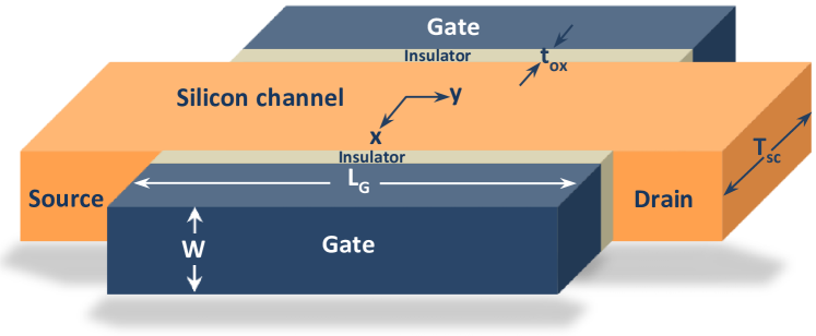
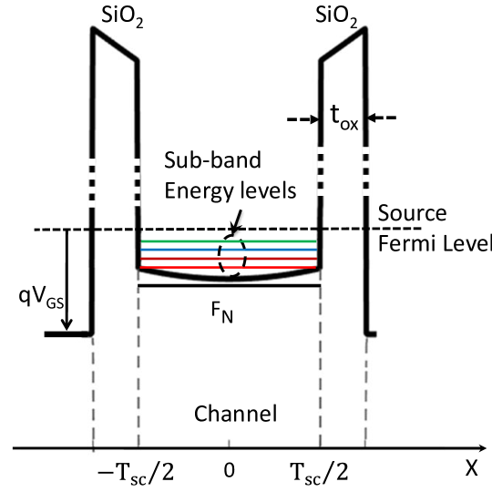
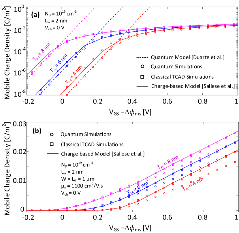
The structure of a n-type junctionless double-gate FET and the energy band diagram under a positive gate-to-source voltage is depicted in Fig. 1 and Fig. 2 respectively. The device parameters are listed in table I. The mode of operation of the JLFET can be either depletion, accumulation, or hybrid [1, 2]. When the whole channel operates in depletion, the gate-to-source voltage satisfies , where is the flat-band condition at the source given by . When the whole channel is in accumulation, , where is the flat-band condition at the drain given by . In between is the hybrid state where depletion and accumulation coexist (respectively towards the drain and the source). In Fig. 3, the mobile charge density obtained from the classical charge-based model in [1, 2] agrees with TCAD simulations when quantum corrections are neglected. However, the same model shows some mismatch when quantization is included. This is evidenced in ultra-thin channel layers (i.e. , and ) when TCAD simulations include quantum effect. Such quantum corrections were first introduced in [11], but still, the derivation was only valid in the subthreshold region. Moreover, Baccarani et. al [14] demonstrated that for ultra-thin channels, discrete sub-band energy states can be solved using a first order correction based on the time-independent perturbation theory of the Schrödinger equation. The discrete sub-band energy states were given as follows;
| (1) |
where and are respectively the sub-band number and valley number. For silicon with orientation, two valleys are considered. The lower valley twofold degenerated () with , and the higher valley fourfold degenerated () with ( is the free electron mass). The total semiconductor charge density per unit area is given by
| (2) |
where and are respectively the (quantized) mobile charge density and the fixed charge density per unit area. Despite relation (1) was obtained for lightly doped channels [14], its validity was demonstrated for highly doped channel JL devices[11] in the subthreshold region. In our model, we propose to use (1) also above the threshold.
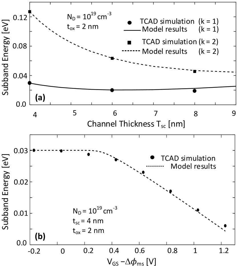
Fig. 4 (a) shows that the lowest subband energy level as a function of in the subthreshold region predicted by (1) closely follows numerical simulations. As illustrated in Fig. 4 (b), two regions of operation are evidenced. When the effective gate voltage is below V, the mobile charge density is negligible (see Fig 3 (b)), and the curvature of the potential well is dominated by the ionized donors, i.e. subband energies are gate voltage independent. When the effective gate voltage is above V, the negative mobile charge density becomes comparable to the positive fixed charge density and decrease with the gate voltage. This means that the curvature in the potential decreases, as for the correction of the ideal infinite quantum well. According to the model, the third term in RHS of (1) is proportional to , which is responsible for a decrease in subbands energy with an increase in the gate voltage. This is comparable to the reduction of subband energies upon widening of the effective potential well as reported in [15] for accumulation mode transistors. Fig. 4(b) also indicates that the first order correction proposed in [14] remains valid even above the threshold, including accumulation. The quantized mobile charge density per unit area, is the sum of charges in quantized sub-bands given by [14]
| Parameter | Symbol | Value |
|---|---|---|
| Channel Thickness | , , | |
| Channel Doping | ||
| Oxide Thickness | ||
| Channel Length | ||
| Channel Width | ||
| Work-function Difference | ||
| Electron Mobility | ||
| Silicon Permittivity | 11.68 | |
| Silicon Dioxide Permittivity | 3.9 |
| (3) |
where is the 2D effective density of states in the subband at energy and is the number of subbands. and are density of states effective masses for valleys and respectively [16]. is the electron quasi Fermi potential related to channel potential by
| (4) |
| Channel Thickness | Subband1 | Subband-2 | Subband-3 | Other Subbands |
|---|---|---|---|---|
| 78.4% | 15.9% | 4.6% | 1.1% | |
| 84.6% | 13.6% | 1.6% | 0.2% | |
| 94.8% | 5.15% | 0.04% | 0.01% |
where is conduction band edge at , is the central potential of the channel, is intrinsic carrier density and is the conduction band effective density of states. Under the assumption that only the first and second lowest sub-bands () concentrate most of the mobile charge density in practical situations, the contribution of higher sub-bands are ignored. The validity of this assumption is evident from table II. Combining (1), (2) and (3) with (4), a relation between , and is obtained:
| (5) |
Here, it is interesting to highlight that once the center potential is known, solving relation (5) gives the total charge density in the channel, and therefore the mobile charge density. As in [1, 2], the center potential still plays a key role in the model.
The next step is to introduce the Poisson equation in the model. To end with analytical expressions, we assume that the wave functions satisfy the Schrödinger equation for the infinite square quantum well, i.e. neglecting the band bending between the gates. This is a zero order perturbation in the wavefunction (still, the energy was corrected to the first order). As it will be evidenced later, this introduces negligible errors. In addition, for device thicknesses below we will consider only the two lowest sub-bands. To check the validity of this assumption, we calculated the percentage of the charge density including the first 10 sub-bands at the flat band condition () and found that the relative error in the carrier density is less than 6% for the channel thickness when using relations (1) and (3) (see table II). The mobile charge distribution obtained by weighting the first and second subband carrier densities and by the probability given by the wavefunctions and [14] writes
| (6) |
where is the wavefunction of energy state given by [17]
| (7) |
Recalling the Poisson equation
| (8) |
and integrating twice using from (7), then from (3) into (6), leads to an explicit relationship of the potential profile across the gates:
| (9) |
It should be remarked that , are internally linked to () according to (3), meaning that the problem now consists in finding the center potential () satisfying (3) and (9).
Importantly, relation (8) is not self-consistent with the potential , and in this sense relation (9) is approximate.
As a consequence, the contribution of the depletion charge to the electrostatic potential is discarded in this model. This means that the quadratic dependence of voltages with charges as stated in [1, 2] is not included, a simplification which is valid for the very thin channels at aim in this work.
III Charge-based approach
The boundary conditions arising from the continuity of the displacement vector at the interface must satisfy:
| (10) |
where is the potential at the surface of the channel and is oxide capacitance per unit area. Solving relation (9) at the Si-SiO2 interface , the surface potential is linked to the center potential through
| (11) |
where and corresponds to the first sub-band contribution to the mobile charge density, obtained by
| (12) |
where is the ratio of the first subband mobile charge density to the total mobile charge density, obtained from Table II.
Finally, merging (10), (11) and (12) links the total charge density to the center potential for a given value of :
| (13) |
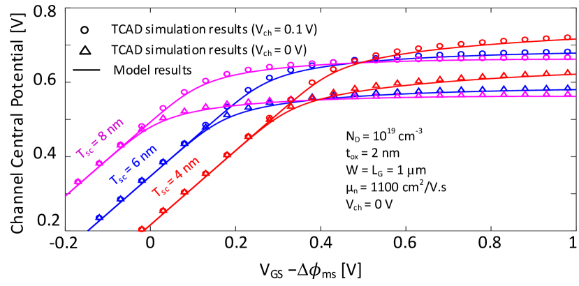
For fixed and quasi Fermi potentials (), relations (5) and (13) can be solved to obtain and . The channel center potential is plotted at the source () and the drain () with respect to the effective gate voltage in Fig. 5. For channel thickness, flat-band occurs at .
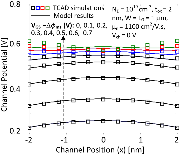
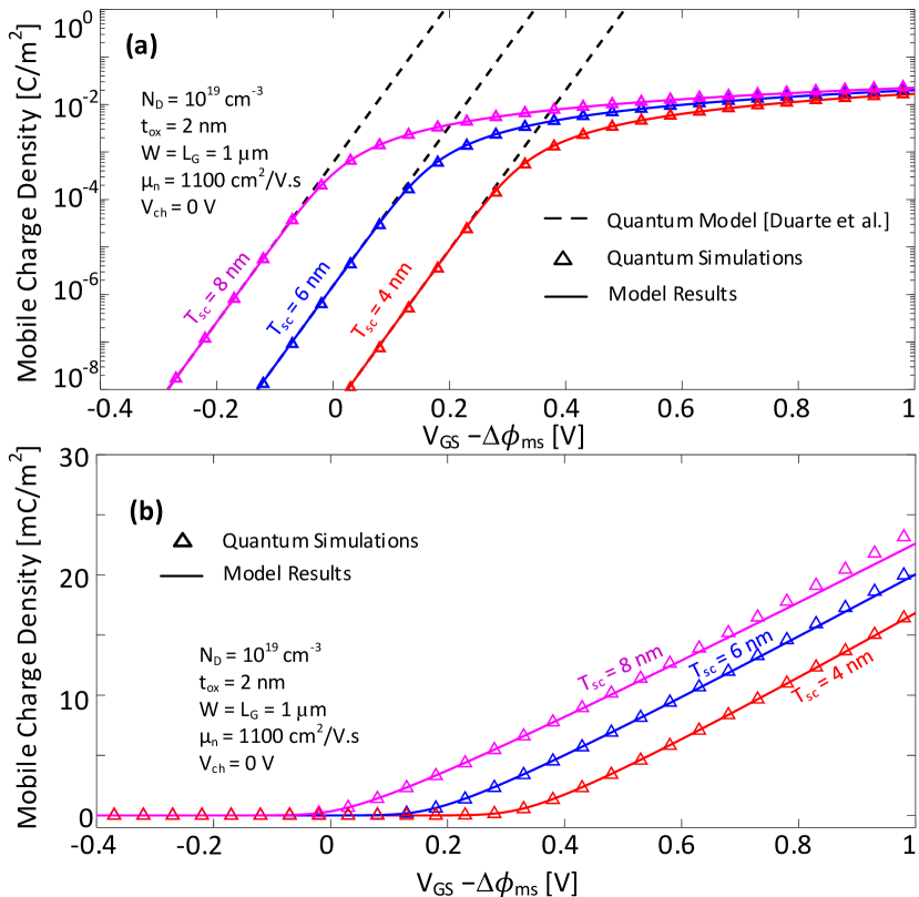
Fig. 6 compares the potential distribution across the channel for different values of . The model is accurate with respect to numerical simulation up to the flat-band voltage. For higher gate voltages, a small deviation is evidenced, most likely because of the large charge density that would ask for an additional correction of the wavefunctions (unlike for the energy states, wavefunctions are the solutions of the infinite square quantum well). The mobile charge density versus for different channel thicknesses is depicted on Fig. 7. The model matches TCAD simulations in all the regions of operation, both in linear and logarithmic scales (note that the derivation in [11] is accurate in deep depletion only). An approximation of the center potential can be further obtained from (5) when using the Boltzmann instead of the Fermi-Dirac statistics
| (14) |
It should be noted that at flat band, i.e. , depends on the thickness of the channel as indicated in Fig. 5 (in contrast to the classical limit where because quantum confinement still shifts the ground state in the channel and affects the flat band potential. If only the mobile charge density of the first subband is considered, while neglecting contributions from higher sub-bands , relation (5) can be simplified:
| (15) |
where is given by
| (16) |
Next, replacing from (15) in (13) leads to
| (17) |
| (18) |
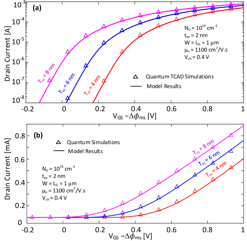
Fig. 7 confirms that the mobile charge density calculated from (17) with (5) and (13) is accurate for channel thicknesses of and . Concerning the 8nm-channel thickness, neglecting the second subband underestimates the mobile charge density in accumulation. Furthermore, for greater than nm, infinite quantum well with first order perturbation theory overestimates the first subband as illustrated in Fig. 4 (a). The electrostatic potential becomes more effective on the energy subbands [11] and either quantum harmonic oscillator (QHO) for subthreshold region or triangular QW for accumulation mode provide better approximations of the Schrödinger equation.
IV Drain Current Derivation
Relying on the drift-diffusion transport model, the total current is given by
| (19) |
where is the free carrier mobility and is corresponding to the Width of the device. The carrier mobility is assumed constant along the channel for the sake of simplicity.
Differentiating (17) gives in terms of and ;
| (20) |
Multiplying both side of (20) with and integrating once leads to
| (21) |
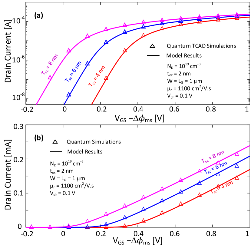
Finally, introducing (21) in (19), the total current is obtained from the semiconductor charge densities evaluated at source and drain. The current versus gate voltage is plotted in Fig. 8 and Fig. 9 for and respectively. The length and the width of the device are to avoid the short and narrow channel effects. The electron mobility was set to a constant value of . Bohm quantum potential (BQP) model calibrated with Poisson-Schrödinger model were used to predict electron transport in TCAD simulations. Using the same parameters as for TCAD simulations (i.e. no empirical parameters), the model predicts the current characteristics in all regions of operation with an accuracy of 93%.
In the classical limit, when the thickness of the channel increases so that the energy between subbands is comparable with , the series in (14) can be replaced by integral using the identity
| (22) |
where . Then, at the flat band condition (), the dependence on cancels in (14) and the classical definition of is recovered.
V Conclusion
We derived and discussed a charge based model for ultra-thin JL DG FET which takes into account charge quantization in all the regions of operation. The analytical solution introduces a zero order approximation in wave-functions and a first order correction for the confined energies. The model was validated with TCAD simulation for devices with channel thicknesses of 8 nm down to 4nm and shows high accuracy. This approach could be used as a core model for JLFETs implemented in Ultra Thin Body SOI technology.
References
- [1] J. M. Sallese, N. Chevillon, C. Lallement, B. Iniguez, and F. Pregaldiny, “Charge-based modeling of junctionless double-gate field-effect transistors,” IEEE Transactions on Electron Devices, vol. 58, no. 8, pp. 2628–2637, Aug 2011.
- [2] F. Jazaeri and J.-M. Sallese, Modeling Nanowire and Double-Gate Junctionless Field-Effect Transistors. Cambridge University Press, 2018.
- [3] Jean-Pierre Colinge, Chi-Woo Lee, Aryan Afzalian, Nima Dehdashti Akhavan, Ran Yan, Isabelle Ferain, Pedram Razavi, Brendan O’Neill, Alan Blake, Mary White, Anne-Marie Kelleher, Brendan McCarthy, and Richard Murphy, “Nanowire transistors without junctions,” Nature Nanotechnology, vol. 5, pp. 225–229, February 2010.
- [4] C.-W. Lee, A. Afzalian, N. D. Akhavan, R. Yan, I. Ferain, and J.-P. Colinge, “Junctionless multigate field-effect transistor,” Applied Physics Letters, vol. 94, no. 5, p. 053511, 2009.
- [5] R. T. Doria, M. A. Pavanello, R. D. Trevisoli, M. de Souza, C. W. Lee, I. Ferain, N. D. Akhavan, R. Yan, P. Razavi, R. Yu, A. Kranti, and J. P. Colinge, “Junctionless multiple-gate transistors for analog applications,” IEEE Transactions on Electron Devices, vol. 58, no. 8, pp. 2511–2519, Aug 2011.
- [6] C.-W. Lee, A. Afzalian, N. D. Akhavan, R. Yan, I. Ferain, and J.-P. Colinge, “Junctionless multigate field-effect transistor,” Applied Physics Letters, vol. 94, no. 5, p. 053511, 2009.
- [7] F. Jazaeri, L. Barbut, A. Koukab, and J.-M. Sallese, “Analytical model for ultra-thin body junctionless symmetric double gate mosfets in subthreshold regime,” Solid-State Electronics, vol. 82, pp. 103 – 110, 2013.
- [8] F. Jazaeri, L. Barbut, and J. M. Sallese, “Generalized charge-based model of double-gate junctionless fets, including inversion,” IEEE Transactions on Electron Devices, vol. 61, no. 10, pp. 3553–3557, Oct 2014.
- [9] Farzan Jazaeri and Lucian Barbut and Jean-Michel Sallese, “Trans-capacitance modeling in junctionless symmetric double-gate mosfets,” IEEE Transactions on Electron Devices, vol. 60, no. 12, pp. 4034–4040, Dec 2013.
- [10] F. Jazaeri, L. Barbut, and J.-M. Sallese, “Modeling and design space of junctionless symmetric dg mosfets with long channel,” IEEE Transactions on Electron Devices, vol. 60, no. 7, pp. 2120–2127, July 2013.
- [11] J. P. Duarte, M. S. Kim, S. J. Choi, and Y. K. Choi, “A compact model of quantum electron density at the subthreshold region for double-gate junctionless transistors,” IEEE Transactions on Electron Devices, vol. 59, no. 4, pp. 1008–1012, April 2012.
- [12] S. Gupta, B. Ghosh, and S. B. Rahi, “Compact analytical model of double gate junction-less field effect transistor comprising quantum-mechanical effect,” Journal of Semiconductors, vol. 36, no. 2, p. 024001, 2015.
- [13] M. Chanda, S. De, and C. K. Sarkar, “Modeling of characteristic parameters for nano-scale junctionless double gate mosfet considering quantum mechanical effect,” Journal of Computational Electronics, vol. 14, no. 1, pp. 262–269, Mar 2015.
- [14] G. Baccarani and S. Reggiani, “A compact double-gate mosfet model comprising quantum-mechanical and nonstatic effects,” IEEE Transactions on Electron Devices, vol. 46, no. 8, pp. 1656–1666, Aug 1999.
- [15] J.-P. Colinge, A. Afzalian, C.-W. Lee, R. Yan, and N. D. Akhavan, “Influence of carrier confinement on the subthreshold swing of multigate silicon-on-insulator transistors,” Applied Physics Letters, vol. 92, no. 13, p. 133511, 2008. [Online]. Available: https://doi.org/10.1063/1.2907330
- [16] Y. Taur and T. H. Ning, Fundamentals of Modern VLSI Devices, 2nd ed. Cambridge University Press, 2009.
- [17] P. Harrison and A. Valavanis, Quantum Wells, Wires and Dots: Theoretical and Computational Physics of Semiconductor Nanostructures. Wiley, 2016.
![[Uncaptioned image]](/html/1808.06685/assets/Majid.png) |
Majid Shalchian received the Ph.D. degree in electrical engineering (microelectronics) from Sharif University of Technology, Tehran, IRAN, in 2005.He joined Amirkabir University of Technology (Tehran Polytechnique), as assistant professor in electrical engineering department. His current research interests include semiconductor device modelling and parameter extraction as well as VLSI circuit design. He is the director of VLSI Laboratory and advanced automotive electronics Laboratory in Amirkabir University of Technology. |
![[Uncaptioned image]](/html/1808.06685/assets/Farzan.png) |
Farzan Jazaeri received the Ph.D. degree in microelec tronics and microsystems from the Ecole Polytechnique Fédérale de Lausanne (EPFL), Lausanne, Switzerland, in 2015. He joined the Integrated Circuits Laboratory, EPFL, as a Research Scientist and a Project Leader. His current research interests include solid state physics and advanced semiconductor devices for operation within extreme harsh environments, i.e., high energy particle background and cryogenic temperatures for space applications and quantum computations. |
![[Uncaptioned image]](/html/1808.06685/assets/Sallese.png) |
Jean-Michel Sallese received the Ph.D. degree in physics from the University of Nice Sophia Antipolis, Nice, France. He joined the Ecole Polytechnique Fédérale de Lausanne, Lausanne, Switzerland, and was appointed as the Maitre d’Enseignement et de Recherche. His group (Electron Device Modeling and Technology Laboratory ) has dedicated attention to the solid state physics and modeling of field-effect transistors, radiation damages in integrated circuits collaboration with CERN, and heterostructure HEMT devices. |