(0cm,2cm)\hrefhttps://doi.org/10.1109/TBCAS.2018.2881219DOI: 10.1109/TBCAS.2018.2881219, © 2018 IEEE. The article has been accepted for publication.
Inter-IC for Wearables (I2We): Power and Data Transfer over Double-sided Conductive Textile
Abstract
We propose a power and data transfer network on a conductive fabric material based on an existing serial communication protocol, Inter-Integrated Circuit (I2C). We call the proposed network inter-IC for wearables (I2We). Continuous dc power and I2C-formatted data are simultaneously transferred to tiny sensor nodes distributed on a double-sided conductive textile. The textile comprises two conductive sides, isolated from each other, and is used as a single planar transmission line. I2C data are transferred along with dc power supply based on frequency division multiplexing. Two carriers are modulated with the clock and the data signals of I2C. A modulation and demodulation circuit is designed such that off-the-shelf I2C-interfaced sensor ICs can be used. The novelty of this work is that a special filter to enable passive modulation is designed by locating its impedance poles and zeros at the appropriate frequencies. The term “passive modulation” herein implies that the sensor nodes do not generate carrier waves by themselves; instead, they reflect only the externally supplied careers for modulation. The proposed scheme enables the flexible implementation of wearable sensor systems in which multiple off-the-shelf tiny sensors are distributed throughout the system.
Index Terms:
Body sensor networks, e-textiles, frequency division multiplexing, serial communication, wearable networks.I Introduction
Smart fabrics, or e-textiles [1], that can perform biomedical sensing on a user’s body surface while eliminating a number of individual wires is a key technology for wearable health monitor systems. Distributing various sensors throughout for temperature measurement, accelerometers, electrocardiography/electromyography, etc., will yield rich information for health care [2] and is applicable to human–computer interfaces [3].
Powering the distributed sensors and gathering the sensor readings on the system are critical for implementing such wearable sensor systems. Although functionalizing a fiber itself, e.g., piezoelectric fibers [4, 5] and strain-sensing fibers [6, 7], is a promising approach to embed sensors into clothing without sacrificing comfort, an entire system still requires some silicon-based circuit components to include amplifiers and digital communication interfaces. Therefore, the integration of textiles and silicon-based circuitry, which are produced separately, is required to build a complete wearable sensing system. The motivation of this work is to present a practical method to integrate off-the-shelf silicon-based sensors and textiles.
One modern, straightforward approach is radio-based wireless communication. Each sensor operates with a tiny battery and sends data over the air. However, frequent data transmission by densely distributed sensors will involve significant difficulties including interference, latency, and battery life.
Another approach to avoid these difficulties is wire-based communication. For the physical connection in wearable systems, circuit patterning on fabric with conductive yarns [8, 9], conductive screen printing ink [10, 11], or ironed-on conductive fabric patches [12], instead of copper tracks on conventional printed circuit boards (PCBs), is a straightforward and practical approach. This approach requires separate conductive lines connecting the leads/pads of electronic components individually, as in conventional PCBs. A possible vulnerability is that the fraying/whiskering of the fabric would cause a fatal breakdown, such as the disconnection of tracks and short-circuit between neighboring conductive tracks.
An alternative approach to such one-to-one wiring is by connecting all the devices on the clothing with a single bus. A double-sided conductive fabric sheet, i.e., both sides of the sheet are conductive and are insulated from each other, can be used as the bus [13, 14, 15, 16, 17, 18].
The most significant advantage of this approach is that the conductive textile is patterned uniformly without depending on the sensor node locations. Therefore, the textile and electronic circuitry can be designed and fabricated independently from each other. The same textile is typically used in various products and is cost effective. Because the sensor nodes do not require being located precisely on the textile, they can be detached and reassembled in daily use; subsequently, the wear is washable even if the sensors are not waterproof. It is noteworthy that the uniform pattern is not mandatory, and any other artwork patterns with conductive yarns/ink can be used if they are preferred.
As a simple implementation using commercially available iButton [19] devices, the MicroLAN [20] sensor network on a layered conductive fabric has been presented in [13]. TextileNet [15] enables a dc power supply and serial communication on the transmission line by temporally switching the power supply state and the pulse transfer state; thus, the power supply is intermittent and only a singleplexed signal transfer is supported. Wade and Asada proposed a dc powerline communication on a layered conductive textile [21, 14], using a modulation/demodulation (modem) circuitry developed by themselves [22]. A continuous dc power supply and amplitude modulated signal using a carrier in a frequency range of 2–10 MHz are transferred simultaneously on the same textile medium. Based on a similar concept, continuous dc power supply combined with multiplexed signal transfer [18] derived from multiplexed ac power transfer [17], have been presented, based on frequency division multiplexing (FDM). In those works, the three-channel on/off control of slave devices was demonstrated by the on-off modulation of three carriers. This scheme requires carriers at different frequencies to achieve -channel on-off control, i.e., -bit signal transfer.
Herein, the FDM scheme is utilized to transfer a pair of clock and data signals of a serial communication protocol, i.e., Inter-Integrated Circuit (I2C) [23]. It provides compatibility with a significantly wider range of commercially available sensor ICs and microcontrollers (MCUs), compared with iButton devices or specially designed modems presented in the previous works mentioned above.
The primary contribution of this study is the proposal of inter-IC for wearables (I2We) that combines I2C data transfer and dc power supply on a double-sided conductive textile. As illustrated in Fig. 1, the dc power and I2C signals are transferred simultaneously on the same planar transmission line using FDM, similar to other PLCs [22, 24, 25].
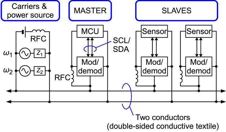
An important advantage of the proposed method is the small footprint and low power consumption achieved by passive modulation. I2C-interfaced ICs send the output data by modulating the carriers supplied externally, similar to passive radio frequency identification (RFID) [26] and other backscatter communications [27, 28, 29]. Indeed, the modulation operation relies on an “active” digital IC; the term “passive modulation” herein implies, nonetheless, that the carrier generator is separated from the modulation circuitry and eliminated from each tiny sensor node. A specially designed LC filter, described in Section III, enables the passive modulation. The filter design considering the location of its impedance poles and zeros at appropriate frequencies is the novelty of this work. The theoretical analysis on the filter design and comparison with simulation/experiment are additional contributions of this paper to our previous conference paper [30]. The carriers are modulated directly with the I2C interface outputs of a digital IC, and also demodulated with a simple carrier detector and a data slicer without any additional digital signal processor or buffer memories.
Contrary to conventional radio links, the proposed I2We link can eliminate the latency due to listen-before-talk, and collision followed by retransmission. In radio-based wireless sensor networks, such latency causes the out-of-order arrival of data from distributed sensor nodes, and disturbs processing such as sensor fusion at the sink node. To recover the order of the data as they are acquired by sensors, a time base must be shared in the sensor network for time stamping, in which additional resources are required on each node. In an I2We network, as well as I2C, the master fully initiates data transfer transactions and receives sensor data in order; therefore, no additional processing for data ordering is required.
Another important feature from a practical viewpoint is, as stated above, that the I2We network is implemented with off-the-shelf I2C-enabled ICs and MCUs. Engineers familiar with the I2C network can easily reuse the same ICs and MCUs, as well as software libraries implemented in MCUs. Additionally, some of the commercially available low-cost sensor ICs, e.g., inertial measurement units (IMUs), provide well-engineered sensor fusion functionalities integrated into a single chip. I2We enables reusing such functions and provides an option to avoid reinventing the same functionalities.
I2We enables sensor-distributed clothing. Potential applications include distributed body temperature sensors for medical monitoring/diagnosis [31], and distributed posture sensors for motion analyses in rehabilitation [32]. Multimodal sensing systems can also be implemented, because various types of I2C-interfaced sensors can coexist on the same clothing.
The remainder of the paper is organized as follows. Section II briefly describes the structure of a double-sided conductive textile and a tack connector. Section III explains the operation principle of the proposed I2We network. A design example and a demonstration system are presented in Section IV and Section V, respectively. Finally, conclusions are presented in Section VI.
II Double-sided Conductive Textile
This section briefly describes the double-sided conductive textile and a tack connector used in this work. The proposed I2We communication is applicable to any two-conductor transmission lines including coaxial, twisted-pair, and parallel-pair cables. Nonetheless, combination with a double-sided conductive textile would be suitable for wearable systems, because it provides the freedom of sensor location along with a lower resistance and higher current capacity, while using a fairly flexible conductive textile for comfortable wearability. The advantages of such two-dimensional (2-D) conductive material over a one-dimensional (1-D) conductive strand are discussed in detail in [14]. The resistance between two points on the 2-D material is approximately proportional to the logarithm of the distance between the two points, while the resistance of a 1-D conductor is proportional to its length. In this work, we assume that the resistance is almost frequency independent, because the silver plating thickness of the conductive yarns is significantly smaller than the skin depth at the carrier frequencies used in this work. The resistance is also stable with respect to the deformation of the textile. Additionally, on the 2-D material, the current paths are redundant, and the connection is retained robustly even if the material is partially damaged.
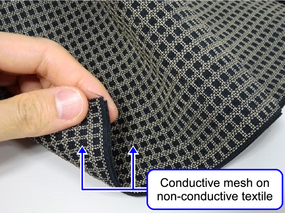
An example of the textile is shown in Fig. 2. The base textile is nonconductive; further, on both of its sides, square mesh patterns are embroidered with conductive yarns. A cross-sectional view of the structure is illustrated in Fig. 3. The conductive yarns on one side are electrically connected together and isolated from the conductive mesh on the other side. The square mesh is not mandatory and any other artwork patterns can be used. Alternately, conductive yarns can be integrated at the stage of the textile fabrication, i.e., the textile can be woven/knitted with both conductive and nonconductive yarns. Piling up conductive and nonconductive textile sheets or printing conductive ink on both the sides of a nonconductive base textiles sheet are also acceptable. Regardless of the fabrication method, an essential requirement is that the conductive materials are exposed on both sides, and both the conductive surfaces are isolated from each other.
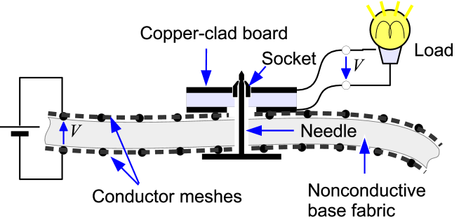
As shown in Fig. 3, a special connector consisting of a tack (needle) and a socket is used in this work. The back side of the PCB is in direct contact with one side of the textile, and the conductive needle-and-socket connector enables the electrical connection between the PCB and the other side of the textile. To avoid shorting both conductive surfaces, the needle should be partially insulated or placed in a nonconductive area, i.e., inside an aperture of the mesh. This configuration allows for the physical mounting of a device, and its electrical connection to be integrated into a single action, i.e., sticking the needle through the textile and mating the needle with the socket. The pinching of the textile induces only a negligible effect on the impedance of the textile.
The voltage applied between the two conductive planes will also be applied to the user’s body, if the user touches both naked conductive surfaces simultaneously. Provided that the voltage is as low as the standard power rail voltage for modern digital circuitry, such as 3.3 V, the voltage will not be harmful for the user. Nonetheless, if the system is required to avoid applying the voltage on the user’s body, the conductive surfaces must be covered with the appropriate insulation layers.
III Principle of Operation
III-A Inter-Integrated Circuit (I2C)
This subsection briefly explains the operation and implementation of the I2C. The descriptions below assume the standard mode or fast mode, with clock frequencies up to 100 kHz or 400 kHz, respectively, defined in the I2C specification [23].
An I2C bus consists of two signal lines: clock (SCL) and data (SDA). One or more masters, and one or more slaves can be connected to the bus in parallel. Only one master can initiate the communication at a time, and all the other slaves on the bus listen to the master’s signal; subsequently, only a slave addressed by the master responds to the signal during the transaction. The bus is bidirectional, i.e., the data can be transferred from the master to the slave, and vice versa. For both directions, the master generates the clock signal, and thus initiates the communication. The data signal is generated by the master or the slave, depending on the master’s transmit mode or receive mode.
An I2C bus configuration including the output transistors inside the master and the slave is shown in Fig. 4.

The SCL and SDA pins of each node are bidirectional and are connected internally to an input circuitry and an open-drain transistor output. The digital input circuitry draws only a negligible current. The SCL and SDA lines are pulled up individually to the positive supply voltage with resistors. While no signal is transferred on the bus, all the output transistors are in the off state, and the SCL/SDA lines are nearly at the positive supply voltage, i.e., the logical high. When any one of the output transistors is turned on, the signal line is inverted nearly to the ground level, i.e., the logical low.
It is noteworthy that the output pins only sink the current, but do not actively source the current. The dc voltage required to interpret the transistors’ off/on states to logical high/low levels is supplied externally.
III-B Clock and Data Multiplexing on Conductive Textile
As described in Section II, a single transmission line is formed with a double-sided conductive textile. In this work, the SCL/SDA signals and dc power supply are transferred simultaneously on the same transmission line using FDM. For SCL/SDA transmission, two frequency carriers are modulated respectively with SCL and SDA, in the form of amplitude shift keying (ASK).
The proposed I2We bus configuration including the output transistors inside the master and the slave is shown in Fig. 5.
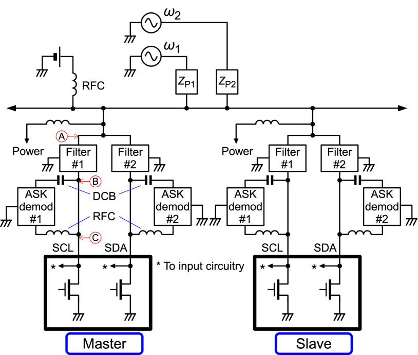
Similar to the external dc supply to the signal lines via the pull-up resistors in conventional I2C, the RF carriers are supplied externally to the bus via “pull-up” impedances. The carrier generator can be separated from the master and the slave. The SCL and SDA pins of each node are connected to the bus through special bandpass filters, and the output transistors’ off/on states are interpreted directly into high/low states in the RF carrier amplitude on the signal line. In each of the master and the slave, the amplitude shift is interpreted as logical high/low levels by the ASK demodulation circuitry. Thus, the SCL/SDA pins of an off-the-shelf I2C-enabled ICs modulate the carriers directly and receive digital SCL/SDA signals via the demodulation circuitry.
III-C Filter Design for Passive Modulation
In this subsection, the ASK modulation operation and the filter design to achieve the operation are described in detail.
The basic idea for passive ASK modulation in the configuration shown in Fig. 5 is, similar to the conventional I2C, to switch the impedance connected to the signal line between open and short, depending on the logical state of the SCL/SDA pin. To modulate two carriers independently, the impedance element should achieve an open/short switch at the frequency of the carrier to be modulated, and should remain open at the other frequency.
An equivalent circuit that represents one of the two (SCL and SDA) signal inputs/outputs (I/Os), its associating filter, and a carrier source is illustrated in Fig. 6. It is noteworthy that the model includes the parasitic impedance associated with both the input circuitry and output transistor of the I/O. Although the input impedance at the logical high-state, , draws only a negligible current at the frequency of the digital signals, it is not negligible at the carrier frequencies. The capacitance is not neglected, but rather intentionally utilized for the filter resonance.
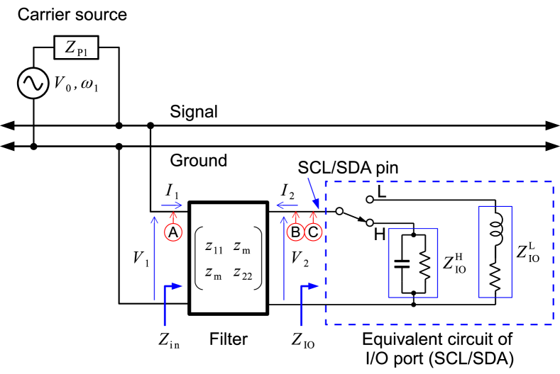
We define the impedance matrix of the reciprocal two-port filter as follows:
| (1) |
where and are the voltages across ports 1 and 2, respectively; and are the currents flowing into ports 1 and 2, respectively.
The secondary port is connected to the SCL/SDA pin. Let denote the input impedance of the SCL/SDA pin; subsequently
| (2) |
From (1) and (2), the impedance looking into the filter at the primary port, , is calculated as follows:
| (3) |
Thus, the filter fs primary port impedance depends on , which is determined by the on/off-state of the open-drain transistor, i.e., the logical high/low output. Let and represent the impedances of the I/O at the logical high and low states, respectively. While the carrier with a constant voltage amplitude is supplied via a pull-up impedance , the voltage appearing at the primary port of the filter is calculated as follows:
| (4) |
From (3) and (4), is determined by depending on . Thus, the carrier is ASK modulated directly depending on the logical output of the SCL/SDA pin. The filter for modulating the carrier should maintain a high impedance at , regardless of the logical pin state.
The requirements on to modulate the carrier and to avoid the cross-talk modulation of the carrier are as follows:
-
1.
For the logical high-state, should be open, to avoid a decrease in the joint impedance of all the filters connected to the same transmission line.
-
2.
For the logical low-state, should be short, to achieve a higher modulation depth for clearly distinguishable symbols.
-
3.
Regardless of the logical state, should be open, to avoid cross-talk modulation.
The requirements above are summarized in Table I.
| 1) | 2) | |
| 3) | 3) |
1), 2), 3): Correspond to the enumerated items in the body text.
Suppose that the filter consists of lossless, passive reactances. All the elements of the impedance matrix in (1) are therefore pure imaginary numbers. Subsequently, the impedance matrix is realized with a T-network shown in Fig. 7, where the reactance on each branch is defined as follows:
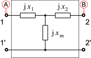
| (5) | ||||
| (6) | ||||
| (7) |
The three elements in the T-network are determined by considering the requirements, as described below.
Because the I/O pin is a parallel network of the digital input circuitry and the open-drain transistor in the off-state, is an almost pure capacitive reactance, i.e.,
| (8) |
where is a positive real number.
The first requirement stated above, for the logical high state, can be satisfied if and in (3). Therefore, is expressed as follows:
| (9) |
which is a pure inductive reactance.
The second requirement, for the logical low, is achieved by . This can be approximated as , because . Therefore,
| (10) |
By substituting (9), (6) and (10) are respectively rewritten as follows:
| (11) |
and
| (12) |
The relationship among , and , and combinations of the inductive/capacitive reactances satisfying the equations above are shown in Fig. 8.
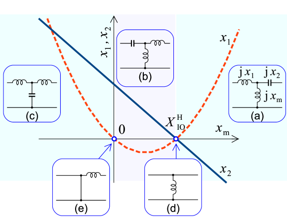
For the third requirement, to stop the current from flowing through the filter fs primary port regardless of the logical state of the I/O pin, an LC parallel resonant network should be placed at the -branch. The joint impedance of a parallel connection of inductance and capacitance , satisfying , at is calculated as follows.
| (13) |
where . Thus, is inductive for , and is capacitive for . An appropriate configuration should be chosen depending on . For example, is inductive in configuration (a) shown in Fig. 8; therefore, this configuration is applicable only to the condition . Meanwhile, for , configuration (b) is applicable.
To summarize the discussions above, the minimal filter configurations are listed in Table II.
| (a) | (b) | (c) | (d)-1 | (d)-2 | |
|---|---|---|---|---|---|
| Frequency condition | |||||
| Configuration |
|
|
|
|
|
|
Equivalent circuit
at |
|
|
|
|
|
|
Equivalent circuit
at |
|
|
|
|
|
(a), (b), (c), and (d) on the top row of the table correspond to those in Fig. 8. Configuration (d), in which , is realized by series resonance at the -branch. The additional reactance element connected in series to the parallel LC is inductive or capacitive, depending on . Configuration (e) shown in Fig. 8 is inappropriate and is therefore excluded from the table, because all of the current flowing into the filter from the primary port flows through and no current appears at the secondary port.
III-D ASK Demodulator
To interpret the carrier amplitude shift into a logical high/low that is comprehensive for the digital IC, an ASK demodulator is required for each SCL/SDA pin, as shown in Fig. 5.
The demodulator input is ac-coupled with a capacitor, and the output is RF-decoupled with an inductor. Therefore, the demodulator operates without any positive/negative feedback effects such as oscillation and self-holding, although the input and output are connected to the same SCL/SDA pin.
A block diagram of the demodulator is shown in Fig. 9.

The carrier is fed into the RF detector via the filter described in the previous subsection, and the carrier is blocked by the filter. The RF detector extracts the envelope of the carrier. The analog envelope waveform is binarized by a data slicer [33]. The data slicer tunes the reference voltage of the comparator automatically depending on the input waveform, via a lowpass filter (LPF). The binary output of the data slicer is accepted by the SCL/SDA pin. The comparator output terminal should be RF-decoupled from the filter and the SCL/SDA pin using an RF choke (RFC), such that the comparator output impedance does not affect the filter design.
IV Design Example
This section presents an example of the I2We system design. It is noteworthy that it is only an example, and is not an optimized design.
IV-A Carriers and I/O Capacitance
To design the filters, the carrier frequencies and the capacitance of the SCL/SDA pins must be specified.
We choose the carrier frequencies of 20 MHz and 50 MHz for the SCL and SDA, respectively. The two frequencies should avoid being an integer multiple of each other, to minimize crosstalk due to harmonics. The lower bound of the carrier depends on the frequency of the SCL signal. For the standard mode with 100-kHz SCL, the carrier frequencies are required to be significantly higher than 100 kHz. The upper bound is determined such that the wavelength in the textile medium is significantly longer than the size of the textile. If the wavelength is comparable to or shorter than the size of the textile, the carrier signal strength at each receiver depends primarily on the location and frequency, because of the standing waves. The received signal strength fluctuation requires a more complicated configuration of the demodulator.
In this work, we used a development board called Teensy 3.2 [34] with a 32-bit MCU, MK20DX256VLH7 [35]. The measured capacitance of the SCL/SDA pin of the MCU, including the stray capacitance of PCB copper tracks, was approximately 8 pF at the logical high state. For the carrier frequencies 20 MHz and 50 MHz, the reactance of the capacitance is approximately k and , respectively.
IV-B Filter Design
As discussed in Section III-C, The filter configurations should be selected from those shown in Table II. Here, we choose (a) and (b) for the lower carrier (20 MHz) and higher carrier (50 MHz), respectively.
The theoretical analyses of the filter presented in the previous section assumed lossless reactance components. A one degree of freedom exists and can be determined arbitrarily to satisfy in (a) and in (b). For the actual filter design, the one degree of freedom enables the appropriate inductors and capacitors to be chosen such that the filter possesses a significantly high/low impedance to achieve the characteristics shown in Table I. The highest/lowest impedance that can be achieved by the filter depends on the specific characteristics of the inductors and capacitors, including the loss factors.
One significant factor that dominates the filter characteristics is the frequency of the impedance zero between two impedance poles. When the SCL/SDA pin is at the logical high state, two poles of are required to be located at and . From Foster’s reactance theorem [36], there is an impedance zero at , where for configuration (a) and for (b). The zero should be separated from the two poles on the frequency axis, because a pole can be almost canceled by the closely located zero, and the impedance magnitude will be reduced significantly . The frequency of the impedance zero can be tuned with .
The filter configurations including the equivalent impedance of the SCL/SDA pins are shown in Table III. An example of the selection of inductors and capacitors is shown in Table IV; it includes the exact values calculated with (11) and (12) and approximated values selected from the E12 series. is increased by adding an external shunt capacitor in configuration (a) to reduce the inductance of such that the inductor can be chosen from commercially available high-Q wire-wound tiny chip inductors, which are typically lower than 10 H at the maximum. Terminals 1-1’, 2-2’, and 1-2 are required to be isolated at dc; therefore, dc block (DCB) capacitors are inserted as shown in Table III. The impedance of the DCBs at the carrier frequencies are negligible.
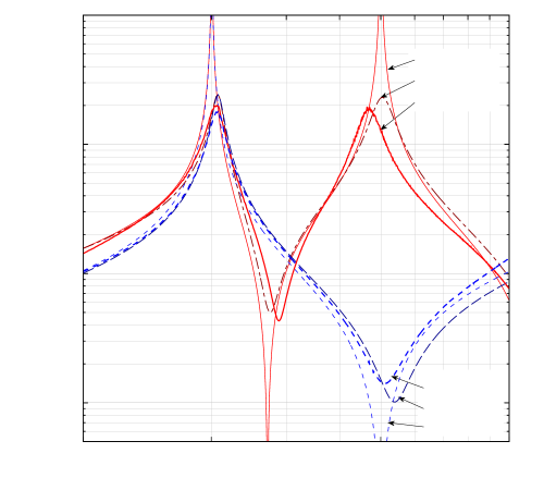
The simulated impedance–frequency curves of the designed filters are presented in Fig. 10. The simulations were performed with LTspice XVII. The simulation results for both lossless and lossy models are plotted. The lossless simulations were conducted with the exact calculated inductances/capacitances in Table IV. Additionally, was replaced with an open circuit and was replaced with a short circuit. For lossy simulations, we used the E12 series values and manufacturer-supplied inductor SPICE models [37] that represent the realistic characteristics well, including the losses and self-resonance. The capacitors were modeled as ideal capacitances because their loss factors are negligible compared with the inductors at the frequencies of interest. Based on our preliminary measurement results, we chose k and for the lossy models. The result indicates that the lossless models achieve the ideal open and short at the carrier frequencies, and that the lossy models achieve significant impedance changes of more than two orders of magnitude at .
| (a) | (b) | |
|---|---|---|
| Frequency condition | ||
| Configuration |
![[Uncaptioned image]](/html/1808.06548/assets/x25.png)
|
![[Uncaptioned image]](/html/1808.06548/assets/x26.png)
|
|
Equivalent circuit
at for logical high |
|
|
|
Equivalent circuit
at for logical low |
|
|
represents parallel connection of and .
\makebox(0.0,0.0)[]{{}}
| (a) | (b) | ||||
|---|---|---|---|---|---|
| Calculated | E12 series | Calculated | E12 series | ||
| 18 pF (8 pF 10 pF∗) | 8 pF | ||||
| 4.7 H | 1.0 H | ||||
| 1.33 H | 1.2 H | 1.10 H | 1.0 H | ||
| 7.64 pF | 8 pF | 57.3 pF | 56 pF | ||
| 53.6 pF | 56 pF | 0.267 H | 0.22 H | ||
* An external shunt capacitor is added.
The filters (a) and (b) were fabricated as shown in Fig. 11, and their input impedances were measured with a vector network analyzer (VNA) of Agilent Technologies E5071B. The measurement results shown in Fig. 10 agree reasonably well with the simulation results of the lossy models. Let and denote at the logical high and low states, respectively. is approximately 44 at 20 MHz for filter (a), and 87 at 50 MHz for (b).
In Fig. 6, let and denote the voltage across the primary port of the T-filter at the logical high and low states, respectively. The ratio determines the maximum ratios of to . When the carrier is supplied from a voltage source via a pull-up impedance , is calculated from (4) as follows.
| (14) |
If is significantly greater than and ,
| (15) |
Thus, the ratio (15) can achieve 44 and 87 at the maximum, for the SCL and SDA, respectively. However, the supplied carrier voltage attenuates significantly with . must be tuned according to the carrier source voltage and RF detector sensitivity.
The ratio that determines the ASK modulation depth can be represented by (15) provided that only a single set of modulation circuitry is connected to the bus. When modules are connected in parallel and modules maintain a high-impedance state during the modulation operation of a single module, (15) is revised as follows:
| (16) |
where represents parallel connection. For ,
| (17) |
For , dB. Hence, the maximum number of the modules that can operate on the same bus depends on and the demodulator characteristics.
IV-C ASK Demodulator Design
A design example of the ASK demodulator is shown in Fig. 12.
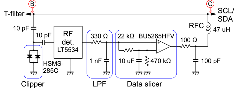
The secondary port of the T-network filter is connected to the input of an RF detector via DCB capacitors. The envelope of the RF signal is detected and is fed to a data slicer via a low pass filter (LPF).
Although the DCB and RFC suppress feedback from the slicer output to the detector input as explained in Section III-D, a transient voltage spike is induced at the detector input when the logic level of the SCL/SDA pin is toggled and stimulates the RF detector. This can cause the latch-up of the data slicer output as follows. When the RF amplitude shifts to the low level, the RF detector output decreases, and the data slicer output turns to low. The voltage step from the high to low level causes the voltage spike at the RF detector input described above; subsequently, the detector output increases again, and the data slicer output becomes high. Thus, the slicer output holds the logical high, regardless of the actual RF amplitude. To prevent the latch-up fault, an anti-parallel diode pair is connected to the input of the detector. The diodes clip off the spike at , where denotes the forward voltage drop of the diode. The desired RF signals and are detected accurately across the diodes, because the voltage amplitude of the RF signal is smaller than .
For the RF detector, LT5534 of Linear Technology was used. It is a log-scaled RF detector with the output slope of 44 mV/dB at 50 MHz and the input impedance of 2 k [38]. The high input impedance is desirable to reduce the change in the impedance that is connected to the secondary port of the T-filter. A relatively small DCB capacitance that is a series connection of two 10-pF capacitors was used to further increase the impedance.
The data slicer can be composed with general comparator ICs that operate with a bandwidth that is significantly greater than the SCL frequency, typically 100 kHz. In this example, Rohm BU5265HFV [39] was used. The resistor at the data slicer output is for limiting the shoot-through current. Although the slicer output and the SCL/SDA pin hold the same logical level, they can cause a discrepancy for a short period at a transition of the logical state and cause a shoot-through current. The capacitor connected to the resistor and the RFC is for the stabilization of the RF impedance looking into the demodulator from the output terminal, regardless of the logical state of the output.
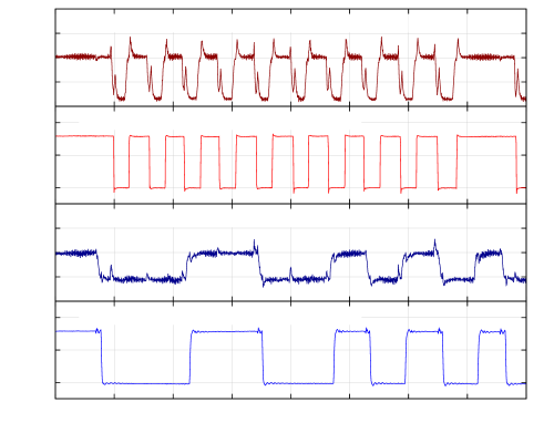
A modem module PCB was fabricated as shown in Fig. 13. A pair of filters and a pair of demodulators for the SCL and SDA were integrated into a single PCB. The measured waveforms on this module are shown in Fig. 14. In the measurement, 20-MHz and 50-MHz carriers of approximately 10–20 mV amplitude were supplied to the textile, and they were modulated with another modem module connected to the SCL/SDA ports of a Teensy 3.2 MCU board. To clearly distinguish the baseband and carrier signals at the demodulator, their frequencies should be apart from each other by at least 1–2 orders of magnitude. For the power supply, a 3.3-V dc voltage was also applied to the textile via an RFC inductor.
\makebox(0.0,0.0)[]{{}}
\makebox(0.0,0.0)[]{{}}
\makebox(0.0,0.0)[]{{}}
\makebox(0.0,0.0)[]{{}}
\makebox(0.0,0.0)[]{{}}
\makebox(0.0,0.0)[]{{}}
\makebox(0.0,0.0)[]{{}}
\makebox(0.0,0.0)[]{{}}
V Demonstration System
This section presents a demonstration system. The master device collects sensor readings from multiple sensor nodes, and the data are visualized on a PC, as shown in Fig. 15. A brief report on the same system has been published at a previous conference [30].
\makebox(0.0,0.0)[]{{}}
\makebox(0.0,0.0)[]{{}}
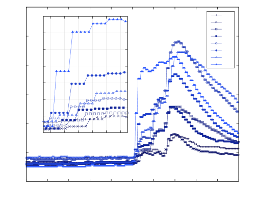
A batteryless sensor node can be composed of the modem module shown in Fig. 13 and a commercially available I2C-enabled sensor IC that operates as an I2C slave. A master device that initiates the I2C communication and collects sensor data, can be composed of the modem module and an MCU board. We used Teensy 3.2 and a temperature sensor IC, Microchip MCP9808 [40], as the master and the slaves, respectively. MCP9808 contains eight patterns of user-selectable I2C slave addresses. Therefore, eight sensors can operate on the same textile at the most. If the I2C slave address is fully programmable, the master can distinguish 112 slaves with the standard 7-bit I2C address except for 16 reserved addresses [23].
The entire system is the same as Fig. 5. A 3.3-V dc voltage was supplied to the bus via a 47-H RFC inductor. Further, 20-MHz and 50-MHz carriers were generated with a clock generator, Silicon Laboratories Si5351A [41]. The output clock signal is not a pure tone but a rectangular wave containing harmonics. To suppress the harmonics, the carries were supplied via LC series resonant circuits. Each of the pull-up impedances and is the series connection of the LC filter and a resistor. is a series connection of a 3.3H inductor, a 22-pF capacitor, and a 2.0-k resistor. is a series connection of a 3.3H, a 2.2-pF capacitor, and a 2.0-k resistor.
The master MCU board was connected to a PC with a universal serial bus (USB) cable, and the collected temperature data were visualized by a plotting software. Time-series temperature data captured when steam is sprayed onto the sensor array is plotted in Fig. 16.
Because the I2C slave addresses are preset, when the batteryless slaves are attached on the textile, they can immediately join the network, i.e., plug-and-play operation is achieved. We have included a supplementary MP4 video clip that demonstrates the plug-and-play operation of the sensor nodes. This will be available at http://ieeexplore.ieee.org.
VI Conclusion
We proposed the I2Wethat enables an I2C-formatted signal transfer along with a continuous dc power supply on a single transmission line. Double-sided conductive textiles can be used as the transmission line. I2We enables the simple implementation of a body sensor network, in which a number of batteryless and antennaless sensors are distributed over clothing. Individual wires connecting individual devices are eliminated. Each device was attached on the textile medium with a tack connector that allows for the physical mounting and electrical connection to be established using a single action.
The key component for the I2We implementation was the T-network filters that enabled the passive modulation of carriers with SCL and SDA signals. The passive modulation approach enabled the carrier generators to be separated from each device, and contributed to the smaller footprint and lower power consumption of each device. This paper described the design procedure and operation of the T-filters in detail. The reactance of each branch of the T-network was determined by considering the impedance poles and zeros.
I2C is the de facto standard of serial communication between sensor ICs and MCUs, and various sensor ICs equipped with the I2C interface are commercially available. Additionally, the software libraries of MCUs for I2C communication with sensor ICs can be used for I2We without any modification. Therefore, the proposed I2We is expected to be used widely for wearable sensor systems.
References
- [1] D. Marculescu, R. Marculescu, N. H. Zamora, P. Stanley-Marbell, P. K. Khosla, S. Park, S. Jayaraman, S. Jung, C. Lauterbach, W. Weber, T. Kirstein, D. Cottet, J. Grzyb, G. Troster, M. Jones, T. Martin, and Z. Nakad, “Electronic textiles: A platform for pervasive computing,” Proceedings of the IEEE, vol. 91, no. 12, pp. 1995–2018, Dec 2003.
- [2] Y. Khan, A. E. Ostfeld, C. M. Lochner, A. Pierre, and A. C. Arias, “Monitoring of vital signs with flexible and wearable medical devices,” Advanced Materials, vol. 28, no. 22, pp. 4373–4395, 2016. [Online]. Available: https://onlinelibrary.wiley.com/doi/abs/10.1002/adma.201504366
- [3] M. Georgi, C. Amma, and T. Schultz, “Recognizing hand and finger gestures with imu based motion and emg based muscle activity sensing.” in Proceedings of the International Conference on Bio-inspired Systems and Signal Processing (BIOSIGNALS-2015), 2015, pp. 99–108.
- [4] S. Egusa, Z. Wang, N. Chocat, Z. Ruff, A. Stolyarov, D. Shemuly, F. Sorin, P. Rakich, J. Joannopoulos, and Y. Fink, “Multimaterial piezoelectric fibres,” Nature materials, vol. 9, no. 8, p. 643, 2010.
- [5] Y. Tajitsu, “Piezoelectret sensor made from an electro-spun fluoropolymer and its use in a wristband for detecting heart-beat signals,” IEEE Transactions on Dielectrics and Electrical Insulation, vol. 22, no. 3, pp. 1355–1359, June 2015.
- [6] H. Zhang, X. Tao, T. Yu, and S. Wang, “Conductive knitted fabric as large-strain gauge under high temperature,” Sensors and Actuators A: Physical, vol. 126, no. 1, pp. 129 – 140, 2006. [Online]. Available: http://www.sciencedirect.com/science/article/pii/S0924424705005832
- [7] W. Chunya, L. Xiang, G. Enlai, J. Muqiang, X. Kailun, W. Qi, X. Zhiping, R. Tianling, and Z. Yingying, “Carbonized silk fabric for ultrastretchable, highly sensitive, and wearable strain sensors,” Advanced Materials, vol. 28, no. 31, pp. 6640–6648, 2016. [Online]. Available: https://onlinelibrary.wiley.com/doi/abs/10.1002/adma.201601572
- [8] L. Buechley and M. Eisenberg, “The LilyPad Arduino: Toward Wearable Engineering for Everyone,” IEEE Pervasive Computing, vol. 7, no. 2, pp. 12–15, April 2008.
- [9] Q. Li and X. M. Tao, “Three-dimensionally deformable, highly stretchable, permeable, durable and washable fabric circuit boards,” Proceedings of the Royal Society of London A: Mathematical, Physical and Engineering Sciences, vol. 470, no. 2171, 2014. [Online]. Available: http://rspa.royalsocietypublishing.org/content/470/2171/20140472
- [10] Y. Kim, H. Kim, and H. J. Yoo, “Electrical characterization of screen-printed circuits on the fabric,” IEEE Transactions on Advanced Packaging, vol. 33, no. 1, pp. 196–205, Feb 2010.
- [11] N. Matsuhisa, M. Kaltenbrunner, T. Yokota, H. Jinno, K. Kuribara, T. Sekitani, and T. Someya, “Printable elastic conductors with a high conductivity for electronic textile applications,” Nature Communications, vol. 6, p. 7461, 2015.
- [12] L. Buechley and M. Eisenberg, “Fabric PCBs, electronic sequins, and socket buttons: Techniques for e-textile craft,” Personal Ubiquitous Comput., vol. 13, no. 2, pp. 133–150, Feb. 2009. [Online]. Available: http://dx.doi.org/10.1007/s00779-007-0181-0
- [13] K. V. Laerhoven, N. Villar, and H.-W. Gellersen, “A layered approach to wearable textile networks,” IET Conference Proceedings, pp. 61–66(5), January 2003. [Online]. Available: http://digital-library.theiet.org/content/conferences/10.1049/ic\_20030148
- [14] E. Wade and H. Asada, “Conductive fabric garment for a cable-free body area network,” IEEE Pervasive Computing, vol. 6, no. 1, pp. 52–58, Jan 2007.
- [15] J. Akita, T. Shinmura, and M. Toda, “Flexible network infrastructure for wearable computing using conductive fabric and its evaluation,” in 26th IEEE International Conference on Distributed Computing Systems Workshops (ICDCSW’06). IEEE, 2006, p. 65.
- [16] H. Shinoda, Y. Makino, N. Yamahira, and H. Itai, “Surface sensor network using inductive signal transmission layer,” in Proceedings of the Fourth International Conference on Networked Sensing Systems, Braunschweig, Germany, June 2007, pp. 201–206.
- [17] Y. Tajima, A. Noda, and H. Shinoda, “Signal and power transfer to actuators distributed on conductive fabric sheet for wearable tactile display,” in Proceedings of AsiaHaptics 2016, Kashiwanoha, Japan, November 2016, pp. 163–169.
- [18] A. Noda and H. Shinoda, “Frequency-division-multiplexed signal and power transfer for wearable devices networked via conductive embroideries on a cloth,” in 2017 IEEE MTT-S International Microwave Symposium Proceedings, Hawaii, USA, June 2017, pp. 1–4, TUIF1–21.
- [19] Maxim Integrated. Application note 3808: What is an iButton device? [Online]. Available: https://pdfserv.maximintegrated.com/en/an/AN3808.pdf
- [20] Dallas Semiconductor. 1-Wire MicroLAN evaluation kit. [Online]. Available: https://datasheets.maximintegrated.com/en/ds/DS9091K.pdf
- [21] E. Wade and H. H. Asada, “Wearable dc powerline communication network using conductive fabrics,” in Robotics and Automation, 2004. Proceedings. ICRA ’04. 2004 IEEE International Conference on, vol. 4, April 2004, pp. 4085–4090 Vol.4.
- [22] E. R. Wade and H. H. Asada, “Design of a broadcasting modem for a dc plc scheme,” IEEE/ASME Transactions on Mechatronics, vol. 11, no. 5, pp. 533–540, Oct 2006.
- [23] NXP Semiconductors, “UM10204: I2C-bus specification and user manual, Rev. 6,” 2014. [Online]. Available: https://www.nxp.com/docs/en/user-guide/UM10204.pdf
- [24] H. C. Ferreira, H. M. Grove, O. Hooijen, and A. J. H. Vinck, “Power line communications: an overview,” in AFRICON, 1996., IEEE AFRICON 4th, vol. 2, Sep 1996, pp. 558–563 vol.2.
- [25] C.-H. Liu, E. Wade, and H. H. Asada, “Reduced-cable smart motors using dc power line communication,” in Proceedings 2001 ICRA. IEEE International Conference on Robotics and Automation (Cat. No.01CH37164), vol. 4, May 2001, pp. 3831–3838 vol.4.
- [26] P. V. Nikitin and K. V. S. Rao, “Theory and measurement of backscattering from rfid tags,” IEEE Antennas and Propagation Magazine, vol. 48, no. 6, pp. 212–218, Dec 2006.
- [27] D. Bharadia, K. R. Joshi, M. Kotaru, and S. Katti, “BackFi: High Throughput WiFi Backscatter,” in Proceedings of the 2015 ACM Conference on Special Interest Group on Data Communication (SIGCOMM ’15), London, UK, August 2015, pp. 283–296.
- [28] B. Kellogg, V. Talla, S. Gollakota, and J. R. Smith, “Passive Wi-Fi: Bringing Low Power to Wi-Fi Transmissions,” in Proceedings of the 13th USENIX Symposium on Networked Systems Design and Implementation (NSDI ’16), Santa Clara, CA, USA, March 2016, pp. 151–164.
- [29] P. Zhang, M. Rostami, P. Hu, and D. Ganesan, “Enabling practical backscatter communication for on-body sensors,” in Proceedings of the 2016 ACM Conference on Special Interest Group on Data Communication (SIGCOMM ’16). New York, NY, USA: ACM, 2016, pp. 370–383. [Online]. Available: http://doi.acm.org/10.1145/2934872.2934901
- [30] A. Noda and H. Shinoda, “I2C-enabled batteryless sensors on double-layered conductive fabric,” in Proceedings of the 2018 IEEE 15th International Conference on Wearable and Implantable Body Sensor Networks, Las Vegas, NV, USA, Mar. 2018, p. 1.
- [31] R. C. Webb, A. P. Bonifas, A. Behnaz, Y. Zhang, K. J. Yu, H. Cheng, M. Shi, Z. Bian, Z. Liu, Y.-S. Kim et al., “Ultrathin conformal devices for precise and continuous thermal characterization of human skin,” Nature materials, vol. 12, no. 10, p. 938, 2013.
- [32] E. Sardini, M. Serpelloni, and V. Pasqui, “Wireless wearable t-shirt for posture monitoring during rehabilitation exercises,” IEEE Transactions on Instrumentation and Measurement, vol. 64, no. 2, pp. 439–448, Feb 2015.
- [33] Microchip Technology, Tip #6 Data Slicer, 2009, ch. 4, pp. 4–7. [Online]. Available: http://ww1.microchip.com/downloads/en/DeviceDoc/01146B.pdf
- [34] PJRC.COM, LLC. Teensy USB Development Board. [Online]. Available: https://www.pjrc.com/store/teensy32.html
- [35] NXP Semiconductors. (2012) Kinetis K20: 72MHz Cortex-M4 up to 288KB Flash (64 pin) (REV 3). [Online]. Available: https://www.nxp.com/docs/en/data-sheet/K20P64M72SF1.pdf
- [36] R. M. Foster, “A reactance theorem,” The Bell System Technical Journal, vol. 3, no. 2, pp. 259–267, April 1924.
- [37] EPCOS AG. Inductors - LTspice. [Online]. Available: https://en.tdk.eu/tdk-en/523002/design-support/design-tools/inductors/model-libraries-for-smt-and-leaded-inductors/ltspice
- [38] Linear Technology. LT5534: 50MHz to 3GHz RF Power Detector with 60dB Dynamic Range Data Sheet. [Online]. Available: http://www.analog.com/media/en/technical-documentation/data-sheets/5534fc.pdf
- [39] Rohm Co., Ltd. (2016) Input Full Swing, Push-pull Output CMOS Comparators - BU5265HFV. [Online]. Available: https://www.rohm.com/datasheet/BU5265HFV/bu5265xxx-e
- [40] Microcip Technology Inc. MCP9808 0.5∘C Maximum Accuracy Digital Temperature Sensor. [Online]. Available: http://ww1.microchip.com/downloads/en/DeviceDoc/25095A.pdf
- [41] Silicon Laboratories. Si5351A/B/C-B I2C-Programmable Any-Frequency CMOS Clock Generator + VCXO Datasheet. [Online]. Available: https://www.silabs.com/documents/public/data-sheets/Si5351-B.pdf