Wide band gap phase change material tuned visible photonics
Light strongly interacts with structures that are of a similar scale to its wavelength; typically nanoscale features for light in the visible spectrum. However, the optical response of these nanostructures is usually fixed during the fabrication. Phase change materials offer a way to tune the properties of these structures in nanoseconds. Until now, phase change active photonics use materials that strongly absorb visible light, which limits their application in the visible spectrum. In contrast, Stibnite (Sb2S3) is an under-explored phase change material with a band gap that can be tuned in the visible spectrum from 2.0 to 1.7 eV. We deliberately couple this tuneable band gap to an optical resonator such that it responds dramatically in the visible spectrum to Sb2S3 reversible structural phase transitions. We show that this optical response can be triggered both optically and electrically. High-speed reprogrammable Sb2S3 based photonic devices, such as those reported here, are likely to have wide applications in future intelligent photonic systems, holographic displays, and micro-spectrometers.
Fundamentally three mechanisms that can be used to tune the optical properties of nanostructures: (1) employing controllable refractive indices materials as surroundings; (2) mechanically changing the nanostructure shape and size; and (3) changing the charge density and dielectric function of the plasmonic materials themselves. For example, the tuneable refractive index of liquid crystals (LCs) has been used to change the spectral response of metamaterialskossyrev2005electric ; liu2012optically ; cetin2013thermal . However, the small change in refractive index and the relatively slow switching speed, which is usually on a millisecond to microsecond scale, limit both the tuneability and modulation ratekhoo2008theory . The second approach relies on changing the separation distance, size, or geometry of plasmonic structures in the photonic resonatorzhu2010mechanically ; cataldi2014growing ; millyard2012stretch ; yamaguchi2013electrically ; khirallah2015nanoelectromechanical . The main problem with the second approach is mechanical stress, which tends to limit the switching endurance and the tuning speed. The third approach is achieved by varying the carrier density and dielectric function of the constituent plasmonic materials, such as metalsnovo2009electrochemical ; rotenberg2009tunable , semiconductorsjain2013doped and graphenegao2013excitation . However, the high intrinsic carriers density in metal and relatively weak plasmonic response in semiconductors result in a limited spectral response.
Phase change material (PCM) active photonics exploits refractive index switching materials. The prototypical phase change material, Ge2Sb2Te5, can be reversibly switched on a sub-nanosecond time scale billions of times, and once switched no energy is needed to maintain the switched stateloke2012breaking ; simpson2011interfacial ; waldecker2015time . This allows the photonics devices to be programmed to have a specific response. Ge2Sb2Te5 exhibits a substantial refractive index change when switched between different structural states. Indeed phase change switching in tellurium–based materials has been commercialised for optical and electrical data storage applicationswuttig2007phase . Ge2Sb2Te5 has also been used to demonstrate switchable reflective colour display devices that are based on thin film Fabry-Perot cavities and plasmonic nanograting deviceshosseini2014optoelectronic ; yoo2016multicolor ; dong2016wideband ; wuttig2017phase . However, using Ge2Sb2Te5 to tune visible photonics devices is non-ideal due to the high absorption at above band gap photon energies and the relatively small change in the real component of the refractive index, , at visible frequencies. The small together with using ultra-thin Ge2Sb2Te5 layers, which are necessary to minimise excessive absorption of the visible lighthosseini2014optoelectronic , further restrict the phase transition induced optical path length change. Netherless, the potential of Ge-Sb-Te active photonics is apparent in the infrared, where its absorption coefficient is low, and is largercao2016controlling ; mkhitaryan2017tunable ; michel2014reversible ; tittl2015switchable ; li2016reversible . A further advantage of PCMs is that they maintain their structural state and only require energy during the switching process, which is a clear advantage over liquid crystals and mechanically tuned photonic devices.
For tuneable visible photonics, phase change materials with a low optical absorption in the visible spectrum are superior to highly absorbing materials, such as Ge2Sb2Te5. The quality factor (Q-factor) of optical resonators is a measure of how much energy is lost from the optical cavity, and this determines the spectral purity. Clearly, the imaginary component of the refractive index of tellurium–based PCMs deems these materials unsuitable for high-Q narrow band-pass filters in the visible spectrum. Moreover, for new tuneable transmissive filters, the transmission should be greater than 80%Yun15 . To solve the absorption problem, new phase change materials with wider optical band gaps are required to tune photonic structures. Until now, however, there are no reports of wide band-gap phase change material tuned photonics.
Herein, we avoid using tellurides such as Ge2Sb2Te5 and propose an unconventional PCM, Sb2S3, which has a much larger band gap and concomitantly lower absorption. Generally, sulphides have a much wider band gap than selenides, and selenides have a larger band gap than tellurides. Although sulphides’ optical band gap is generally smaller than that of oxides, their higher refractive indices and low phonon frequencies make them attractive for applications that require high transmission from the visible to the mid-infraredeggleton2011chalcogenide . The overall objective of this work is to demonstrate that wide band gap phase change materials with a tuneable absorption edge are highly suitable for active visible photonics.
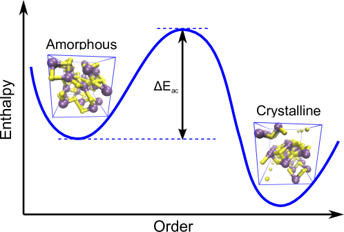
Stibnite (Sb2S3) is one of a number of chalcogenide PCMs that were studied in the 1990s for rewritable optical data storagearun1997effect . However, the Sb2S3 band gap is larger than the photon energy of the diode lasers that were used to read from and write to compact discs, which deemed Sb2S3 unsuitable for optical data storage devices. Here we show that Sb2S3 is misunderstood, and is well suited to both electrical and laser tuned active photonics. The reasons for this assertion are: (1) Sb2S3 is a wide band gap PCM that exhibits a large absorption edge shift at visible frequencies, (2) Sb2S3 exhibits a large in the visible spectrum during the structural phase transition, (3) Both the amorphous and crystalline phases of Sb2S3 are stable at room temperature, which is important for non-volatile programming of optical devices. (4) The phase transition temperatures of Sb2S3 are accessible by diode laser heating. (5) Sb2S3 has a crystallisation activation energy (Eac) of 2.0 eV (see Supplementary Information Figure S1), which is similar to that of Ge2Sb2Te5 (2.3 eV) Tominaga2009jjap .
Herein, we demonstrate that when Sb2S3 is used in resonator structures, it can easily be amorphised and reversibly switched on a nanosecond time scale between its amorphous and crystalline states. Indeed, we find that the low absorption and fast switching characteristics of Sb2S3 provide a substantial change to the resonant wavelength of reflective photonic devices in the visible spectrum. This is in stark contrast to the study in the 1990s that concluded Sb2S3 as a “write once and read many times” data-storage materialarun1999laser ; arun1997laser . Sb2S3 crystallises from an amorphous state into an orthorhombic structure at temperatures sufficient for its atoms to overcome the 2.0 eV energy barrier that separates the amorphous and crystalline statesbayliss1972refinement . This is depicted by the enthalpy–structural order diagram shown in Figure 1. The amorphous state is less stable than the crystalline structure, but the 2.0 eV activation energy barrier prevents it from spontaneously crystallising at room temperature. Crystallisation is achieved by heating Sb2S3 to temperatures higher than 573 K, whilst amorphisation involves heating above its 823 K melting temperatureMassalski90 and then rapidly quenching to ‘freeze-in’ the disordered amorphous state.
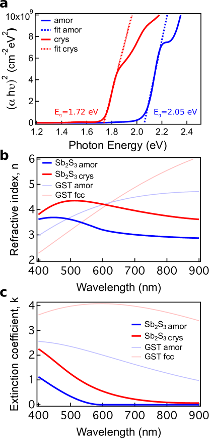
We find that Sb2S3 has very attractive properties for reprogrammable and tuneable visible photonics. The absorption edges of Sb2S3 in the amorphous and crystalline states are shown in Figure 2a. Amorphous Sb2S3 has a band gap of 2.05 0.05 eV, and crystalline Sb2S3 has a band gap of 1.72 0.05 eV. This corresponds to a 115 nm absorption edge red-shift upon crystallisation. In comparison to Sb2S3, Ge2Sb2Te5 has a band gap of 0.5 and 0.7 eV in the crystalline and amorphous stateslee2005investigation , which leads to strong absorption at visible frequencies. Ge2Sb2Te5 has a much higher extinction coefficient than Sb2S3 at visible frequencies, as shown in Figure 2c. The crystalline state of Sb2S3 has a higher refractive index than the amorphous state across the visible spectrum from 400 nm to 900 nm, as shown in Figure 2b. The maximum n 1 is at 614 nm, whilst the extinction coefficient is close to zero for the amorphous state at wavelengths greater than 605 nm, and for the crystalline state at wavelengths greater than 721 nm. This is important because a phase transition in Sb2S3 will change the absorption wavelength and also the concomitant condition for reflection and absorption of a thin film photonic resonator in the visible. In comparison to Ge2Sb2Te5, these characteristics of Sb2S3 imply that it is a more suitable phase change material for non-volatile tuneable visible photonics.
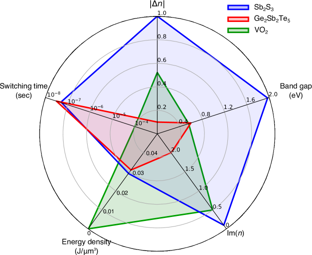
In summary, Sb2S3 shows a substantial change in refractive index, has a larger band gap and is far less absorbing than commonly used phase change materials, such as Ge2Sb2Te5 and VO2. We show later that the Sb2S3 crystallisation switching time is similar to the Ge2Sb2Te5 alloy, at 70 ns. The switching energy density of VO2 is lower than that of Sb2S3, however, VO2 requires a constant energy supply to hold its phase and optical properties. In contrast Sb2S3 exhibits a non-volatile change to its optical constants and only requires energy during the switching process. The radar chart that illustrates the superior properties of Sb2S3 relative to other tuneable media for active photonics devices in the visible spectrum is shown in Figure 3. The and Im(n) of Sb2S3, VO2 and Ge2Sb2Te5 are compared at a wavelength of 600 nm. A table that compares different tuning approaches to realise active photonic devices is shown in the Supplementary Information Table S1.
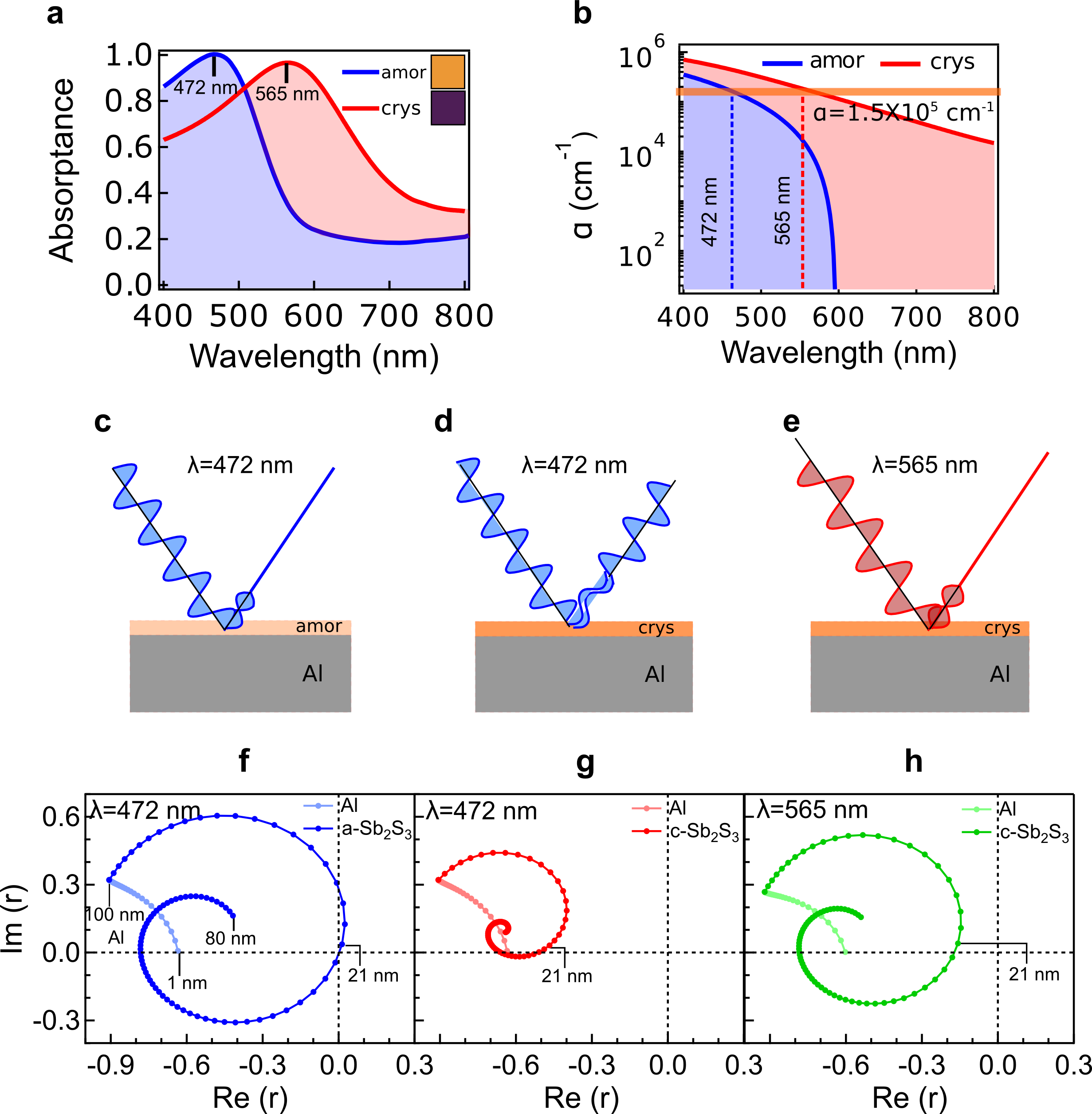
Here we show that actively tuning the damping coefficient of a critically damped PCM resonator by switching the Sb2S3 absorption edge results in a radical spectral response at visible frequencies. We start with a simple structure with 21 nm Sb2S3 on a 100 nm Al film. Perfect absorption of incident light is achieved by finely balancing the incident light reflected from the structure’s first interface with the absorption of light that is transmitted into the structure and then reflected out from buried interfaces. Figure 4a shows that this structure perfectly absorbs at a wavelength, nm. When Sb2S3 is crystallised, this absorptance maximum switches to nm. Perfect absorption in these structures occurs when the intrinsic absorption of the component layers reduces the light intensity reflected from buried interfaces to balance the light reflected from the top air-Sb2S3 interface. In addition, any optical phase changes that result from path length differences and interfacial reflections must also cancel. Thin sub-/4 absorbing semiconductor films form strong resonant behaviour at visible wavelengths due to a non- phase shift at the semiconductor–metal interfacekats2013nanometre . Here, this effect can cause destructive interference in the Sb2S3 films despite their thickness being an order of magnitude thinner than the wavelength of light.
The necessary balance of absorption and reflection is clear in Figure 4b. It shows the absorption coefficient of amorphous and crystalline Sb2S3 as a function of wavelength. The absorption coefficient was calculated from the extinction coefficient shown in Figure 2c. We see that the amorphous and crystalline absorptance maxima occur at wavelengths of 472 nm and 565 nm, where the absorption coefficient of Sb2S3 is 1.5105 cm-1. In effect, the wavelength for perfect absorption must increase across the absorption edge in order to balance the light reflected from the top air-Sb2S3 interface. Despite the difference between the real component at =472 nm and =565 nm being =0.3, the PCM film is just 21 nm thick, and the change in optical path length between the amorphous and crystalline states is minimal. The significant red-shift to the Sb2S3 absorption-edge in the visible spectrum, which is seen in Figure 2c and Figure 4b, dominates the interference condition.
A further way to see the effect of the edge shift is to plot the complex reflection coefficient, , as a function of the Sb2S3 film thickness at the absorptance maximum wavelengths, =472 nm and =565 nm. Figures 4f-h show how the reflection coefficient for an Al/Sb2S3 structure changes as the structure’s thickness increases. Initially, the Al and Sb2S3 are not present, and the reflection coefficient only has a real component, =-0.6, which gives rise to the 36% reflectivity of the silicon substrate. As the aluminium thickness increases, the reflection coefficient turns away from the real axis due to a small amount of absorption. Once the Al is 100 nm thick, the Sb2S3 layer is added and its thickness increases. As can be seen in Figure 4b, Sb2S3 has an absorption coefficient of 1.5105 for the amorphous and crystalline states at nm and nm respectively, hence the imaginary component of the reflection coefficient, Im(r), is large. When its thickness is 21 nm, and the total structure thickness is 121 nm, the reflectance coefficient is =, and the material is perfectly absorbing at =472 nm. Further increasing the Sb2S3 thickness increases the net loss of the system, and the reflected intensity from the top air-Sb2S3 interface is no longer suppressed. Hence the reflectance coefficient moves away from the origin. For comparison, similar plots for Ge2Sb2Te5, which is highly absorbing in the visible, are given in Supplementary Figure S2.
Crystallising the Sb2S3 increases the loss and therefore produces a much smaller spiral radius in the complex plane at =472 nm, as shown in Figure 4g. It is now impossible at this wavelength to produce perfect absorption by simply increasing the Sb2S3 thickness. However, increasing the incident wavelength to =565 nm decreases the absorption, and the radius of the complex plane spiral increases such that the reflectance coefficient of a 21 nm thick Sb2S3 film is close to 0, see Figure 4h. Indeed, we observe a peak in the absorptance spectrum in Figure 4a. Note that for Ge2Sb2Te5 films, the perfect absorption peaks occur in the infrared and are not present in the visible spectrum unless additional dispersive elements are added to the structure dong2016wideband . We conclude that the imaginary component of the Sb2S3 refractive index, Im(n), predominately drives the change in absorptance maximum. Thus, this design mainly exploits the change in Im(n) rather than Re(n), which is usually used to tune Ge2Sb2Te5 deviceswuttig2017phase ; tittl2015switchable ; li2016reversible .
To further show the effect of using the Sb2S3 absorption edge change to tune at visible wavelength, an Al/Si3N4/Sb2S3/Si3N4/Al stacked structure was designed. This simple device structure was deliberately chosen to demonstrate the superior performance of Sb2S3, rather than a new type of photonics device. The bottom and top Al thicknesses were 100 nm and 3 nm, respectively. The device structure is schematically shown in Figure 5a. Si3N4 diffusion barriers was also included between the Al and Sb2S3 layers to prevent inter-layer diffusion, which is known to be a problem when metals interface directly with phase change chalcogenideschew2017chalcogenide . The top Al layer was included because it increases the Q-factor of the resonator and also allows the PCM to be electrically addressed, see Figure 5b and Supplementary Figure S3. The thickness of the Sb2S3 layer is varied from 11 nm to 67 nm to shift the absorptance maximum wavelength.
The reflectance spectra of the Al/Si3N4/Sb2S3/Si3N4/Al structures were measured and simulated, see Supplementary Figure S4. Effectively, Sb2S3 switches from a low-loss to lossy dielectric as the wavelength is scanned from the near-infrared to the short-visible. The Sb2S3 structural phase transition red-shifts the resonator’s natural frequency, and this causes the strong reflected colour change, which is clearly seen in the photographs of the sample that are displayed in Figure 5c and Supplementary Figure S5. Figures 5d-5e show the photographs and corresponding reflectance spectra for the sample in the amorphous and crystalline states when the thickness of Sb2S3 is 24 nm. For the 24 nm thick Sb2S3 structure shown in Figure 5e the absorptance peak is red-shifted by 110 nm from 520 nm to 630 nm. We also see in Supplementary Figure S4 that as the thickness of the Sb2S3 layer increases, the peak absorptance wavelength is red-shifted across the visible spectrum from 425 nm to 710 nm. The corresponding simulations reproduce the key spectral features that are observed in the measurement.
The red-shift to the spectra shown in Figures 5e is directly due to the intrinsic absorption edge of Sb2S3 narrowing from 2.0 eV to 1.7 eV. The metal–Sb2S3–metal structure is designed to resonate at wavelengths close to this absorption-edge, which amplifies the effect of the absorption edge switching on- and off- the resonant wavelength, thus producing the large change in reflected colour. However, crystalline Sb2S3 is slightly more absorbing than the amorphous state, and this causes a broader resonance, as shown in Figure 5e and Supplementary Figures S4–S5.
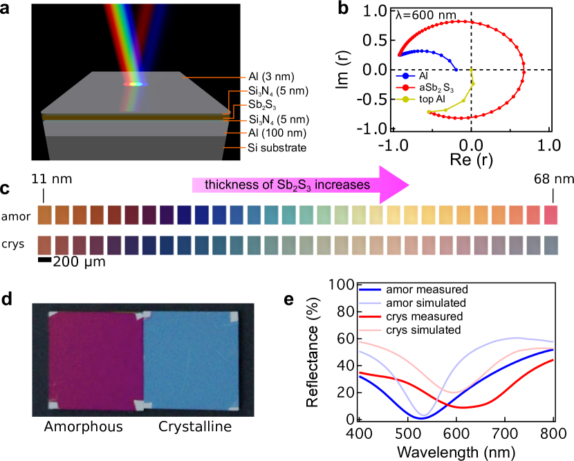
Achieving a large colour shift from a 24 nm thick Sb2S3 film may seem surprising considering the change in the 0.9 produces a 32 nm optical path length change at 550 nm. This corresponds to a phase shift of =0.36 rad, which has a negligible effect on the reflected colour. However, for this metal-Sb2S3 structure, the colour change is dominated by the Sb2S3 absorption edge red-shift effect on the imaginary component of the refractive index, which at =550 nm changes from 0.08 to 0.83, see Figure 2c.
Active photonics devices must be tuneable or capable of switching between different states. Here we demonstrate both reversible laser switching and electrical switching. The dichotomy for well-studied phase change materials along the GeTe-Sb2Te3 tie-line is that they are stable at room temperature but quickly and efficiently undergo a structural phase transition at slightly elevated temperatureswuttig2007phase . This is also a characteristic of Sb2S3. Here we show that Sb2S3 can also be crystallised and amorphised at a similar speed to Ge2Sb2Te5. A pump-probe nanosecond laser system was used to simultaneously heat the Sb2S3 film and measure the change in reflectivity of the heated samplebehera2017laser . Figure 6a shows the normalised reflectivity as a function of time for the crystallisation of Sb2S3 in the Al(100 nm)/Si3N4(5 nm)/Sb2S3(19 nm)/Si3N4(5 nm)/Al(3 nm) structure. The amorphous film completely crystallises in 78 4 ns. These pump laser amorphised marks have a diameter of 1.5 m. Therefore, we rastered a 5 ns, =532 nm amorphising laser pulse over a 0.25 area to make the amorphous region visible. A photograph of the amorphised area is shown in Figure 6b. The initial amorphous colour was pink and after crystallisation the colour changed to blue. We can clearly see that after rastering the amorphising laser, the structure’s colour is switched reversibly back from the crystallised state to the amorphous state. Figure 6c shows the corresponding reflectance spectra from the structure with Sb2S3 in the as-deposited amorphous state, crystallised state, and the re-amorphised state. A video showing the recrystallisation process is included in the Supplementary Information. Note that the reamorphised state’s spectra and colour are marginally less reflective, and this is due to ablation at the centre of the laser’s Gaussian intensity profile. We conclude that Sb2S3 can be reamorphised in 5 ns to produce large reversible changes to the visible spectrum. This is important because until now, it has been claimed that Sb2S3 is a “write once, read many times” materialarun1999laser ; arun1997laser , and the optical change is insignificant. However, by designing the resonant wavelength of Sb2S3-metal structures to coincide with the absorption edge of Sb2S3, strong interference effects can be exploited to efficiently absorb the 532 nm light in Sb2S3 layers that are just 21 nm thick, which in turn allows amorphisation. We have included further data for amorphisation of other metal–Sb2S3 structures in Supplementary section 4.
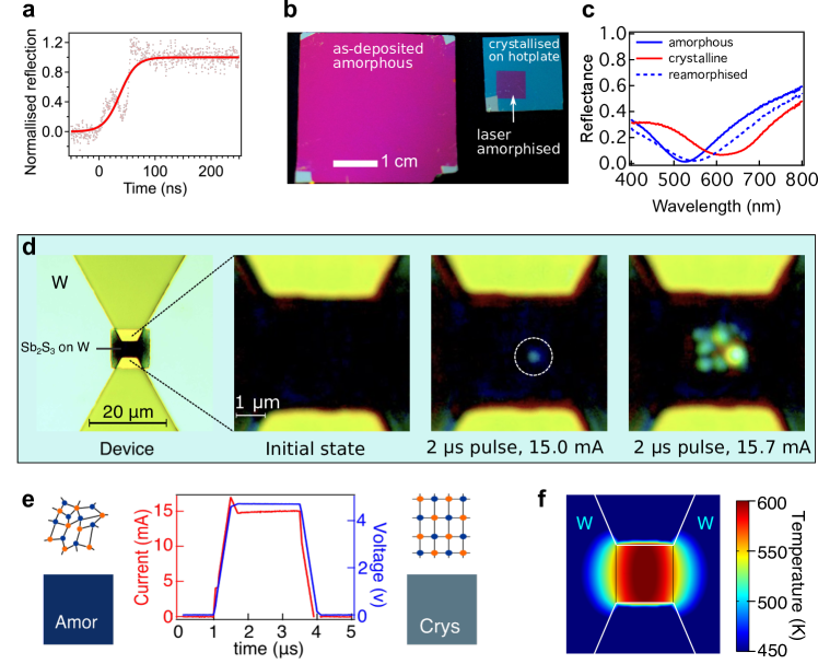
Many active photonics devices are electrically addressed, and therefore we show that these metal/Sb2S3 filters can be electrically switched. We adopted a line-cell design similar to those proposed for reconfigurable GHz switcheschamplain2016examination but without the RF waveguide. The Sb2S3 was deposited directly on top of a tungsten filament. This configuration allows direct optical probing of the active Sb2S3 area before and after applying electrical pulses. The electric current through the W filament causes Joule heating. The heat is conducted into the Sb2S3 layer, which provides the energy for it to undergo a phase transition between the amorphous and crystalline structural states. Figure 6d shows images of the device in the initial state before applying an electrical pulse, after applying a 2 s, 15.0 1 mA pulse, and finally after applying a 2 s, 15.7 1 mA pulse. We designed the structure to be highly absorbing in the visible spectrum when Sb2S3 is amorphous, and consequently the image of the active area is dark. The simulated colour for the W/Sb2S3 structure in the amorphous and crystalline states is inset into Figure 6e, whilst the spectra is shown in Supplementary Information Fig. S7. The crystallised region should become a light blue-grey colour. Applying the electrical pulse heats the amorphous structure, allowing it to crystallise at temperatures higher than 585 K. An electrical Joule heating finite element simulation shows the temperature distribution in the Sb2S3 film after applying a 2 s, 15 mA pulse, see Figure 6f. This results in crystallisation at the hottest part of the active area, which according to the Joule heating finite element simulation temperature distribution, is the central area of the Sb2S3 where the temperature is higher than the crystallisation temperature. Indeed, Figure 6d illustrates that the 2 s, 15 mA pulse produces a light blue-grey crystalline mark at the centre area of the device. This indicates that Sb2S3 is readily switched using the electrical Joule heating device. The crystallised area can be increased by adjusting the electrical pulses applied to heat the device and optimising its thermal design. However, this particular device design is susceptible to small increases in the electrical current, which causes ablation of the hottest area in the sample. This is seen in Figure 6d when a 15.7 mA, 2 s pulse is applied to the sample.
In conclusion, the wide band gap phase change materials Sb2S3 has excellent properties for visible photonics and is therefore preferred over more conventional PCMs, such as Ge2Sb2Te5, which was originally developed for data storage applications. The bandgap of Sb2S3 is large and produces an absorption edge which can be shifted in the visible spectrum in nanosecond time scales by structural phase transitions. In contrast to exploiting a change in the real part of the PCMs refractive index, which is usually used to tune Ge2Sb2Te5 infrared photonic resonators, we show that the Sb2S3 band gap tuneability can be used to tune resonant photonics devices, thus producing a substantial change to the spectral response and resultant colour. The fast switching, large optical band gap, and tuneable refractive index deem Sb2S3 a versatile phase change material for tuneable photonics at visible frequencies. Considering the lack of reported large band-gap phase change materials and the emergence of smart photonics, where flexibility and programmability of components and materials are required, wide band gap phase change materials, such as Sb2S3, will lead to a broad range of innovative photonic devices.
Experimental Section
Fabrication
Aluminium films were deposited on Si(001) substrates by DC sputtering, and Si3N4 and Sb2S3 were deposited by radio frequency (RF) sputtering.
The chamber base pressure was 410-5 Pa and the sputtering pressure was 0.5 Pa.
The deposition rate was 0.5 Å/min from an Sb2S3 alloy target with a diameter of 50.8 mm and a purity of 99.9 %.
Si3N4 was deposited by using a gas mixture of Ar: N2=8:2 from a Si target.
To crystallise the Sb2S3 in the optical filter, the samples were heated at 300 ∘C for 30 minutes on a hot plate.
Optical band gap measurement
The optical band gaps were calculated by Tauc analysestauc1968optical .
As Sb2S3 has a direct energy band gap, the - was used, where is absorption coefficient, is photon energy, is band gapjellison1996parameterization .
Ellipsometry
The optical constants of Sb2S3 in the amorphous and crystalline states were measured using an ellipsometry spectrometer (WVASE, J.A Woollam Co.).
37 nm of as-deposited Sb2S3 deposited on Si (001) substrate was used for measurement.
A further sample with the same thickness was crystallised in a tube furnace at 300 ∘C in an argon atmosphere for 20 minutes.
A heating rate of 4 K/min was used.
Both samples were measured by ellipsometry.
The wavelength range of incident light is from 250 nm to 900 nm and the angle of incident light was 65.1∘.
The data was fitted by Lorentz and Tauc-Lorentz oscillator models for both amorphous and crystalline states.
The fit parameters are listed in the Supplementary Information table S2, whilst the spectroscopic ellipsometric parameters and the computed refractive indices are available at www.actalab.com.
Reflectance spectra
Reflectance spectra of the Al/Si3N4/Sb2S3/Si3N4/Al structures were measured using a QDI 2010 UV-visible-NIR range microspectrophotometer (CRAIC Technology Inc., California, USA).
The reflectance spectra were normalised to an Al mirror, which was considered 100% reflective across the measured spectral range.
The absorptance maximum wavelengths were obtained by Gaussian fitting at the dip of the reflectance spectra.
Laser switching
A pump-probe system with pulse length from 20 ns to 2000 ns and pulse power up to 40 mW was used to switch the Al/Sb2S3/Al structurebehera2017laser .
A 658 nm pump laser with higher power was used to induce a phase transition in the Sb2S3 film.
To measure the change in reflected signal, a 100 W and 1 s probe laser was used.
A 635 nm probe laser was used to focus the probe beam on the write mark.
The reflected probe signal was detected simultaneously by the fast silicon photodetectors.
The final data was measured by a digitising oscilloscope (NI PXIe-5162, 10 bit, 1.5 GHz).
A camera was used to image the sample surface.
We assumed that the crystallised fraction was directly proportional to the change in the probe light.
Optical microscope images
To compare the colours of the optical filters with different Sb2S3 thickness, the bright field optical micro images of the colour filter were taken using an Olympus BX51 microscope through a 10 objective lens.
Each colour square is 680 m 680 m.
Acknowledgement
This research was performed under the auspices of the SUTD-MIT International Design Center (IDC). The research project was funded by the Samsung GRO, the A-star Singapore-China joint research program Grant No. 1420200046, and the SUTD Digital Manufacturing and Design Centre (DManD) Grant No. RGDM 1530302. We are grateful for fruitful discussions with Seokho Yun.
References
- (1) P. A. Kossyrev, A. Yin, S. G. Cloutier, D. A. Cardimona, D. Huang, P. M. Alsing, J. M. Xu. Nano Lett. 2005, 5, 10 1978.
- (2) Y. Liu, G. Si, E. Leong, B. Wang, A. Danner, X. Yuan, J. Teng. Appl. Phys. A 2012, 107, 1 49.
- (3) A. E. Cetin, A. Mertiri, M. Huang, S. Erramilli, H. Altug. Adv. Opt. Mater. 2013, 1, 12 915.
- (4) I.-C. Khoo, J.-H. Park, J. D. Liou. JOSA B 2008, 25, 11 1931.
- (5) X. Zhu, L. Shi, X. Liu, J. Zi, Z. Wang. Nano Res. 2010, 3, 11 807.
- (6) U. Cataldi, R. Caputo, Y. Kurylyak, G. Klein, M. Chekini, C. Umeton, T. Bürgi. J. Mater. Chem. C 2014, 2, 37 7927.
- (7) M. G. Millyard, F. Min Huang, R. White, E. Spigone, J. Kivioja, J. J. Baumberg. Appl. Phys. Lett. 2012, 100, 7 073101.
- (8) K. Yamaguchi, M. Fujii, T. Okamoto, M. Haraguchi. Appl. Phys Express 2013, 7, 1 012201.
- (9) K. Khirallah, M. A. Swillam. Journal of Micro/Nanolithography, MEMS, and MOEMS 2015, 14, 2 025501.
- (10) C. Novo, A. M. Funston, A. K. Gooding, P. Mulvaney. J. Am. Chem. Soc. 2009, 131, 41 14664.
- (11) N. Rotenberg, J. N. Caspers, H. M. van Driel. Phys. Rev. B 2009, 80, 24 245420.
- (12) P. K. Jain, K. Manthiram, J. H. Engel, S. L. White, J. A. Faucheaux, A. P. Alivisatos. Angew. Chem. 2013, 125, 51 13916.
- (13) W. Gao, G. Shi, Z. Jin, J. Shu, Q. Zhang, R. Vajtai, P. M. Ajayan, J. Kono, Q. Xu. Nano Lett. 2013, 13, 8 3698.
- (14) D. Loke, T. Lee, W. Wang, L. Shi, R. Zhao, Y. Yeo, T. Chong, S. Elliott. Science 2012, 336, 6088 1566.
- (15) R. Simpson, P. Fons, A. Kolobov, T. Fukaya, M. Krbal, T. Yagi, J. Tominaga. Nat. Nanotechnol. 2011, 6, 8 501.
- (16) L. Waldecker, T. A. Miller, M. Rudé, R. Bertoni, J. Osmond, V. Pruneri, R. E. Simpson, R. Ernstorfer, S. Wall. Nat. Mater. 2015, 14, 10 991.
- (17) M. Wuttig, N. Yamada. Nat. Mater. 2007, 6, 11 824.
- (18) P. Hosseini, C. D. Wright, H. Bhaskaran. Nature 2014, 511, 7508 206.
- (19) S. Yoo, T. Gwon, T. Eom, S. Kim, C. S. Hwang. ACS Photonics 2016, 3, 7 1265.
- (20) W. Dong, Y. Qiu, J. Yang, R. E. Simpson, T. Cao. J. Phys. Chem. C 2016, 120, 23 12713.
- (21) M. Wuttig, H. Bhaskaran, T. Taubner. Nat. Photonics 2017, 11, 8 465.
- (22) T. Cao, J. Bao, L. Mao, T. Zhang, A. Novitsky, M. Nieto-Vesperinas, C.-W. Qiu. ACS Photonics 2016, 3, 10 1934.
- (23) V. K. Mkhitaryan, D. S. Ghosh, M. Rudé, J. Canet-Ferrer, R. A. Maniyara, K. K. Gopalan, V. Pruneri. Adv. Opt. Mater. 2017, 5, 1.
- (24) A.-K. U. Michel, P. Zalden, D. N. Chigrin, M. Wuttig, A. M. Lindenberg, T. Taubner. ACS Photonics 2014, 1, 9 833.
- (25) A. Tittl, A.-K. U. Michel, M. Schäferling, X. Yin, B. Gholipour, L. Cui, M. Wuttig, T. Taubner, F. Neubrech, H. Giessen. Adv. Mater. 2015, 27, 31 4597.
- (26) P. Li, X. Yang, T. W. Maß, J. Hanss, M. Lewin, A.-K. U. Michel, M. Wuttig, T. Taubner. Nat. Mater. 2016, 15, 8 870.
- (27) S. Yun. Personal communtication, 2015.
- (28) B. J. Eggleton, B. Luther-Davies, K. Richardson. Nat. Photonics 2011, 5, 3 141.
- (29) P. Arun, A. Vedeshwar. J. Non-Cryst. Solids 1997, 220, 1 63.
- (30) J. Tominaga, T. Shima, P. Fons, R. Simpson, M. Kuwahara, A. Kolobov. Jpn. J. Appl. Phys 2009, 48, 3 03A053.
- (31) P. Arun, A. Vedeshwar, N. Mehra. J. Phys. D: Appl. Phys. 1999, 32, 3 183.
- (32) P. Arun, A. Vedeshwar, N. Mehra. Mater. Res. Bull. 1997, 32, 7 907.
- (33) P. Bayliss, W. Nowacki. Zeitschrift für Kristallographie-Crystalline Materials 1972, 135, 1-6 308.
- (34) T. Massalski, H. Okamoto, P. Subramanian, L. Kacprzak. Binary Alloy Phase Diagrams, 2nd Edition. ASM International, 1990.
- (35) B.-S. Lee, J. R. Abelson, S. G. Bishop, D.-H. Kang, B.-k. Cheong, K.-B. Kim. J. Appl. Phys. 2005, 97, 9 093509.
- (36) M. A. Kats, R. Blanchard, P. Genevet, F. Capasso. Nat. Mater. 2013, 12, 1 20.
- (37) L. T. Chew, W. Dong, L. Liu, X. Zhou, J. Behera, H. Liu, K. V. Sreekanth, L. Mao, T. Cao, J. Yang, et al. In Active Photonic Platforms IX, volume 10345. International Society for Optics and Photonics, 2017 103451B.
- (38) J. K. Behera, X. Zhou, J. Tominaga, R. E. Simpson. Opt. Mater. Express 2017, 7, 10 3741.
- (39) J. G. Champlain, L. B. Ruppalt, A. C. Guyette, N. El-Hinnawy, P. Borodulin, E. Jones, R. M. Young, D. Nichols. J. Appl. Phys. 2016, 119, 24 244501.
- (40) J. Tauc. Mater. Res. Bull. 1968, 3, 1 37.
- (41) G. Jellison Jr, F. Modine. Appl. Phys. Lett. 1996, 69, 3 371.