Graphene: Free electron scattering within an inverted honeycomb lattice
Abstract
Theoretical progress in graphene physics has largely relied on the application of a simple nearest-neighbor tight-binding model capable of predicting many of the electronic properties of this material. However, important features that include electron-hole asymmetry and the detailed electronic bands of basic graphene nanostructures (e.g., nanoribbons with different edge terminations) are beyond the capability of such simple model. Here we show that a similarly simple plane-wave solution for the one-electron states of an atom-based two-dimensional potential landscape, defined by a single fitting parameter (the scattering potential), performs better than the standard tight-binding model, and levels to density-functional theory in correctly reproducing the detailed band structure of a variety of graphene nanostructures. In particular, our approach identifies the three hierarchies of nonmetallic armchair nanoribbons, as well as the doubly-degenerate flat bands of free-standing zigzag nanoribbons with their energy splitting produced by symmetry breaking. The present simple plane-wave approach holds great potential for gaining insight into the electronic states and the electro-optical properties of graphene nanostructures and other two-dimensional materials with intact or gapped Dirac-like dispersions.
The two-dimensional (2D) honeycomb carbon-atom lattice known as graphene Geim and Novoselov (2007) is a promising material for applications in optical and electronic devices Liu et al. (2011); Vicarelli et al. (2012); Schwierz (2010). In particular, its peculiar conical electronic dispersion Semenoff (1984); Castro Neto et al. (2009) and 2D character enable a uniquely large optical tunability Fei et al. (2012); Chen et al. (2012) and a suitable playground for quantum electrodynamics phenomena, such as the relativistic Klein tunneling Katselson et al. (2006), as well as a customizable zoo of exotic band structures when decorated with defects Forsythe et al. (2018), arranged in twisted bilayers Cao et al. (2018), or laterally patterned into ribbons Fujita et al. (1996); Nakada et al. (1996). Energy-gap engineering in graphene, an essential prerequisite for nanoelectronics applications, demands controlled and selective sub-lattice perturbations at the atomic scale, such as chemical doping Joucken et al. (2015); Gierz et al. (2008) or gating Peres (2010), lateral strain Ni et al. (2008); Conrad et al. (2017), and substrate-induced sublattice asymmetry Zhou et al. (2007); Vita et al. (2014); Papagno et al. (2012); Varykhalov et al. (2012).
Graphene nanoribbons (GNRs) have been extensively studied as simple, appealing nanostructures that lead to electronic band features, such as gap opening, due to quantum confinement, and peculiar edge states that can readily be tuned through their width, shape, and edge-terminations Fujita et al. (1996); Nakada et al. (1996). The rapidly progressing on-surface chemistry, which allows controlled-synthesis of novel graphene-based nanostructures, such as GNRs with complex architectures Chen et al. (2015); Di Giovannantonio et al. (2018); Bronner et al. (2018); Gröning et al. (2018); Rizzo et al. (2018); Moreno et al. (2018), combined with the precise mapping of their electronic structures using angle-resolved photomission spectroscopy (ARPES) and scanning tunneling spectroscopy (STS) Ruffieux et al. (2012); Senkovskiy et al. (2018a); Carbonell-Sanromá et al. (2018); Magda et al. (2014), make GNRs promising candidates for the realization of exotic graphene-based nanodevices Ihn et al. (2010); Llinas et al. (2017); Celis et al. (2016).
Theoretical understanding and prediction of extended graphene and GNRs properties has been instrumental in the development of the field. Density-functional theory (DFT) accurately describes their electronic structures, but simpler methods are preferred because they allow us to gain further physical insight. In particular, following the pioneering work of Wallace Wallace (1947), the tight-binding (TB) model has played a central role in the theoretical description of the electronic structure of extended graphene, yielding remarkable agreement with DFT calculations. However, noticeable discrepancies between TB and DFT show up when describing GNRs with either armchair (AGNR) or zigzag (ZGNR) edge terminations. For example, the widely used nearest-neighbors TB predicts two families of AGNRs, namely semiconductor and metallic, depending on the number of carbon-dimer lines along the ribbon width () Nakada et al. (1996), while three semiconductor categories are obtained from DFT calculations Son et al. (2006a) in agreement with STS experiments Kimouche et al. (2015); Merino-Díez et al. (2017); Söde et al. (2015); Li et al. (2014).
Both nearest-neighbors TB and nearly-free electron (NFE) models are well-known textbook approaches for band-structure calculations in solids Kittel (1987); Ashcroft and Mermin (1976). Within the NFE framework, plane wave expansions (PWEs) of the electron states have traditionally played an important role, for example in the description of electron scattering in metallic and molecular superlattices Mugarza et al. (2001); Ortega and García de Abajo (2007); Piquero-Zulaica et al. (2017). In particular, 2D hexagonal superlattices, which are known to exhibit graphene-like band structures with -point gap and symmetry-protected degeneracy at the -points Malterre et al. (2011); Abd El-Fattah et al. (2011), are well described by the PWE approach. Unfortunately, such simple PWEs have not been used for the description of extended graphene or GNRs, although a close correspondence between the TB and NFE models was demonstrated for the so-called graphene, in which the Shockley surface state confined by a hexagonal CO superlattice was shown to exhibit a Dirac-like dispersion Gomes et al. (2012).
Here, we demonstrate that the electronic characteristics of atomic graphene could be finely reproduced via a simple NFE model with a single fitting parameter, namely the scattering potential. In this context, the graphene non-Bravais honeycomb lattice is alternatively modeled as a 2D hexagonal lattice made of the 6-fold symmetric, hexagonally-warped inner part of the carbon rings, where a sufficiently large repulsive potential () is assigned [Fig. 1 (a)]. The potential barrier in reality delimits the attractive Coulomb potential of each carbon atom ( and ). Perfect agreement with DFT calculations is obtained for the band structure, local density of states (LDOSs), and constant energy surfaces (CESs) using an Electron-Plane-Wave-Expansion (EPWE) implementation (see Methods). Interestingly, with the same single fitting parameter , the model captures the three categories of AGNRs in decent agreement with DFT. Likewise, the 1D-bulk band structure and the nearly-degenerate edge state for ZGNRs are obtained in agreement with TB and DFT without any assistance of electron-electron interactions. Additionally, we find that when the symmetry of the two carbon sublattices is broken for ZGNRs (), which is a common situation for graphene grown onto different substrates, the edge state of ZGNRs is split in energy, here without the incorporation of electron-electron interactions. We believe that this simplified picture can be efficiently applied to explore different varieties of atomic graphene-like extended and finite structures.
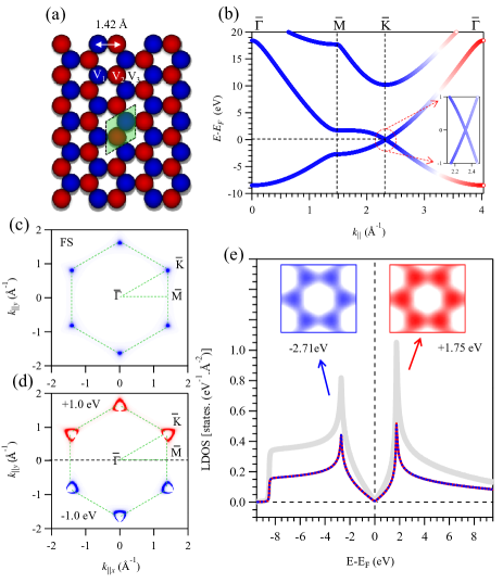
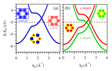
Figure 1 summarizes the electronic characteristics of free-standing graphene, as determined within the EPWE approach. The potential landscape used in the calculation is depicted in Fig. 1(a). The red and blue circles define the position of the carbon atoms, each of radius , and the white regions stand for the carbon-free voids. The unit cell, enclosing one void and two carbon atoms, is marked by the black lines (shaded area), with unit-cell vectors of length . The band structure presented in Fig. 1(b) is obtained by setting the potential difference between the voids ( = 23 eV) and the two equivalent carbon atoms ( = = 0) to V = 23 eV and the effective mass ( ) to unity. These parameters, which coincide with the binding energy of the carbon 2 level car (2000) and the free electron mass (), nicely reproduce the band structure of free-standing graphene obtained from DFT calculations and experiments Puschnig and Lüftner (2015); Rybkina et al. (2013). The Fermi energy () is set at the non-gapped (see zoom-in) Dirac point, and the -point energy is accordingly found at -8.5 eV. The lower and upper edges of the -point gap are -2.71 eV and +1.75 eV, respectively, while the slope of the linear bands at the points is eV [i.e., Fermi velocity () 1 106 m/s], in perfect agreement with literature values Dedkov and Voloshina (2015). We stress that small deviations from the employed value of and yield noticeable changes on the relative energetic position of the bands, the size of the -point gap, and the degree of electron-hole asymmetry [see Supplementary Information (SI), Fig. S1).
In Fig 1(c-d) we present the simulated photoemission intensity of the constant energy surfaces (CESs). The Fermi surface (FS) consists of single spots centered at the six -points of the Brillouin zone (BZ, green lines), resulting from intact Dirac cones [Fig. 1(c)]. At lower and higher binding energies ( +1 eV and -1 eV), these spots diverge into the characteristic graphene triangular pockets, as shown, respectively, in the upper (red) and lower (blue) panels of Fig. 1(d). The trigonal shape of these CESs further reassures that the electron-hole asymmetry present in (b), which in TB calculations is accounted for by employing additional hopping parameters for second/third nearest neighbors / Castro Neto et al. (2009); Kretinin et al. (2013); Reich et al. (2002), is naturally captured by EPWE. Indeed, the different hopping parameters employed in TB are consistent with the different effective potentials ( height width) felt by electrons moving from one carbon towards neighboring atoms. Furthermore, the variation of the photoemission intensity within the trigonal pockets agrees nicely with recent ARPES experiments Fedorov et al. (2014); Ulstrup et al. (2018); Varykhalov et al. (2008); Vita et al. (2014). The electronic characteristics of graphene, as deduced from the total-DOS (TDOS) and LDOS, are also presented in Fig. 1(e). The V-like peculiarities at are revealed in the TDOS per unit cell (gray) and the LDOS at the two carbon atoms (blue and red), all exhibiting clear electron-hole asymmetry. The onsets of LDOS at -8.5 eV define the -point energy, whereas the peaks at -2.71 eV and +1.75 eV are the borders of the -point gap. The LDOS at the two carbon atoms are clearly coincident, a common finding for pristine graphene. The 2D LDOS maps depicted at the insets and taken at the boundaries of the -point gap are identical, confirming the absence of -point gaps based on symmetry considerations Malterre et al. (2011); Abd El-Fattah et al. (2011). Given the calculations and analysis presented in Fig. 1, the electronic features of a free-standing graphene sheet obtained from experiments and DFT calculations are well-reproduced.

Perturbations induced by a graphene support (i.e., a substrate, and/or the deposition of adsorbates/dopants) have shown to change the electronic properties of graphene in different ways. Figure 2 presents possible electronic modifications in one of such perturbation cases, as calculated using the present EPWE model. In Fig. 2(a), we explore the effect of broken symmetry for the two carbon atoms on the electronic structure. The band structure is obtained by assigning different potentials for each carbon-sublattice ((red) = -1 eV and (blue) = +1 eV). The main modification is the opening of an energy gap at the point (g() = 1.3 eV), which is a natural consequence of the broken symmetry of the potential landscape within the unit cell. Such broken-symmetry-induced gaps have been reported experimentally for different graphene systems, such as graphene grown on Ir(111) Kralj et al. (2011), Ru(0001) Brugger et al. (2009), hydrogenated-graphene Balog et al. (2010), and other systems Zhou et al. (2007); Vita et al. (2014); Papagno et al. (2012); Varykhalov et al. (2012, 2008). The large symmetry-induced gap shown here is meant only to highlight the effect, but the actual values of and can be tuned to yield the experimental gap. We also note that the -point energy is unaltered in this particular example, as the average of the potentials and is zero, and is only shifted in energy otherwise. The TDOS and LDOS spectra presented in (b) precisely follow these band structure modifications. In addition to the peaks at the borders of the -point gap, a deviation from the V-shape peculiarities occurs for all spectra where, instead, the TDOS and LDOS vanish at the energy range spanning the -point gap boundaries. Particularly relevant is the non-equivalence of the LDOS at the two carbon atoms within the unit cell, where the weight of the LDOS changes from one carbon (red) to the second sublattice (blue) by crossing the energy gap, which is further shown in the 2D LDOS presented in Fig. 2(b, right). Additional electronic modifications, such as hybridization and doping, which still preserve the -point degeneracy, are briefly presented in SI, Fig. S2.
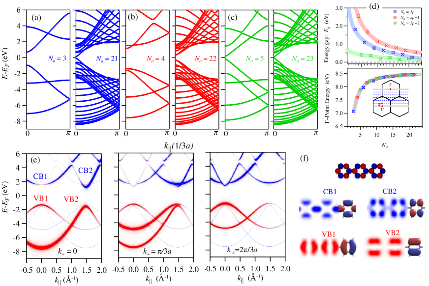
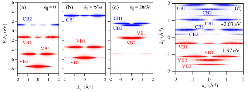
The calculations/analysis here presented clearly reveal that the electronic structure of graphene could be reproduced by simple geometrical regions in which specific values of the potential are assigned. In what follows, we explore the applicability of this approach to the study of both AGNRs and ZGNRs. We employ the same geometry and potential landscape while varying the ribbon width and termination. We assume that the ribbons are infinitely extended along the ribbon axis ( i.e., the -direction), and decoupled in -direction by separating them by 20 Å gaps. Figure 3 (a-c) depicts the band structure along the ribbon axis for the three different classes of AGNRs with (a) = 3, (b) = 3+1 , and (c) = 3+2 , where is a positive integer [here, = 1 (left) and 7 (right)]. In contrast to standard TB calculations, the three types exhibit energy gaps () with (3+1) (3) (3+2), and their width follows an inverse proportionality (see colored curves in (d)) in agreement with DFT calculations. Notice that the carbon-carbon distance in the bulk region and at the ribbon boundaries is fixed here to the same value (i.e., structural relaxation is not considered, although DFT indicates a 3.5% contraction in the bond length at the edges) Son et al. (2006a), yet the model yields appreciable energy gaps for the 3+2 family. We also show that the -point energy, irrespectively of the ribbon family, asymptotically approaches -point of extended graphene by increasing the width, strictly following the width-dependent point energy (gray curve) obtained by stepping along the Brillouin zone slices of graphene (see inset to (d)). Particularly relevant is the shallow dispersion of the bands at -2.6 eV for the = 3 (a) and = 5 (c), which in standard TB exhibit no dispersion Vasseur et al. (2016); Nakada et al. (1996). This, further, indicates that the NFE approach naturally considers all possible crosstalk/hopping between neighboring carbon atoms with the scattering potential as a single fitting parameter.
In what follows, we check the capability of our model to simulate the photoemission intensity and density of states for nanoribbons. This should serve as a guidance for experimentalists to perform proper assignments of specific GNR bands, which might become problematic for wider ribbons with nearby dispersing bands, and in general, due to strong variations in intensity caused by effects related to the photoemission matrix element. Figure 3(e) presents the simulated photoemission intensity for the 4-AGNR along the ribbon axis. A subtle variation of photoemission intensity for different bands is clear. For example, at = 0 (left), the frontier valence band (VB1) has predominantly-symmetric spectral weight around = 0, while VB2 gains spectral weight over wider range with asymmetric photoemission intensity around the top of the band ( 1.5 Å-1). This distribution of photoemission intensity changes drastically at different , such as = /3 (center) and 2/3 (right). Indeed, these are all 1D bands, and therefore, are not dispersing in the perpendicular direction (), yet strong photoemission intensity modulation is present for the VB and CB alike [SI, Fig. S3(a)]. Therefore, constant-energy surfaces (i.e., vs maps) such as the one shown in the SI, Fig. S3(b), are essential for a proper assignment of bands. Actually, the simulation of such photoemission intensity maps has recently solved a long-standing contradiction between STS and ARPES data for the 7-AGNR, where the VB2 was mistakenly assigned in ARPES experiments to the VB1 Senkovskiy et al. (2018a); foo . A further confirmation of the full functionality of our model is provided by comparing the calculated 2D-LDOS to the molecular orbitals obtained from DFT calculations, and in particular, for the 3-AGNR, as shown in Fig. 3 (f). The matching between LDOS (left) and DFT orbitals (right) is remarkable Piquero-Zulaica et al. (unpublished). The overall agreement with DFT extends even beyond the description of simple AGNRs: complex graphene-based structures such as zigzag Piquero-Zulaica et al. (unpublished) and heterogeneous ribbons, as well as nanoporous graphene Moreno et al. (2018), are equally well described using our NFE approach (see SI, Fig. S4).
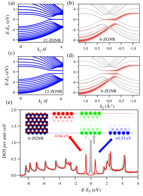
Likewise, the electronic structure of ZGNRs could be obtained using our EPWE approach. Figure 4(a-b) presents band structure calculations for selected ZGNRs with = 12 (a) and 6 (b). Their characteristic bulk bands and the energy-degenerate edge states are obtained in agreement with TB and DFT calculations when on-site Hubbard potentials and exchange interactions, respectively, are not considered. In (b) the simulated photoemission intensity for the 6-ZGNR is also shown at = 0, with the edge state exhibiting a high-enough spectral weight as to be probed by average techniques such as ARPES, provided that ZGNRs aligned on substrates are experimentally available on large areas.
As previously discussed, for an extended graphene sheet with symmetry-broken carbon sublattices, a -point gap opens up (see Fig. 2). Here we demonstrate the effect that this broken symmetry has on the electronic structure of ZGNRs, specifically on the edge state. By assigning different values to the potentials at the two carbons sublattices ( = -1 eV and = +1 eV), taking the 12-ZGNR as an example, we show that the edge state is split in energy, while the 1D-bulk projected bands are practically unaltered [Fig. 4(c)]. The energy gap between the split edge states is the same as the size of the -point gap of the corresponding extended graphene presented in Fig. 2(a). Both bands of the energy-split edge state have reasonable photoemission spectral weights, as demonstrated for the 6-ZGNR at = 0 in (d). Finally, we present in Fig. 4(e) the DOS curves for the free-standing (gray) and symmetry-broken (red) sublattices in the 6-ZGNR, where an energy-splitting of the DOS peak at is obtained. Although the DOS profile for asymmetric ribbons (red) resembles the one reported experimentally (and from DFT) for the 6-ZGNR Ruffieux et al. (2016), the broken-symmetry-induced gaps could be distinguished from electron-electron-interaction gaps Son et al. (2006a, b); Yang et al. (2008) by plotting the 2D spatial distribution of the LDOS taken at the energy of the edge state, as shown on top of the spectra in Fig. 4(e). The insets present the EPWE geometry of the 6-ZGNR and the 2D-LDOS taken at the energy of the lower (red) and upper (blue) edge states, where the LDOS is clearly localized at one edge, while for fully symmetric ribbons both edges are equally occupied at (green). Notice that the one-edge localization of the LDOS has not experimentally been reported, neither for degenerate nor for energy-split edges states, yet its realization could have potential impact as a switch in 1D conduction-channels through gating. We also anticipate that the combination of broken symmetry and electron correlation should produce a clear imbalance in the LDOS at both edges of the ribbons, in addition to the intrinsic asymmetry produced by the different dispersion of the upper and lower edges of the gap and the electron-hole asymmetry.
The fact that the extended and finite graphene characteristics are well captured within the framework of the NFE model could have far reaching implications, since some of the electronic structure variations and size dependence are not unique to graphene. Similar atomic systems, such as silicene or boron nitrides, could be understood following the same approach. Furthermore, nanometer-sized ribbons made from hexagonal superlattices, such as molecular graphene Gomes et al. (2012) or metallic superlattices possessing graphene-like band structures Malterre et al. (2011), should exhibit these types of size dependence variations. What makes these variations experimentally accessible and potentially relevant for technology in the graphene case, and in other 2D atomic lattices, is the combination of a large -point gap (several eV), which for superlattices reduces to just a few meV, and the steep dispersion near the points. Finally, this simple NFE description of graphene and its nanostructures should have large impact on the efficient simulation of graphene-based devices and phenomena, such as negative refraction and super lenses in - junctions, using, for example, the complementary electronic boundary-element method (EBEM) solver, which was previously used to describe similar effects in 2D metallic superlattices García de Abajo et al. (2010); Abd El-Fattah et al. (2017).
In conclusion, we have showed that the electronic structure of the band in free-standing and perturbed graphene can be well described by a simple nearly-free-electron model (EPWE) applied to an inverted honeycomb lattice defined by a sufficiently large confining potential. With the same single fitting parameter (i.e., the scattering barrier) the electronic properties of graphene nanostructures, such as armchair and zigzag GNRs, are well described. Our approach simplifies the exploration of newly emerging artificial systems with fundamental and technological interest, such as nanostructured 2D materials, topological GNR junctions with peculiar end states Gröning et al. (2018); Rizzo et al. (2018), and artificial flat band lattices Leykam et al. (2018).
Acknowledgements.
This work has been supported in part by the Spanish MINECO (Grant Nos. MAT2014-59096-P, MAT-2016-78293-C6, MAT-2017-88374-P, MAT2017-88492-R, and SEV2015-0522), the Basque Government (Grant No. IT-621-13), the Catalan CERCA Program, Fundació Privada Cellex, and AGAUR (Grant No. 2017 SGR 1651).METHODS
Effective 2D potential description. We simulate the electronic structure of graphene in terms of the one-electron states of a 2D potential landscape, in which each carbon atom is represented by a circle filled with uniform potential, embedded in a flat interstitial region (see Fig. 1(a)). We then write the Schrödinger equation as
| (1) |
where the energy is expressed relative to a reference level (e.g., the Dirac point), is the effective mass, is the 2D potential as a function of spatial coordinates along the graphene plane, and is the electron wave function.
Plave-wave expansion for periodic systems. We take to be periodic and express it in terms of Fourier components as
| (2) |
where the sum extends over 2D reciprocal lattice vectors with coefficients calculated as an integral over the first Brillouin zone (1BZ), normalized to the unit-cell area . Using Bloch’s theorem, we anticipate electron wave functions labeled by a band index and the 2D wave vector within the 1BZ:
| (3) |
where we use the (infinite) number of cells for normalization purposes. Inserting Eqs. (2) and (3) into Eq. (1), we find the linear system of equations
| (4) | |||
Because is a Hermitian matrix with indices and , for each value of we obtain different bands of real eigenenergies and eigenstates of coefficients . We solve Eq. (4) by retaining a finite number of ’s within a sufficiently large distance to the origin in reciprocal space. The eigenstates form an orthonormal system,
provided we impose the normalization condition .
LDOS calculation for periodic systems. The local density of states (LDOS) is directly calculated from its definition
In practice, we use the prescription and evaluate this integral in a dense grid by interpolating the eigenstates and eigenenergies within each grid element.
Calculation of photoemission angular distributions for periodic systems. For simplicity, we dismiss the contribution of the normal component of the electron wave function to the photoemission matrix elements, as it should just introduce a smooth and broad angular dependence, which we represent through a multiplicative coefficient in the resulting photoemission intensity. We focus instead on the contribution of the in-plane wave function and further approximate the parallel component of the photoelectron wave function as a normalized plane wave . The angle-resolved photoemission intensity corresponding to a binding energy and photoelectron wave vector is then given from Fermi’s golden rule as
where in the last expression is chosen such that lies within the 1BZ.
I SUPPLEMENTARY INFORMATION
I.1 Electron-hole asymmetry
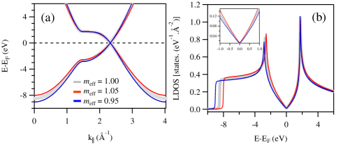
The inherent electron-hole asymmetry of graphene manifests itself as slightly different band dispersions above and below the Dirac-point, and consequently, a clear deviation from a symmetric V-shape is clearly observable in the LDOS, as shown in Fig. 1. This asymmetry shows up in conventional DFT calculations and in experiments, while the popular nearest-neighbors TB model requires additional hopping parameters to account for it Kretinin et al. (2013). In contrast, our NFE approach captures electron-hole asymmetry, which can be tuned to fit experimental data through a small adjustment in the effective mass. Figure S1 presents the band structures (a) and DOS per unit cell (b) for = (10.05) compared with = (in gray). We note the strong modifications of the electronic band structure (about 500 meV variation in the -point energy) with slight (5) relaxation of . The inset to (b) highlights the electron-hole asymmetry near the Dirac point Andrei et al. (2012).
I.2 Graphene-substrate hybridization and doped graphene
It is a well-established result for graphene, or generally for 2D materials with lattice, that the degeneracy at the points is protected by both structural and time-reversal symmetries. However, for some graphene/substrate combinations, such as graphene on Co(0001), the symmetry of the carbon sublattices is broken while the Dirac cone remains intact. To explain this effect, a dynamical hybridization scenario has been discussed Varykhalov et al. (2012). Such systems can also be modeled within our approach. From a simple NFE model argument, the size of the -point gap (and the -point gap as well, if allowed by symmetry considerations) scales with the scattering potential. The latter is actually proportional to the product of the barrier height () and width. By setting the covalent radii of the carbon atoms to 0.63 Å (red) and 0.71 Å (blue), we can close the -point gap, although the symmetry of the voids is reduced to three-fold, as shown in Fig. S2(a). In fact, the 2D LDOS map at the lower and upper edges of the -point gap are exactly the same as in free-standing graphene [see Fig. 1(e)], where the LDOS associated with the two carbon atoms are identical. Therefore, it is difficult to distinguish free-standing and asymmetric non-gapped graphene based on LDOS data, such as provided by STS experiments. However, the -point energy is shifted towards lower binding energy as a result of the increased area of the voids at the expense of the covalent radii of the carbon atoms. For larger radii, where an overlap between the carbon atoms occurs, the -point shifts instead toward higher binding energy. We note that the closing of the -point gap in the symmetry-broken graphene of Fig. S2(a) is always associated with or doping. This conditional doping can be used in experiments to distinguish asymmetric non-gapped from pristine graphene. We also note that the doping here differs from conventional - or -doping of pristine graphene, in which there is no breaking of the symmetry of the carbon atoms, thus leading to a rigid downward/upward energy shift , as shown in Fig. S2(b). Here, the band structures for -doped (green) and -doped (red) graphene are obtained by setting = = -1 eV and = = +1 eV, respectively.
I.3 Photoemission intensity
In Fig. S3(a-c) we show the photoemission intensity of the 1D bands (i.e., perpendicular to the ribbon axis) for the 4-AGNR. All bands exhibit a strong intensity modulation, so that specific bands light up at selective values of . For example, CB2 and CB1 have spectral weight for = 0 (a) and = /3 (b), respectively, while both VB1 and VB2 exhibit peaks at = /3 (c). The vs maps taken at 2.03 eV (top) and -1.95 eV (bottom) are presented in (d), allowing us to obtain a proper band assignment from ARPES measurements, which have been routinely simulated in recent works Senkovskiy et al. (2018a); Piquero-Zulaica et al. (unpublished); Senkovskiy et al. (2018b).
I.4 Heterogeneous AGNR and nanoporous graphene (NPG)
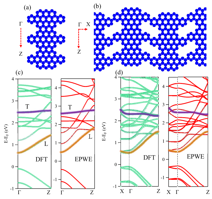
In this section, we demonstrate the ability of our NFE approach to describe the electronic structure of more complex graphene-based nanostructures. We take the 7-13-AGNR structure Moreno et al. (2018), which has a modulation in width between 7 and 13 carbon atoms, as an example for heterogeneous nanoribbons and junctions [Fig. S4(a)]. We also consider nanoporous graphene (NPG) Moreno et al. (2018) made from the connections between these self-assembled 7-13-AGNR in an out-of-phase configuration [Fig. S4(b)]. In the potential landscapes shown in (a-b), the blue circles define the carbon atoms with ==0, while the void and pore potentials are set to =23 eV. The band structures obtained from our EPWE approach [Fig. S4(c-d), right] are compared with the ones obtained from DFT [Fig. S4(c-d), left] Moreno et al. (2018). Our model clearly captures the essential features of the DFT band structures, including the gap size, as well as the L and T states.
References
- Geim and Novoselov (2007) A. K. Geim and K. S. Novoselov, Nat. Mater. 6, 183 (2007).
- Liu et al. (2011) M. Liu, X. Yin, E. Ulin-Avila, B. Geng, T. Zentgraf, L. Ju, F. Wang, and X. Zhang, Nature 474, 64 (2011).
- Vicarelli et al. (2012) L. Vicarelli, M. S. Vitiello, D. Coquillat, A. Lombardo, A. C. Ferrari, W. Knap, M. Polini, V. Pellegrini, and A. Tredicucci, Nat. Mater. 11, 4176 (2012).
- Schwierz (2010) F. Schwierz, Nat. Nanotech. 5, 487 (2010).
- Semenoff (1984) G. W. Semenoff, Phys. Rev. Lett. 53, 2449 (1984).
- Castro Neto et al. (2009) A. H. Castro Neto, F. Guinea, N. M. R. Peres, K. S. Novoselov, and A. K. Geim, Rev. Mod. Phys. 81, 109 (2009).
- Fei et al. (2012) Z. Fei, A. S. Rodin, G. O. Andreev, W. Bao, A. S. McLeod, M. Wagner, L. M. Zhang, Z. Zhao, M. Thiemens, G. Dominguez, et al., Nature 487, 82 (2012).
- Chen et al. (2012) J. Chen, M. Badioli, P. Alonso-González, S. Thongrattanasiri, F. Huth, J. Osmond, M. Spasenović, A. Centeno, A. Pesquera, P. Godignon, et al., Nature 487, 77 (2012).
- Katselson et al. (2006) M. I. Katselson, K. S. Novoselov, and A. K. Geim, Nat. Phys. 2, 620 (2006).
- Forsythe et al. (2018) C. Forsythe, X. Zhou, K. Watanabe, T. Taniguchi, A. Pasupathy, P. Moon, M. Koshino, P. Kim, and C. R. Dean, Nat. Nanotech. 13, 566 (2018).
- Cao et al. (2018) Y. Cao, V. Fatemi, S. Fang, K. Watanabe, T. Taniguchi, E. Kaxiras, and P. Jarillo-Herrero, Nature 556, 43 (2018).
- Fujita et al. (1996) M. Fujita, K. Wakabayashi, K. Nakada, and K. Kusakabe, J. Phys. Soc. Jpn. 65, 1920 (1996).
- Nakada et al. (1996) K. Nakada, M. Fujita, G. Dresselhaus, and M. S. Dresselhaus, Phys. Rev. B 54, 17954 (1996).
- Joucken et al. (2015) F. Joucken, Y. Tison, P. L. Fèvre, A. Tejeda, A. Taleb-Ibrahimi, V. R. E. Conrad, C. Chacon, A. Bellec, Y. Girard, S. Rousset, et al., Sci. Rep. 5, 14564 (2015).
- Gierz et al. (2008) I. Gierz, C. Riedl, U. Starke, C. R. Ast, and K. Kern, Nano Lett. 8, 4603 (2008).
- Peres (2010) N. M. R. Peres, Rev. Mod. Phys. 82, 2673 (2010).
- Ni et al. (2008) Z. H. Ni, T. Yu, Y. H. Lu, Y. Y. Wang, Y. P. Feng, and Z. X. Shen, ACS Nano 2, 2301 (2008).
- Conrad et al. (2017) M. Conrad, F. Wang, M. Nevius, K. Jinkins, A. Celis, M. Narayanan Nair, A. Taleb-Ibrahimi, A. Tejeda, Y. Garreau, A. Vlad, et al., Nano Lett. 17, 341 (2017).
- Zhou et al. (2007) S. Y. Zhou, G. H. Gweon, A. V. Fedorov, P. N. First, W. A. de Heer, D. H. Lee, F. Guinea, A. H. Castro Neto, and A. Lanzara, Nat. Mater. 6, 3288 (2007).
- Vita et al. (2014) H. Vita, S. Böttcher, K. Horn, E. N. Voloshina, R. E. Ovcharenko, T. Kampen, A. Thissen, and Y. S. Dedkov, Sci. Rep. 4, 5704 (2014).
- Papagno et al. (2012) M. Papagno, S. Rusponi, P. M. Sheverdyaeva, S. Vlaic, M. Etzkorn, D. Pacilé, P. Moras, C. Carbone, and H. Brune, ACS Nano 6, 199 (2012).
- Varykhalov et al. (2012) A. Varykhalov, D. Marchenko, J. Sánchez-Barriga, M. R. Scholz, B. Verberck, T. O. W. B. Trauzettel, C. Carbone, , and O. Rader, Phys. Rev. X 2, 041017 (2012).
- Chen et al. (2015) Y.-C. Chen, T. Cao, C. Chen, Z. Pedramrazi, D. Haberer, D. G. de Oteyza, F. R. Fischer, S. G. Louie, and M. F. Crommie, Nat. Nanotech. 10, 156 (2015).
- Di Giovannantonio et al. (2018) M. Di Giovannantonio, O. Deniz, J. I. Urgel, R. Widmer, T. Dienel, S. Stolz, C. Sánchez-Sánchez, M. Muntwiler, T. Dumslaff, R. Berger, et al., ACS Nano 12, 74 (2018).
- Bronner et al. (2018) C. Bronner, R. A. Durr, D. J. Rizzo, Y.-L. Lee, T. Marangoni, A. M. Kalayjian, H. Rodriguez, W. Zhao, S. G. Louie, F. R. Fischer, et al., ACS Nano 12, 2193 (2018).
- Gröning et al. (2018) O. Gröning, X. Y. Sh. Wang, C. A. Pignedoli, G. B. Barin, C. Daniels, A. Cupo, V. Meunier, X. Feng, A. Narita, K. Müllen, et al., Nature 560, 209 (2018).
- Rizzo et al. (2018) D. J. Rizzo, G. Veber, T. Cao, C. Bronner, T. Chen, F. Zhao, H. Rodriguez, S. G. Louie, M. F. Crommie, and F. R. Fischer, Nature 560, 204 (2018).
- Moreno et al. (2018) C. Moreno, M. Vilas-Varela, B. Kretz, A. Garcia-Lekue, M. V. Costache, M. Paradinas, M. Panighel, G. Ceballos, S. O. Valenzuela, D. Peña, et al., Science 360, 199 (2018).
- Ruffieux et al. (2012) P. Ruffieux, J. Cai, N. C. Plumb, L. Patthey, D. Prezzi, A. Ferretti, E. Molinari, X. Feng, K. Müllen, C. A. Pignedoli, et al., ACS Nano 6, 6930 (2012).
- Senkovskiy et al. (2018a) B. V. Senkovskiy, D. Y. Usachov, A. V. Fedorov, D. Haberer, N. Ehlen, F. R. Fischer, and A. Grüneis, 2D Mater. 5, 035007 (2018a).
- Carbonell-Sanromá et al. (2018) E. Carbonell-Sanromá, A. Garcia-Lekue, M. Corso, G. Vasseur, P. Brandimarte, J. Lobo-Checa, D. G. de Oteyza, J. Li, S. Kawai, S. Saito, et al., J. Phys. Chem. C 122, 16092 (2018).
- Magda et al. (2014) G. Z. Magda, X. Jin, I. Hagymási, P. Vancsó, Z. Osváth, P. Nemes-Incze, C. Hwang, L. P. Biró, and L. Tapasztó, Nature 514, 608 (2014).
- Ihn et al. (2010) T. Ihn, J. Güttinger, F. Molitor, S. Schnez, E. Schurtenberger, A. Jacobsen, S. Hellmüller, T. Frey, S. Dröscher, C. Stampfer, et al., Mater. Today 13, 44 (2010).
- Llinas et al. (2017) J. P. Llinas, A. Fairbrother, G. Borin Barin, W. Shi, K. Lee, S. Wu, B. Y. Choi, R. Braganza, J. Lear, N. Kau, et al., Nat. Commun. 8, 633 (2017).
- Celis et al. (2016) A. Celis, M. N. Nair, A. Taleb-Ibrahimi, E. H. Conrad, C. Berger, W. A. de Heer, and A. Tejeda, J. Phys. D: Appl. Phys. 49, 143001 (2016).
- Wallace (1947) P. R. Wallace, Phys. Rev. 71, 622 (1947).
- Son et al. (2006a) Y.-W. Son, M. L. Cohen, and S. G. Louie, Nature 444, 348 (2006a).
- Kimouche et al. (2015) A. Kimouche, M. M. Ervasti, R. Drost, S. Halonen, A. Harju, P. M. Joensuu, J. Sainio, and P. Liljeroth, Nat. Commun. 6, 10177 (2015).
- Merino-Díez et al. (2017) N. Merino-Díez, A. Garcia-Lekue, E. Carbonell-Sanromá, J. Li, M. Corso, L. Colazzo, F. Sedona, D. Sánchez-Portal, J. I. Pascual, and D. G. de Oteyza, ACS Nano 11, 11661 (2017).
- Söde et al. (2015) H. Söde, L. Talirz, O. Gröning, C. A. Pignedoli, R. Berger, X. Feng, K. Müllen, R. Fasel, and P. Ruffieux, Phys. Rev. B 91, 045429 (2015).
- Li et al. (2014) Y. Li, M. Chen, M. Weinert, and L. Li, Nat. Commun. 5, 4311 (2014).
- Kittel (1987) C. Kittel, Quantum theory of solids (Wiley, New York, 1987).
- Ashcroft and Mermin (1976) N. W. Ashcroft and N. D. Mermin, Solid State Physics (Harcourt College Publishers, Philadelphia, 1976).
- Mugarza et al. (2001) A. Mugarza, A. Mascaraque, V. Pérez-Dieste, V. Repain, S. Rousset, F. J. García de Abajo, and J. E. Ortega, Phys. Rev. Lett. 87, 107601 (2001).
- Ortega and García de Abajo (2007) J. E. Ortega and F. J. García de Abajo, Nat. Nanotech. 2, 601 (2007).
- Piquero-Zulaica et al. (2017) I. Piquero-Zulaica, J. Lobo-Checa, A. Sadeghi, Z. M. Abd El-Fattah, C. Mitsui, T. Okamoto, R. Pawlak, T. Meier, A. Arnau, J. E. Ortega, et al., Nat. Commun. 8, 787 (2017).
- Malterre et al. (2011) D. Malterre, B. Kierren, Y. Fagot-Revurat, C. Didiot, F. J. García de Abajo, F. Schiller, J. Cordón, and J. E. Ortega, New J. Phys. 13, 013026 (2011).
- Abd El-Fattah et al. (2011) Z. M. Abd El-Fattah, M. Matena, M. Corso, F. J. García de Abajo, F. Schiller, and J. E. Ortega, Phys. Rev. Lett. 107, 066803 (2011).
- Gomes et al. (2012) K. K. Gomes, W. Mar, W. Ko, F. Guinea, and H. C. Manoharan, Nature 483, 306 (2012).
- car (2000) NIST X-ray Photoelectron Spectroscopy Database, NIST Standard Reference Database Number 20 (National Institute of Standards and Technology, 2000).
- Puschnig and Lüftner (2015) P. Puschnig and D. Lüftner, J. Electr. Spectrosc. Relat. Phenom. 200, 193 (2015).
- Rybkina et al. (2013) A. A. Rybkina, A. G. Rybkin, A. V. Fedorov, D. Y. Usachov, M. E. Yachmenev, D. E. Marchenko, O. Y. Vilkov, A. V. Nelyubov, V. K. Adamchuk, and A. M. Shikin, Surf. Sci. 609, 7 (2013).
- Dedkov and Voloshina (2015) Y. Dedkov and E. Voloshina, J. Phys.: Condens. Matter 27, 303002 (2015).
- Kretinin et al. (2013) A. Kretinin, G. L. Yu, R. Jalil, Y. Cao, F. Withers, A. Mishchenko, M. I. Katsnelson, K. S. Novoselov, A. K. Geim, and F. Guinea, Phys. Rev. B 88, 165427 (2013).
- Reich et al. (2002) S. Reich, J. Maultzsch, C. Thomsen, and P. Ordejón, Phys. Rev. B 66, 035412 (2002).
- Fedorov et al. (2014) A. V. Fedorov, N. I. Verbitskiy, D. Haberer, C. Struzzi, L. Petaccia, D. Usachov, O. Y. Vilkov, D. V. Vyalikh, J. Fink, M. Knupfer, et al., Nat. Commun. 5, 3257 (2014).
- Ulstrup et al. (2018) S. Ulstrup, P. Lacovig, F. Orlando, D. Lizzit, L. Bignardi, M. Dalmiglio, M. Bianchi, F. Mazzola, A. Baraldi, R. Larciprete, et al., Surf. Sci. (2018), URL https://doi.org/10.1016/j.susc.2018.03.017.
- Varykhalov et al. (2008) A. Varykhalov, J. Sánchez-Barriga, A. M. Shikin, C. Biswas, E. Vescovo, A. Rybkin, D. Marchenko, and O. Rader, Phys. Rev. Lett. 101, 157601 (2008).
- Kralj et al. (2011) M. Kralj, I. Pletikosić, M. Petrović, P. Pervan, M. Milun, A. T. N’Diaye, C. Busse, T. Michely, J. Fujii, and I. Vobornik, Phys. Rev. B 84, 075427 (2011).
- Brugger et al. (2009) T. Brugger, S. Günther, B. Wang, J. H. Dil, M.-L. Bocquet, J. Osterwalder, J. Wintterlin, and T. Greber, Phys. Rev. B 79, 045407 (2009).
- Balog et al. (2010) R. Balog, B. Jørgensen, L. Nilsson, M. Andersen, E. Rienks, M. Bianchi, M. Fanetti, E. Lagsgaard, A. Baraldi, S. Lizzit, et al., Nat. Mater. 9, 315 (2010).
- Vasseur et al. (2016) G. Vasseur, Y. Fagot-Revurat, M. Sicot, B. Kierren, L. Moreau, D. Malterre, L. Cardenas, G. Galeotti, J. Lipton-Duffin, F. Rosei, et al., Nat. Commun. 7, 10235 (2016).
- (63) Vicinal surfaces are frequently used for ARPES measurement, because they help to align graphene nanoribbons and define the direction. However, the nanoribbon plane could be tilted a few degrees with respect to the vicinal surface plane, leading to an uncertain normal emission geometry, and hence to a sizeable projection. For example, using a vicinal surface and He I excitation energy (=21.2 eV), could vary by as much as 0.2 Å-1, where ( stands for the work function), leading to a confusing assignment of the detected nanoribbon bands.
- Piquero-Zulaica et al. (unpublished) I. Piquero-Zulaica, A. Garcia-Lekue, L. Colazzo, C. K. Krug, M. Sabri, Z. M. Abd El-Fattah, J. M. Gottfried, D. G. de Oteyza, J. E. Ortega, and J. Lobo-Checa (unpublished).
- Ruffieux et al. (2016) P. Ruffieux, S. Wang, B. Yang, C. Sánchez-Sánchez, J. Liu, T. Dienel, L. Talirz, P. Shinde, C. A. Pignedoli, D. Passerone, et al., Nature 531, 489 (2016).
- Son et al. (2006b) Y. W. Son, M. L. Cohen, and S. G. Louie, Phys. Rev. Lett. 97, 216803 (2006b).
- Yang et al. (2008) L. Yang, M. L. Cohen, and S. G. Louie, Phys. Rev. Lett. 101, 186401 (2008).
- García de Abajo et al. (2010) F. J. García de Abajo, J. Cordón, M. Corso, F. Schiller, and J. E. Ortega, Nanoscale 2, 717 (2010).
- Abd El-Fattah et al. (2017) Z. M. Abd El-Fattah, M. A. Kher-Elden, O. Yassin, M. M. El-Okr, J. E. Ortega, and F. J. García de Abajo, J. Appl. Phys. 122, 195306 (2017).
- Leykam et al. (2018) D. Leykam, A. Andreanov, and S. Flach, Adv. Phys.: X 3, 1473052 (2018).
- Andrei et al. (2012) E. Y. Andrei, G. Li, and X. Du, Reports on Progress in Physics 75, 056501 (2012).
- Senkovskiy et al. (2018b) B. V. Senkovskiy, D. Y. Usachov, A. V. Fedorov, T. Marangoni, D. Haberer, C. Tresca, G. Profeta, V. Caciuc, S. Tsukamoto, N. Atodiresei, et al., ACS Nano (in pressb).