STM-induced desorption and lithographic patterning of Cl-Si(100)-(21)
Abstract
We investigated STM-induced chlorine desorption and lithographic patterning of Cl-terminated Si(100)-(21) surfaces at sample temperatures from 4 K to 600 K. STM lithography has previously focused on hydrogen-based chemistry for donor device fabrication. Here, to develop halogen-based chemistries for fabricating acceptor-based devices, we substituted the hydrogen resist with chlorine. Lithographic patterning was explored using both field emission patterning to desorb chlorine from large areas as well as atomic precision patterning to desorb chlorine along one to two dimer rows at a time. We varied the experimental parameters for lithographic patterning and found a positive correlation between pattern line widths and both sample bias voltage and total electron dose. Finally, the use of chlorine, bromine, and iodine as lithographic resists to broaden the range of available chemistries for future device fabrication utilizing halogen-based dopant precursors is discussed.
I Introduction
Hydrogen depassivation lithography is a well-established technique for the fabrication of atomic-scale electronic devices in siliconWalsh and Hersam (2009); Ballard et al. (2014a). An atomic layer of H passivating a Si(100) surface (H-Si(100)) is utilized as a resist for lithographic patterning. The H atoms can be selectively desorbed using the tip of a scanning tunneling microscope (STM) in an ultra-high vacuum (UHV) environmentShen et al. (1995). Highly reactive Si dangling bonds exposed in the patterned area may then react with an appropriately chosen precursor molecule such as PH3. This enables fabrication techniques including selective-area chemical vapor depositionAbeln et al. (1998) and patterned, atomic-layer epitaxyOwen et al. (2011). Through careful control of the precursor reaction kineticsWarschkow et al. (2016), placement of single phosphorus atoms on Si(100) with near atomic precision has been demonstrated for use as single atom transistorsFuechsle et al. (2012) and donor-based qubitsBroome et al. (2018) in Si.
Recently, several proposals were put forth for the fabrication of boron and aluminum dopant-based devices in Si ranging from acceptor-based qubitsSalfi et al. (2014, 2016) to superconducting Si devicesShim and Tahan (2014); Blase et al. (2009). To our knowledge, no H-based acceptor precursor analogous to PH3 has been identified that is also compatible with STM-based lithography and atomic-precision device fabrication. However, BCl3 has been used to heavily dope Si with boron by means of gas immersion laser doping (GILD) to the point of superconductivityCammilleri et al. (2008). Additionally, several reports have demonstrated room temperature adsorption of BCl3 and AlCl3 on Si(100)Ferguson et al. (2009) and Ge(100)Jung et al. (2008), pointing to the viability of halogen-based acceptor precursors for use in atomic-precision fabrication. Halogen-based precursors likely necessitate the use of a halogen-based resist to prevent halogen reactions with a lithographically patterned H resist, thus destroying the patternKoleske et al. (1992); Gates (1992); Mendicino and Seebauer (1993). Moreover, adsorbed Cl atoms were recently shown to effectively inhibit further adsorption of BCl3 during atomic layer deposition experimentsPilli et al. (2018), thereby confirming its potential for use as an effective mask for halogenated acceptor precursor compounds.
In this paper we investigated STM-induced desorption and lithographic patterning of Cl-Si(100)-(21) from 4 K to 600 K. We observed tip-induced reactions at both positive and negative sample biases, , corresponding to electron and hole injection, respectively. Positive values above a threshold voltage resulted in a field emission patterning mode useful for desorbing large areas of Cl, while negative values produced near atomic-precision patterning. We found the patterning process to be more facile at elevated temperatures. Patterned areas remained stable up to 600 K, but we observed both inter- and intradimer diffusion of remnant adsorbed Cl atoms within the patterned areas. Finally, the experimental parameters for lithographic patterning were varied revealing a positive linear dependence of the pattern feature line widths on and the total electron dose, .
II Results and Discussion
STM-induced desorption of adsorbed Cl atoms from a Si(100) surface was briefly mentioned within a study exploring the adsorption of TiCl4 on STM patterned H-Si(100)Mitsui et al. (1999). Outside of this brief mention, no further investigations of STM-induced desorption or lithographic patterning of halogen-terminated Si(100) have been reported to the best of our knowledge. With recent theoretical work exploring the use of Cl-Si(100) as a patternable resist to foster truly atomic-precision placement of phosphorous atoms in siliconPavlova et al. (2018) and a desire to develop halogen-based chemistry for acceptor doping through STM fabrication, a more thorough investigation of the STM lithography process on Cl-Si(100) was warranted.
The results discussed here represent experiments from two UHV STM systems using Si(100) substrates of several different doping densities. One STM system was used to perform experiments at room (approximately 293 K) and elevated temperatures with either higher doped ( 0.001 cm to 0.002 cm) or lower doped ( 1 cm to 10 cm) substrates. A separate cryogenic STM system was used to perform low-temperature experiments using high purity Si epilayer substrates.
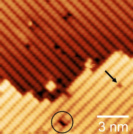
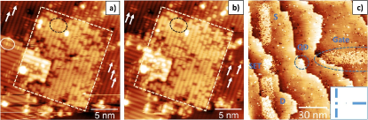
A fully terminated Cl-Si(100)-(21) surface can be seen in the representative filled-state STM image shown in Fig. 1. The image was acquired with the sample at 400 K after a Cl saturation exposure on a lower doped substrate. Cl2 dissociatively chemisorbs on Si(100) and each adsorbed Cl atom terminates the dangling bond of a single Si atom, maintaining the (21) reconstruction of the bare surfaceLyubinetsky et al. (1998). A single atomic-height step runs through the middle of the image and several common defects are identified including single Cl vacancies (arrow) and a single Si dimer vacancy (circle). With the exception of the Cl vacancies, each Si dimer is fully Cl-terminated.
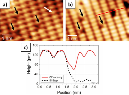
Cl was selectively desorbed from the surface using voltage pulses between the tip and sample. Figure 2 depicts successive filled-state STM images of the Cl-Si(100) surface of a lower doped substrate at room temperature (a) before and (b) after a 500 s voltage pulse of 4.25 V was applied to the sample. Prior to the pulse, the tunneling current setpoint, , was set to 0.5 nA with 1.6 V and the STM feedback was disabled. The black arrows identify three defects that remained stationary during successive imaging and serve as points of reference. The voltage pulse was executed at the Cl-terminated dimer marked with the white arrow in Fig. 2(a). Immediately following the pulse, two single atom-sized vacancies appeared on neighboring Si dimers along the same dimer row, as shown in Fig. 2(b). Imaging also improved in sharpness from the elimination of a slight double-tip imaging artifact that was potentially due to the transfer of Cl to the tip, similar to H transferLabidi et al. (2017); Huff et al. (2017). Figure 2(c) displays a line profile of the defect (solid line) taken along the solid line in Fig. 2(b), which is compared to the line profile of a nearby single atomic-height step (dashed line) within the same data set (not shown). We found the apparent step height to be approximately 1.3 Å, close to the expected value of 1.36 Å. After adjusting for this height calibration error, we found the apparent depth of the vacancy structure created by the voltage pulse to be approximately 0.83 Å, less than that of a Si step. Additionally, the configuration of the created vacancy structures correspond well with those reported for halogen vacancies located on neighboring Si dimersNakayama et al. (2002a); Trenhaile et al. (2006a). We conclude that the pulse generated multiple Cl-atom vacancies and that Si was not removed from the site.
The vacancy structure created in Fig. 2 is highly suggestive of a recombinative Cl2 desorption process stimulated by the electrons injected from the STM tip. The arrangement of the Cl vacancies on neighboring Si dimers along the same dimer row is similar to that observed for the recombinative desorption of H2 from H-Si(100)Dürr et al. (2002). Cl2 does not typically desorb from the surface by thermal, photon, or electron stimulation, and, as such, the desorption of Cl2 from Cl-Si(100) has not been fully studiedKota et al. (1998). Instead, Cl is removed from the surface as SiCl2 and SiCl4 via etching processesGao et al. (1993); Aldao and Weaver (2001); Jackman et al. (1989) and, to a lesser extent, as atomic Cl through a phonon-activated, electron-stimulated desorption process that is active near one monolayer halogen coveragesTrenhaile et al. (2005, 2006a). While we can conclude that Cl vacancies were created by the pulse, further investigation is required to determine the specific reaction mechanisms.
In addition to positive pulses, in which desorption is facilitated via electron injection, we found that negative pulses, which correspond to hole injection, also induced desorption. Figure 3 shows successive filled-state STM images (a) before and (b) after a 500 s voltage pulse of 5.5 V was applied to the Cl-Si(100) surface of a lower doped substrate at 600 K. was set to 0.1 nA with 1.0 V prior to the pulse. Black arrows identify three defects initially present on the surface, which serve as reference points. In contrast to the reference features identified in Fig. 2 (black arrows), we observed these features undergoing intradimer hopping from one side of the Si dimer to the other in subsequent images at 600 K. This hopping is apparent when comparing defect positions in Fig. 3(a) and (b). The white arrows identify similar features that appear in the same position in both images, although they may still be hopping in between images. While thermal drift at 600 K prevents us from knowing the exact pulse location, we observed a cluster of vacancies extending out roughly 3 nm from the presumed pulse site located at the highest concentration of vacancies in Fig. 3(b). This negative pulse created a total of 13 Cl vacancies consisting of a mixture of single, isolated Cl vacancies as well as Cl di-vacancies, i.e., bare Si dimers. We observed similar results from comparable pulses, with many vacancies being created over a span of several nanometers.
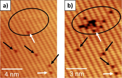
The spatial extent of the stimulated reactions observed in Fig. 3(b) is in qualitative agreement with similar results of non-local atomic manipulation of adsorbates on Si(111) via hole injectionRusimova et al. (2016); Lock et al. (2015); Sloan et al. (2010). While the reactions reported in Ref. 33 extend out tens of nanometers, we find hole injection induces reactions over a shorter length scale, presumably due to the much shorter pulse times reported here. We do not believe that the spatial extent of the vacancy complexes are due to outward vacancy diffusion since the neighboring single-atom vacancies remain stationary. If there was sufficient energy to drive outward diffusion, there would be sufficient energy to enable neighboring vacancies to pair in a more stable configuration on a single dimer, effectively gaining 0.4 eV in energy due to the formation of a Si-Si bondBoland (1991). Again, we are unable to definitively conclude from our results whether or not the negative voltage pulse induced the desorption of single Cl atoms, Cl2 molecules, or a mixture of both, but the creation of an odd number of vacancies is suggestive of an active single-atom desorption mechanism.
Although STM-induced desorption of single H atoms has been demonstratedMøller et al. (2017); Hersam et al. (2000), it was presumed to be too energetically costly to desorb Cl atoms from the surface due to the larger bonding energy of Si-Cl (4.7 eV) compared to Si-H (3.1 eV)Dean and Lange (1999). Single Cl atoms can also excite into one of several metastable adsorption sites, such as the dimer bridge bond or a Si-Si back-bond, to produce inserted Cl atoms, Cl(i), and a dangling bond on the surfacede Wijs and Selloni (1996); de Wijs et al. (1998); Boland (1993). Pairs of Cl(i) have a clearly defined STM signature, appearing as “bright” features extending across multiple dimer rowsAgrawal et al. (2007); Aldao et al. (2009). The absence of these bright features in our data suggests that the creation of dangling bonds is due to Cl desorption and not conversion to Cl(i). However, we cannot completely rule out the latter since the low diffusion barrier (0.3 eV to 0.4 eV) from one inserted site to anotherde Wijs et al. (1998) is more easily overcome at these elevated temperatures, enabling Cl(i) to reach a more stable adsorption site at a stepButera et al. (2009).
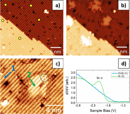
Further evidence of the absence of Cl(i) on the surface was obtained at 4 K where we expect Cl(i) diffusion to be frozen out. Additionally, Cl desorption was speculated to be more efficient at low temperature, as is the case for H-Si(100)Foley et al. (1998). Figure 4 shows several filled-state images of Cl-Si(100) surfaces at a sample temperature of 4 K. These were obtained on high-purity Si epilayer substrates using the cryogenic STM systemDreyer et al. (2010). Figure 4(a) and (b) are successive images taken before and after was ramped from 3.5 V to 10.0 V and back with 0.03 nA at the five locations marked by dots in (a). The ramp time was roughly 1 s and the max current read several nanoamperes. These ramps resulted in five bright areas on the surface corresponding to Cl-free, bare Si dimers. The voltage threshold for desorption was found to be higher at low temperature since no desorption was observed for ramps less than 10.0 V. STM spectroscopy was used to verify the surface termination of a bright area shown in Fig. 4(c), which was created using a ramp similar to the one used in Fig. 4(b). Figure 4(d) shows averaged dd measurements taken from a presumed Cl-terminated area (arrow 1 in (c)) as well as the bright area (arrow 2 in (c)). As seen in Fig. 4(d), a peak at approximately 2 V is present in the dd spectrum from the bright area (dotted line), indicative of the Si bond formed on the bare Si dimerNakayama et al. (2006). The position of this peak at 2 V is due to the low doping of the substrate. The spectrum from the Cl-terminated area (solid line) is linear and shows no -bond peak, verifying that the bright area was bare Si while the surrounding darker areas remained Cl terminated. Further, buckled dimers visible within the dashed circle in the bright area are also indicative of bare Si. At 4 K, we did not observe any evidence of nearby Cl(i), and thus we conclude that Cl was completely removed from the surface and not converted to Cl(i).
The bright appearance of the bare Si dimers seen in Fig. 4(b) and (c) is in contrast to the dark appearance of the Cl vacancy features in Fig. 2 and Fig. 3. Unlike the H-Si(100) surface, where H vacancies (bare Si) appear bright compared to surrounding H-terminated areas, Cl vacancies can appear either dark or bright depending on scanning conditions and whether the defects are single vacancies (typically dark in filled-state imaging) or di-vacancies, i.e., bare dimers (typically bright in filled-state imaging)(Lee and Kang, 2004). Sample temperature may also play a role in imaging these defects. In Fig. 4(b) and (c), multiple bare dimers are aligned together on several dimer rows resulting in the bright appearance of the desorbed patches, while the Cl vacancy cluster in Fig. 3(b) consists mostly of single vacancies.
In order for Cl to be a viable resist for device fabrication via STM lithography, it is necessary to pattern relatively large areas and remove a sufficient amount of Cl to enable adsorption of the precursor molecule. Lithographic patterning of H-Si(100) is routinely done at room temperature; however, we found patterning Cl-Si(100) to be more facile at elevated temperatures. This is likely due to the larger bonding energy of Si-Cl compared to Si-H. Figure 5 shows filled-state images demonstrating STM lithography on Cl-Si(100) in a field emission patterning mode utilizing a positive . This lithography was done while the sample was at a temperature of 400 K on a higher doped substrate. Figure 5(a) and (b) are successive filled-state STM images after lithographically patterning a 10 nm by 10 nm square area. The square was produced with 9.0 V, 1 nA, and 10 mC/cm (write speed of 1 nm/s) while the STM tip moved along every other dimer row of the patterned area in a serpentine mannerBallard et al. (2014a). The electron dose, , used here represents the total number of electrons delivered per unit length along the line (units of mC/cm) and sets the write speed for a given setpoint value.
Here, as in Fig. 4, Cl-free dimers appear bright. Remnant Cl atoms found within the patterned area from incomplete depassivation tend to pair, forming fully Cl-terminated dimers with a darkened appearance. The pattern is continuous across the single atomic-height step located on the left-hand side of the image. The dashed box roughly outlines the patterned area serving as a marker for pattern fidelity. Figure 5(b) shows that over several successive scans, the general dimensions of the pattern did not change. Diffusion of adsorbed Cl atoms into the patterned area from the surrounding edges is not significant at these slightly elevated temperatures. Numerous spurious bare Si dimers are visible outside the patterned area extending several nanometers away from the pattern edges. While positive field emission patterning is relatively quick and can cover a large area, it suffers from stochastic desorption events relatively far from the tip location. The desorption of Cl outside of the intended area is akin to spurious H desorption observed during STM patterning of H-Si(100)Ballard et al. (2014b). Isolated Cl di-vacancies, such as the one highlighted by the solid oval in Fig. 5(a), appear as a bright triplet feature at modest scan biasesNakayama et al. (2002a); Lee and Kang (2004). While the main pattern remained intact at elevated temperatures, individual Cl di-vacancies were observed diffusing along the dimer rows outside of the pattern, as indicated by the white arrows in Fig. 5(a) and (b).
At 400 K, we also observed intradimer hopping of Cl atoms within patterned areas. Intradimer hopping is imaged by the STM as a blurred feature with lobes at both ends of the Si dimer. It is the result of a single Cl atom hopping from one side of a Si dimer to the other at a rate much faster than the image acquisition time. The barrier for intradimer hopping was previously found to be approximately 0.6 eVde Wijs and Selloni (1996) and this process was shown to be facilitated by an STM tip under normal imaging conditionsNakamura et al. (2003). In contrast, the activation barrier for interdimer diffusion is 1.1 eVde Wijs and Selloni (1996). We did observe the pairing of several neighboring Cl atoms, visible as the blurred dimers in the dashed oval in Fig. 5(a), to create fully Cl-terminated dimers, appearing dark within the dashed oval in Fig. 5(b). The decay of a Cl-terminated dimer into two neighboring Cl atoms undergoing intradimer hopping was also observed.
Figure 5(c) shows field emission patterning in a larger area. A mock-up of a quantum device including a quantum dot island (QD), an electrostatic gate, and a single electron transistor (SET) charge sensor was patterned. The inset shows the intended pattern. This pattern was created using similar parameters as those used in Fig. 5(a).
In an effort to better understand and optimize field emission lithography of Cl, we patterned sets of lines while independently varying , , and and compared the resulting pattern line widths. Figure 6 is a filled-state image depicting a set of six lines lithographically patterned with varying values at 400 K on a higher doped substrate. Several of the lines can be seen going over the single atomic steps in the surface. Each line was written with 5 nA and 15 mC/cm while varying from 7.5 V to 10.0 V in steps of 0.5 V. Qualitatively, the widths of the lines in Fig. 6 appear larger at higher values. Quantitatively, the line widths were measured by averaging the profiles across a given line over the length of the line and then extracting the full width at half max of that averaged height profile. The measured width of the line patterned with bias in Fig. 6 is represented by the dashed box around the pattern. The line widths increase from 4.6(5) nm for 7.5 V to 7.9(5) nm for 10.0 V.
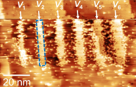
Figure 7 displays the measured widths of several sets of lithographic lines patterned at 400 K as a function of (a) positive , (b) sample temperature, (c) , and (d) . Linear fits to each data set (lines) are also shown. The measured line widths in Fig. 7(a) are shown to increase linearly with across multiple lithographic parameters. ranged from 1 nA to 20 nA and ranged from 10 mC/cm to 100 mC/cm. The slopes of each linear fit are consistent across the data, although there are clear offsets between the data sets. Table 1 displays the slopes and lithographic parameters for each data set in Fig. 7(a). The average slope of all the data sets in (a) is 1.7(2) nm/V. In comparison, a value of 2.2 nm/V was previously reported for H-terminated Si(100) depassivationLyding et al. (1996).
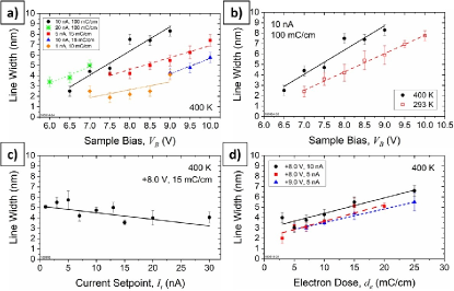
The positive correlation observed between line width and is consistent with the expectation that higher bias voltages cause the tip to retract slightly. Thus, electrons are field emitted from the tip in a wider angular distribution and with higher energies, leading to more desorption over a larger area. The offset of the different data sets appears to be partially correlated to the other parameters, with lower values resulting in smaller line widths (e.g., diamonds) for a given and vice versa. We also observed line width offsets between distinct data sets patterned using the same values of and , however the slopes remained consistent. These offsets are likely due to the sharpness and condition of the tip as well as the patterning alignment with the dimer rows. Extrapolating the fit slopes back to zero line width gives an approximate measure of the threshold bias value where Cl atoms receive enough energy to desorb from the surface. This fit-derived threshold bias ranges from 4.0 V to 7.5 V with an average of 5.4(4) V. These values are consistent with the typical positive values of 6.0 V to 6.5 V we observed for the onset of depassivation on Cl-Si(100) at elevated temperatures.
Figure 7(b) compares the widths of 400 K lines (circles) to those of lines patterned at room temperature (open squares). Both sets of lines were patterned with 10 nA and 100 mC/cm. The 400 K line widths are shifted to lower values relative to the room temperature line widths. While a shift may be the result of factors unrelated to temperature, such as changes in the tip, we saw a consistent shift to lower values at 400 K compared to room temperature. Moreover, at 4 K, a minimum of 10.0 V was needed to initiate desorption, indicating that the thermal energy of Cl on the surface plays a roll in desorption.
Figure 7(c) shows that line width weakly decreases with increasing . These data are the average of several sets of lines patterned at 400 K with 8.0 V and 15 mC/cm. The constant or weakly inverse correlation between line width and can be partly attributed to the tip moving closer to the surface as increases. This results in a narrower spread of emitted electrons. Additionally, while a higher current would presumably lead to more desorption events, a constant results in the write speed increasing at larger values, causing the tip to spend less time at each surface site.
Finally, Fig. 7(d) shows the line width dependence on for lines patterned at 400 K using values of 8.0 V and 9.0 V with values of either 5 nA or 10 nA. Two of the data sets (squares and triangles) are averages of several sets of measured lines. The measured line widths increase linearly with increasing . Both the line widths and the slopes of the fits are consistent across the data sets. Table 2 displays the slopes and lithographic parameters for each data set in Fig. 7(d). The average slope of the data in (d) is 0.15(2) nm/(mC/cm). Extrapolating previously reported electron dose data for depassivation of H-terminated Si(100) to our measurement range gives a similar line width dependence of approximately 0.22 nm/(mC/nm)Lyding et al. (1996). The positive correlation between line width and is consistent with the fact that at larger values, more electrons are injected over the same area leading to more chances for desorption events. Additionally, we observed that higher values resulted in more complete depassivation along the lithographic line, i.e., fewer Cl-terminated dimers remaining. The average depassivation fraction (bare Si dimer area over the total area) along lines presented in Fig. 7(d) increases from 0.72(3) for values of 3 mC/cm and 5 mC/cm up to 0.84(1) for values of 20 mC/cm and 25 mC/cm. For 3 mC/cm, we often observed little to no depassivation. For all the lines in Fig. 7 patterned using positive , the average depassivation fraction is 0.83(1), although depassivation increases away from the edges of lines and can be near unity around the center. While more complete depassivation may seem desirable, it is not necessary for lithographic features to be perfectly continuous to fabricate metallic regions via dopant incorporation. This is due to the large spatial extent of the dopant electronic states (2.5 nm Bohr radius for P), which can bridge the gap between narrow undoped regionsWeber et al. (2012).
At the lowest positive values used for desorption, no atomically precise patterning was observed. In contrast, an atomic precision patterning mode on H-Si(100) is active at values below the Cl desorption threshold bias we observed (e.g., 4.0 V). Interest in more precise patterning suitable for atomic-scale device fabrication led us to explore lithography with negative values. Negative biases have been used to induce the desorption of H via hole resonancesStokbro et al. (1998), and we found that hole injection induced desorption of Cl in a more confined, precise, and controllable manner than electron injection.
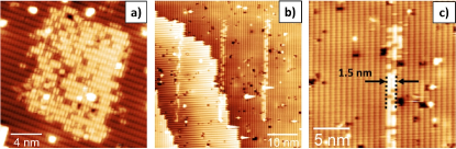
Figure 8 shows filled-state images demonstrating lithography on Cl-Si(100) using negative values in an atomic precision patterning mode. Lithography was done at 400 K on a higher doped substrate. A 15 nm by 15 nm square is shown in Fig. 8(a). It was patterned with 6.5 V, 10 nA, and 10 mC/cm while the tip traveled across dimer rows in a serpentine manner instead of along them as before. Due to incomplete depassivation, a few dark, Cl-terminated dimers within the patterned area can be seen forming some extended structures. The reduced desorption yield is due to the tip having moved across dimer rows during the specific patterning procedure used here, which we found to be less effective than moving along dimer rows. Interestingly, there are significantly fewer spurious bare dimers in the surrounding areas and the edges of the pattern are more abrupt and well defined than with positive values.
As a demonstration of atomic precision patterning, Fig. 8(b) shows three lines that vary in width from one to two dimer rows over most of the length of the lines, i.e, roughly 1.5 nm or less. Each is 25 nm in length and was patterned with 6.5 V and 10 mC/cm. The line on the left was patterned with 10 nA while the center and right lines were patterned with 100 nA. The center line was easily patterned across the atomic step running vertically through the middle of the image. The rightmost line and most of the center line were patterned with the write direction roughly aligned parallel with the dimer rows. A slight angular misalignment caused the pattern to drift one dimer row over in a couple spots causing the lines to be three dimer rows wide in these areas. In comparison, we found that the thinnest lines written with positive values had widths spanning three or four dimer rows with more inconsistent depassivation.
We found little to no spurious bare dimers appearing away from the lines patterned along the dimer rows. In contrast, the leftmost line was patterned with the write direction perpendicular to the dimer rows due to the presence of the step. In this case, spurious bare dimers appeared several nanometers on either side of the lines, as can be seen upon close examination of the leftmost line in Fig. 8(b). The narrowness of these lines is also clearly displayed in Fig. 8(c), which depicts the rightmost line from Fig. 8(b). The lines here are not fully continuous due to Cl remaining along the path of the lithography, which appear as several darker, Cl-terminated dimers. The average depassivation fraction of Si dimers along these three lines is 0.66(4).
Lithographic parameters for this atomic precision, negative mode were varied in a manner similar to the studies represented in Fig. 7, however, we found inconsistent or no dependence of the line widths on , , or . Additionally, no dependence on those lithographic parameters was found for the depassivation fraction along the lines. The average line width across all of the patterned lines studied here was measured to be 1.74(7) nm, which corresponds to 2.26(9) dimer row widths. The average depassivation fraction for all of the patterned lines produced using the range of lithographic parameters explored here was 0.68(2), lower than that of positive lines (0.83(1)). Ultimately, we found that the STM tip played a major role in the patterning precision when using negative values. Further studies are needed to better explore the lithography parameter phase space for atomic precision patterning, but it is clear that negative patterning is robust within a wide range of lithography conditions making it a highly valuable tool for fabrication of atomic scale devices on Cl-Si(100).
III Conclusion
We have demonstrated STM-induced desorption and lithographic patterning of Cl-terminated Si(100)-(21) from 4 K to 600 K. Elevated temperatures were found to aid in the Cl desorption process. Lithographically defined patterns were relatively stable up to 600 K, potentially enabling selective area deposition at elevated temperatures. We utilized positive values for field emission patterning useful for patterning large areas and demonstrated atomic precision patterning with negative values where Cl is desorbed from one to two dimer rows. Varying positive lithographic patterning parameters revealed that line widths are positively correlated with and , while the feature sizes of negative patterning were largely independent of these parameters. The results presented here clearly demonstrate the viability of Cl as a patternable resist on Si(100), furthering the development of halogen-based chemistries for atomic-precision, advanced-manufacturing applications.
We expect similar STM patterning behavior on bromine- and iodine-terminated Si(100)-(21), and investigations are underway to explore these heavier halogens as patternable resists. Both Br and I are less tightly bound to Si than Cl and, as such, have the potential to result in a more efficient patterning processXu et al. (2005a). I is mobile at room temperature on Si(100)Xu et al. (2005a), but at half-monolayer coverage, it is locked into a self-assembled c(42) patternXu et al. (2005b) with every other Si dimer I-terminated. These self-assembled patterns have the potential to serve as templates for targeted adsorption into a periodic array on H-Si(100)Ferng et al. (2009) or Cl-Si(100). We continue to explore the phase space of lithographic parameters to enable patterning of complex designs such as atomic-scale devices utilizing halogen-based acceptor chemistries such as BCl3 or AlCl3.
IV Experimental Methods
The experiments were performed in two separate UHV STM systems. Room temperature (approximately 293 K) and elevated temperature experiments up to 600 K were performed in a UHV chamber with a base pressure of Pa ( Torr) using a ScientaOmicron VT-STM with a ZyVector STM Lithography control system. This STM allows for a maximum bias voltage, , of 10.0 V to be applied to the sample stage. The Si(100) wafers used were p-type, B-doped with either 0.001 cm to 0.002 cm or 1 cm to 10 cm and were oriented within 0.5∘ of (100). Si samples were cut to 4 mm by 12 mm in size, mounted on a ScientaOmicron XA sample plate, and loaded into the UHV chamber. Clean Si(100)-(21) surfaces were prepared by flash annealing them in UHV to 1200 ∘C, following the procedure found in Ref. 58. Shortly after clean surface preparation, the samples were exposed to a flux of Cl2 to achieve a Cl-terminated surface. Cl2 was generated from a solid-state, electrochemical cell consisting of AgCl doped with 5 wt % CdCl2Spencer et al. (1983).
| data set | (nA) | (mC/cm) | (nm/V) |
| circles | 10 | 100 | 2.3(3) |
| stars | 20 | 100 | 1.6(5) |
| squares | 5 | 15 | 1.2(2) |
| triangles | 10 | 15 | 1.5(3) |
| diamonds | 1 | 10 | 0.8(4) |
| H-Si(100) (Ref. 52) | 0.1 | 0.54 | 2.2 |
Cl exposures were done with the sample at roughly 600 K to minimize water contamination and limit Cl atom insertion into the surfaceYu et al. (2008); Trenhaile et al. (2006b); Butera et al. (2009); Aldao et al. (2009). This temperature was sufficient to ensure that any Cl(i) generated as a result of the chemisorption process can diffuse and attach at a dangling bondAgrawal et al. (2007); Aldao et al. (2009); Butera et al. (2009), but low enough to prevent activation of etching and roughening processesNakayama et al. (2002b); Aldao and Weaver (2001). During Cl2 exposure, the pressure in the chamber remained below Pa ( Torr).
The elevated sample temperatures on the STM stage were controlled by a LakeShore 335 temperature controller and monitored by means of a Pt-100 resistor mounted on the stage. Samples were left to equilibrate for at least one hour after each temperature change prior to imaging and lithography to minimize thermally induced drift. Lithographic patterning of the Cl-Si(100) surfaces was done by defining , , and within ZyVector scrips that generate and execute box and line patterns aligned to the Si(100) dimer rows. Voltage pulsing was executed with STM feedback turned off after pulse parameters were set. For box and line patterns, feedback remained on during lithography. Boxes were patterned in a serpentine manner with the tip moving in the long axis either along (parallel) or across (perpendicular) dimer rowsBallard et al. (2014a). Lithographic parameters and fit slopes, , for sets of lines used to measure line width dependence on and are given in Table 1 and Table 2, respectively. Line widths were determined by taking the full width at half max of the average line profiles across each patterned line.
Low-temperature experiments were performed using a separate cryogenic STM system. This system is home built and consists of a UHV sample preparation chamber with a base pressure Pa ( Torr) and a cryogenic STM stage with a base temperature of 4.2 KDreyer et al. (2010). The sample used for these experiments consisted of a 1.5 m thick, high-purity intrinsic Si epilayer grown using molecular beam epitaxy on a highly P-doped Si(100) substrate with 0.0015 cm. The substrate was annealed to promote diffusion of dopants into the intrinsic Si layer. The sample surface and Cl-termination were prepared in the UHV chamber in a similar manner as in the other system mentioned earlier before transferring the sample to the cryogenic STM stage for low-temperature measurements including lithography and STM spectroscopy.
| data set | (V) | (nA) | (nm/(mC/cm)) |
| circles | 8.0 | 10 | 0.15(3) |
| squares | 8.0 | 5 | 0.16(2) |
| triangles | 9.0 | 5 | 0.13(2) |
| H-Si(100) (Ref. 52) | 6.0 | 0.1 | 0.22 |
V acknowledgement
The authors thank C. J. K. Richardson (Laboratory for Physical Sciences) for providing the Si epilayer substrate used for low-temperature measurements.
References
- Walsh and Hersam (2009) M. A. Walsh and M. C. Hersam, Annu Rev. of Phys. Chem. 60, 193 (2009).
- Ballard et al. (2014a) J. B. Ballard, J. H. G. Owen, W. Owen, J. R. Alexander, E. Fuchs, J. N. Randall, J. R. Von Ehr, S. McDonnell, D. D. Dick, R. M. Wallace, Y. J. Chabal, M. R. Bischof, D. L. Jaeger, R. F. Reidy, J. Fu, P. Namboodiri, K. Li, and R. M. Silver, J. of Vac. Sci. & Tech. B 32, 041804 (2014a).
- Shen et al. (1995) T. C. Shen, C. Wang, G. C. Abeln, J. R. Tucker, J. W. Lyding, P. Avouris, and R. E. Walkup, Science 268, 1590 (1995).
- Abeln et al. (1998) G. C. Abeln, M. C. Hersam, D. S. Thompson, S.-T. Hwang, H. Choi, J. S. Moore, and J. W. Lyding, J. of Vac. Sci. & Tech. B 16, 3874 (1998).
- Owen et al. (2011) J. H. G. Owen, J. Ballard, J. N. Randall, J. Alexander, and J. R. Von Ehr, J. of Vac. Sci. & Tech. B 29, 06F201 (2011).
- Warschkow et al. (2016) O. Warschkow, N. J. Curson, S. R. Schofield, N. A. Marks, H. F. Wilson, M. W. Radny, P. V. Smith, T. C. G. Reusch, D. R. McKenzie, and M. Y. Simmons, J. Chem. Phys. 144, 014705 (2016).
- Fuechsle et al. (2012) M. Fuechsle, J. A. Miwa, S. Mahapatra, H. Ryu, S. Lee, O. Warschkow, L. C. L. Hollenberg, G. Klimeck, and M. Y. Simmons, Nat. Nanotechnol. 7, 242 (2012).
- Broome et al. (2018) M. A. Broome, S. K. Gorman, M. G. House, S. J. Hile, J. G. Keizer, D. Keith, C. D. Hill, T. F. Watson, W. J. Baker, L. C. L. Hollenberg, and M. Y. Simmons, Nat. Commun. 9, 980 (2018).
- Salfi et al. (2014) J. Salfi, M. Tong, S. Rogge, and D. Culcer, Nanotechnology 27, 244001 (2014).
- Salfi et al. (2016) J. Salfi, J. A. Mol, D. Culcer, and S. Rogge, Phys. Rev. Lett. 116, 246801 (2016).
- Shim and Tahan (2014) Y.-P. Shim and C. Tahan, Nat. Commun. 5, 4225 (2014).
- Blase et al. (2009) X. Blase, E. Bustarret, C. Chapelier, T. Klein, and C. Marcenat, Nat. Mater. 8, 375 (2009).
- Cammilleri et al. (2008) D. Cammilleri, F. Fossard, D. Débarre, C. T. Manh, C. Dubois, E. Bustarret, C. Marcenat, P. Achatz, D. Bouchier, and J. Boulmer, Thin Solid Films 517, 75 (2008).
- Ferguson et al. (2009) G. A. Ferguson, U. Das, and K. Raghavachari, J. Phys. Chem. C 113, 10146 (2009).
- Jung et al. (2008) S. Jung, Y.-S. Youn, H. Lee, K.-J. Kim, B. S. Kim, and S. Kim, J. Am. Chem. Soc. 130, 3288 (2008).
- Koleske et al. (1992) D. D. Koleske, S. M. Gates, and D. B. Beach, J. Appl. Phys. 72, 4073 (1992).
- Gates (1992) S. M. Gates, J. of Phys. Chem. 96, 10439 (1992).
- Mendicino and Seebauer (1993) M. A. Mendicino and E. G. Seebauer, J. Electrochem. Soc. 140, 1786 (1993).
- Pilli et al. (2018) A. Pilli, J. Jones, V. Lee, N. Chugh, J. Kelber, F. Pasquale, and A. LaVoie, Journal of Vacuum Science & Technology A 36, 061503 (2018).
- Mitsui et al. (1999) T. Mitsui, R. Curtis, and E. Ganz, J. Appl. Phys. 86, 1676 (1999).
- Pavlova et al. (2018) T. V. Pavlova, G. M. Zhidomirov, and K. N. Eltsov, J. Phys. Chem. C 122, 1741 (2018).
- Lyubinetsky et al. (1998) I. Lyubinetsky, Z. Dohnálek, W. J. Choyke, and J. T. Yates, Phys. Rev. B 58, 7950 (1998).
- Labidi et al. (2017) H. Labidi, M. Koleini, T. Huff, M. Salomons, M. Cloutier, J. Pitters, and R. A. Wolkow, Nature Communications 8, 14222 (2017).
- Huff et al. (2017) T. R. Huff, H. Labidi, M. Rashidi, M. Koleini, R. Achal, M. H. Salomons, and R. A. Wolkow, ACS Nano 11, 8636 (2017).
- Nakayama et al. (2002a) K. S. Nakayama, E. Graugnard, and J. H. Weaver, Phys. Rev. Lett. 89, 266106 (2002a).
- Trenhaile et al. (2006a) B. R. Trenhaile, V. N. Antonov, G. J. Xu, A. Agrawal, A. W. Signor, R. E. Butera, K. S. Nakayama, and J. H. Weaver, Phys. Rev. B 73, 125318 (2006a).
- Dürr et al. (2002) M. Dürr, A. Biedermann, Z. Hu, U. Höfer, and T. F. Heinz, Science 296, 1838 (2002).
- Kota et al. (1998) G. P. Kota, J. W. Coburn, and D. B. Graves, J. Vac. Sci. & Tech. A 16, 270 (1998).
- Gao et al. (1993) Q. Gao, C. Cheng, P. Chen, W. Choyke, and J. Yates, Thin Solid Films 225, 140 (1993).
- Aldao and Weaver (2001) C. Aldao and J. Weaver, Prog. Surf. Sci. 68, 189 (2001).
- Jackman et al. (1989) R. Jackman, R. Price, and J. Foord, Appl. Surf. Sci. 36, 296 (1989).
- Trenhaile et al. (2005) B. Trenhaile, V. Antonov, G. Xu, K. S. Nakayama, and J. Weaver, Surf. Sci. 583, L135 (2005).
- Rusimova et al. (2016) K. R. Rusimova, N. Bannister, P. Harrison, D. Lock, S. Crampin, R. E. Palmer, and P. A. Sloan, Nat. Commun. 7, 12839 (2016).
- Lock et al. (2015) D. Lock, K. R. Rusimova, T. L. Pan, R. E. Palmer, and P. A. Sloan, Nat. Commun. 6, 8365 (2015).
- Sloan et al. (2010) P. A. Sloan, S. Sakulsermsuk, and R. E. Palmer, Phys. Rev. Lett. 105, 048301 (2010).
- Boland (1991) J. J. Boland, Phys. Rev. Lett. 67, 1539 (1991).
- Møller et al. (2017) M. Møller, S. P. Jarvis, L. Guérinet, P. Sharp, R. Woolley, P. Rahe, and P. Moriarty, Nanotechnology 28, 075302 (2017).
- Hersam et al. (2000) M. C. Hersam, N. P. Guisinger, and J. W. Lyding, J. of Vac. Sci. & Tech. A 18, 1349 (2000).
- Dean and Lange (1999) J. A. Dean and N. A. Lange, Lange’s handbook of chemistry (McGraw-Hill, 1999).
- de Wijs and Selloni (1996) G. A. de Wijs and A. Selloni, Phys. Rev. Lett. 77, 881 (1996).
- de Wijs et al. (1998) G. A. de Wijs, A. De Vita, and A. Selloni, Phys. Rev. B 57, 10021 (1998).
- Boland (1993) J. J. Boland, Science 262, 1703 (1993).
- Agrawal et al. (2007) A. Agrawal, R. E. Butera, and J. H. Weaver, Phys. Rev. Lett. 98, 136104 (2007).
- Aldao et al. (2009) C. M. Aldao, A. Agrawal, R. E. Butera, and J. H. Weaver, Phys. Rev. B 79, 125303 (2009).
- Butera et al. (2009) R. E. Butera, Y. Suwa, T. Hashizume, and J. H. Weaver, Phys. Rev. B 80, 193307 (2009).
- Foley et al. (1998) E. T. Foley, A. F. Kam, J. W. Lyding, and P. Avouris, Physical Review Letters 80, 1336 (1998).
- Dreyer et al. (2010) M. Dreyer, J. Lee, H. Wang, and B. Barker, Review of Scientific Instruments 81, 053703 (2010).
- Nakayama et al. (2006) K. S. Nakayama, M. M. G. Alemany, T. Sugano, K. Ohmori, H. Kwak, J. R. Chelikowsky, and J. H. Weaver, Phys. Rev. B 73, 035330 (2006).
- Lee and Kang (2004) J. Y. Lee and M.-H. Kang, Phys. Rev. B 69, 113307 (2004).
- Ballard et al. (2014b) J. B. Ballard, J. H. G. Owen, J. D. Alexander, W. R. Owen, E. Fuchs, J. N. Randall, R. C. Longo, and K. Cho, J. of Vac. Sci. & Tech. B 32, 021805 (2014b).
- Nakamura et al. (2003) Y. Nakamura, Y. Mera, and K. Maeda, Surf. Sci. 531, 68 (2003).
- Lyding et al. (1996) J. W. Lyding, T.-C. Shen, G. C. Abeln, C. Wang, and J. R. Tucker, Nanotechnology 7, 128 (1996).
- Weber et al. (2012) B. Weber, S. Mahapatra, H. Ryu, S. Lee, A. Fuhrer, T. C. G. Reusch, D. L. Thompson, W. C. T. Lee, G. Klimeck, L. C. L. Hollenberg, and M. Y. Simmons, Science 335, 64 (2012).
- Stokbro et al. (1998) K. Stokbro, C. Thirstrup, M. Sakurai, U. Quaade, B. Y.-K. Hu, F. Perez-Murano, and F. Grey, Phys. Rev. Lett. 80, 2618 (1998).
- Xu et al. (2005a) G. Xu, A. Signor, A. Agrawal, K. S. Nakayama, B. Trenhaile, and J. Weaver, Surf. Sci. 577, 77 (2005a).
- Xu et al. (2005b) G. J. Xu, N. A. Zarkevich, A. Agrawal, A. W. Signor, B. R. Trenhaile, D. D. Johnson, and J. H. Weaver, Phys. Rev. B 71, 115332 (2005b).
- Ferng et al. (2009) S.-S. Ferng, S.-T. Wu, D.-S. Lin, and T. C. Chiang, J. Chem. Phys. 130, 164706 (2009).
- Trenhaile et al. (2006b) B. R. Trenhaile, A. Agrawal, and J. H. Weaver, Appl. Phys. Lett. 89, 151917 (2006b).
- Spencer et al. (1983) N. D. Spencer, P. J. Goddard, P. W. Davies, M. Kitson, and R. M. Lambert, J. Vac. Sci. & Tech. A 1, 1554 (1983).
- Yu et al. (2008) S.-Y. Yu, H. Kim, and J.-Y. Koo, Phys. Rev. Lett. 100, 036107 (2008).
- Nakayama et al. (2002b) K. S. Nakayama, E. Graugnard, and J. H. Weaver, Phys. Rev. Lett. 88, 125508 (2002b).