Large magneto-optical effects and magnetic anisotropy energy in two-dimensional Cr2Ge2Te6
Abstract
Atomically thin ferromagnetic (FM) films were recently prepared by mechanical exfoliation of bulk FM semiconductor Cr2Ge2Te6. They provide a platform to explore novel two-dimensional (2D) magnetic phenomena, and offer exciting prospects for new technologies. By performing systematic ab initio density functional calculations, here we study two relativity-induced properties of these 2D materials [monolayer (ML), bilayer (BL) and trilayer (TL) as well as bulk], namely, magnetic anisotropy energy (MAE) and magneto-optical (MO) effects. Competing contributions of both magneto-crystalline anisotropy energy (C-MAE) and magnetic dipolar anisotropy energy (D-MAE) to the MAE, are computed. Calculated MAEs of these materials are large, being in the order of 0.1 meV/Cr. Interestingly, we find that the out-of-plane magnetic anisotropy is preferred in all the systems except the ML where an in-plane magnetization is favored because here the D-MAE is larger than the C-MAE. Crucially, this explains why long-range FM order was observed in all the few-layer Cr2Ge2Te6 except the ML because the out-of-plane magnetic anisotropy would open a spin-wave gap and thus suppress magnetic fluctuations so that long-range FM order could be stabilized at finite temperature. In the visible frequency range, large Kerr rotations up to 1.0∘ in these materials are predicted and they are comparable to that observed in famous MO materials such as PtMnSb and Y3Fe5O12. Moreover, they are 100 times larger than that of 3 transition metal MLs deposited on Au surfaces. Faraday rotation angles in these 2D materials are also large, being up to 120 deg/m, and are thus comparable to the best-known MO semiconductor Bi3Fe5O12. These findings thus suggest that with large MAE and MO effects, atomically thin Cr2Ge2Te6 films would have potential applications in novel magnetic, MO and spintronic nanodevices.
I Introduction
Two-dimensional (2D) materials are layer substances with a thickness of one or few atomic or molecular monolayers (MLs). The vibrant field of 2D materials was triggered by the first isolation of graphene, a single atomic layer of graphite with carbon atoms arranged in a 2D honeycomb lattice, through mechanical exfoliation of graphite and also the discovery of its extraordinary transport properties in 2004. novoselov2004 The recent intensive interest in graphene has also stimulated research efforts to fabricate and investigate other 2D materials. miro2014 ; bhimanapati2015 Many of these 2D materials exhibit a variety of fascinating properties not seen in their bulk counterparts due to, e.g., symmetry breaking and quantum confinement. For example, a semiconductor MoS2 crystal was found to exhibit an indirect to direct bandgap transition when thinned down to a ML. mak2010 Importantly, the broken inversion symmetry makes MLs of MoS2 and other transition metal dichalcogenides exhibit novel properties of fundamental and technological interest such as spin-valley coupling xiao2012 , piezoelectricity duerloo2012 and second-harmonic generation wang2015 .
More recently, the family of 2D materials has also been extended to 2D magnets, crucial for the development of magnetic nanodevices and spintronic applications. For example, realization of 2D magnets by doping transition metals into nonmagnetic parent monolayers has been predicted by ab initio density functional calculations and also attempted experimentally by numerous research groups bhimanapati2015 . Hole-doping into a GaSe ML which possesses a unique van Hove singularity near the top of its valance band, was recently predicted to induce tunable ferromagnetism and magneto-optical effects gao2015 ; feng2016 . Experimental and theoretical evidence for the ferromagnetic (FM) MoS2 ML at the MoS2/CdS interface was also reported. tan2016 Several layered magnetic compounds have recently been investigated theoretically to determine whether their structure and magnetism can be retained down to ML thickness.li2014 ; zhang2015b ; sivadas2015 ; lin2016 These intensive research efforts finally led two groups to successfully thin bulk ferromagnets CrI3 and Cr2Ge2Te6 down to few-layer ultrathin films and to observe the intrinsic ferromagnetism retained in one and two monolayers, respectively.huang2017 ; gong2017 This successful fabrication of 2D magnets would allow us to study 2D magnetism and exotic magnetic phenomena, and also offers exciting prospects for advanced technological applications.
In this paper, we focus on two relativity-induced properties of atomically thin FM Cr2Ge2Te6 filmsgong2017 , namely, magnetic anisotropy energy (MAE) and magnet-optical (MO) effects. For comparison, we also consider bulk Cr2Ge2Te6, which is interesting on its own right. Bulk Cr2Ge2Te6 belongs to the rare class of intrinsic FM semiconductors carteaux1995 and has recently been attracting renewed interest because of its layered, quasi-2D FM structure with weak van der Waals bonds. For example, its magnetic anisotropy energy was recently measured. zhang2016 It was also used as a substrate for epitaxial growth of topological insulator Bi2Te3 to realize quantum anomalous Hall effect ji2013 .
Magnetic anisotropy energy refers to the total energy difference between the easy- and hard-axis magnetizations, i.e., the energy required to rotate the magnetization from the easy to the hard direction. Together with the magnetization and magnetic ordering temperature, MAE is one of the three important parameters that characterizes a FM material. Furthermore, MAE is especially important for 2D magnetic materials such as few-layer Cr2Ge2Te6 structures because it helps to lift the Mermin-Wangner restriction Mermin66 , thus allowing the long-range ferromagnetic order to survive at finite temperature even in the ML limit huang2017 . Moreover, 2D magnets with a significant MAE would find spintronic applications such as high density magnetic memory and data-storage devices. MAE consists of two contributions, namely, the magnetocrystalline anisotropy energy (C-MAE) due to the effect of relativistic spin-orbit coupling (SOC) on the electronic band structure, and also the magnetic dipolar (shape) anisotropy energy (D-MAE) due to the magnetostatic interaction among the magnetic moments Guo91b ; Tung07 . Note that the D-MAE always prefers an in-plane magnetization. Guo91b Although the D-MAE in isotropic bulk materials is generally negligibly small, the D-MAE could become significant in low-dimensional materials such as magnetic monolayers Guo91b and atomic chains Tung07 . Despite of the recent intensive interest in few-layer Cr2Ge2Te6, li2014 ; zhang2015b ; sivadas2015 ; lin2016 ; gong2017 ; tian2016 ; xing2017 no investigation into their MAE has been reported, although an experimental measurement on MAE zhang2016 and a theoretical calculation of C-MAE gong2017 of bulk Cr2Ge2Te6 were recently reported. Therefore, in this paper we carry out a systematic ab initio density functional investigation into the MAE as well as other magnetic properties of bulk and few-layer Cr2Ge2Te6. Furthermore, both C-MAE and D-MAE are calculated here. Importantly, as will be reported in Sec. III, taking the D-MAE into account results in an in-plane magnetization for the Cr2Ge2Te6 ML while all other considered Cr2Ge2Te6 materials have the out-of-plane magnetic anisotropy. Thus, this interesting finding could explain why the ferromagnetism was not observed in the Cr2Ge2Te6 ML. gong2017
Magneto-optical Kerr effect (MOKE) and Faraday effect (MOFE) are two well-known MO effects. Oppeneer2001 ; antonov2004 When a linearly polarized light beam hits a magnetic material, the polarization vector of the reflected and transmitted light beams rotates. The former and latter are known as Kerr and Faraday effects, respectively. Faraday effect has attracted much less attention than Kerr effect simply because light can only transmit through ultrathin films. In contrast, MOKE has been widely used to study magnetic and electronic properties of solids including surfaces and films. antonov2004 Furthermore, magnetic materials with large MOKE would find valuable MO storage and sensor applications mansuripur95 ; castera96 , and hence have been continuously searched for in recent decades. The recent development of 2D magnetic materials huang2017 ; gong2017 offers exciting possibilities of scaling the MO storage and sensing devices to the few-nanometer scale. However, detection and measurement of magnetism in these 2D materials will be difficult by using traditional methods such as superconducting quantum interference device (SQUID) magnetometer because ultrahigh sensitivity would be required for these ultrathin films. In this regard, MOKE and MOFE are a powerful, nonevasive probe of spontaneous magnetization in these 2D materials. Indeed, long-range ferromagnetic orders in both Cr2Ge2Te6 and CrI3 atomically thin films were detected by using the MOKE technique. gong2017 ; huang2017 ; xing2017 In this paper, therefore, we perform a systematic ab initio density functional study of the magneto-optical and optical properties of bulk and atomically thin films of Cr2Ge2Te6. Indeed, we find that both the bulk and the ultrathin films would exhibit large MOKE with Kerr rotation angles being as large as 1.0 ∘. Furthermore, the calculated Faraday rotation angles of the thin films are also large, being 120 deg/m. Therefore, bulk and ultrathin films Cr2Ge2Te6 are promising magneto-optical materials for high-density MO recordings and magnetic nanosensors.
II STRUCTURES AND METHODS
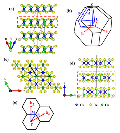
In this paper, we study the electronic, magnetic, and magneto-optical properties of few-layer and bulk Cr2Ge2Te6 structures. Bulk Cr2Ge2Te6 forms a layered structure with MLs separated by the so-called van der Waals (vdW) gap [Fig. 1(a)].carteaux1995 Each Cr2Ge2Te6 ML consists of two AB-stacked compact hexagonal Te planes with one Ge dimer lying vertically at one of every three hexagon centers [Fig. 1(c)] and two Cr atoms occupying two of every three Te octohedron centers [Figs 1(a), (c) and (d)]. These layers are ABC stacked [Fig. 1(a)], thus resulting in a rhombohedral symmetry with one chemical formula unit (f.u.) per unit cell. The experimental lattice constants are Å. carteaux1995 . This structure can also be regarded as an ABC-stacked hexagonal crystal cell with experimental lattice constants Å and Å. carteaux1995 As explained in the next paragraph, we adopt the experimental rhombohedral unit cell in the bulk calculations, and for the few-layer Cr2Ge2Te6 structures, the hexagonal unit cell with the experimental bulk lattice constants and atomic positions [Fig. 1(c)]. For bilayer (BL) and trilayer (TL) Cr2Ge2Te6 structures, we consider the AB and ABC stackings, respectively, as observed in bulk Cr2Ge2Te6 [Fig. 1(d)]. The few-layer structures are modelled by using the slab-superlattice approach with the separations between MLs being at least 15 Å.
Ab initio calculations are performed based on density functional theory. The exchange-correlation interaction is treated with the generalized gradient approximation (GGA) parameterized by Perdew-Burke-Ernzerhof formula perdew1996generalized . To improve the description of on-site Coulomb interaction between Cr 3d electrons, we adopt the GGA+U scheme.dudarev98 It was reported in Ref. gong2017, that a physically appropriate value of the effective onsite Coulomb energy should be within the range of eV. Therefore, here we use eV (see also the supplementary note in the supplementary material (SM)SM for explanations). The accurate projector-augmented wave kresse1999ultrasoft method, as implemented in the Vienna ab initio Simulation Package (VASP) kresse1996efficient ; kresse1996efficiency , is used. A large plane wave cutoff energy of 450 eV is used throughout. For the Brillouin zone integrations, -point meshes of 16 16 16 and 20 20 1 are used for bulk and few-layer Cr2Ge2Te6, respectively. The structural optimization within the GGA+U scheme for bulk Cr2Ge2Te6 results in lattice constants Å and Å. This theoretical is more than 10 % larger than the experimental , although the calculated is only 1.5 % too large. This is because the GGA+U tends to largely overestimate the vdW gaps in layered materials. To account for the vdW dispersion interactions, we further perform the structural optimization with the GGA+U plus vdW-density functional of Langreth and co-workers Lee10 as implemented in the VASP, and obtain Å and Å. The discrepancy in between the calculation and experiment carteaux1995 is much reduced to -2.3 % but the calculated is still more than 1.0 % too large. The GGA+U structural optimization for ML Cr2Ge2Te6 results in Å, which deviates only slightly from the theoretical bulk (by less than 0.1 %). This shows that structural relaxations in ML Cr2Ge2Te6 is much smaller than the errors in the GGA+U and GGA+U+vdW correction schemes. Therefore, we use the experimentally determined bulk atomic structure in all the subsequent calculations.
To understand the magnetism and also estimate the magnetic ordering temperature (Tc) for bulk and few-layer Cr2Ge2Te6, we determine the exchange coupling parameters by mapping the calculated total energies of different magnetic configurations onto the classical Heisenberg Hamiltonian, where donates the nonmagnetic ground state energy; the exchange coupling parameter between sites and ; , the unit vector representing the direction of the magnetic moment on site . Specifically, the total energies of the four intralayer magnetic configurations for one Cr2Ge2Te6 layer can be expressed as a set of 4 linear equations of , and : , , and . Given the calculated total energies, one can solve this set of linear equations to obtain the , and values. Similarly, given the calculated and , one can obtain the value.
As described in Sec. I, magnetic anisotropy energy (MAE) consists of two parts, namely, magnetocrystalline anisotropy energy (C-MAE) and magnetic dipolar anisotropy energy (D-MAE). To determine C-MAE, we first perform two self-consistent relativistic electronic structure calculations for the in-plane and out-of-plane magnetizations, and then obtain the C-MAE as the total energy difference between the two calculations. Highly dense -point meshes of 25 25 25 and 30 30 1 are used for bulk and few-layer Cr2Ge2Te6, respectively. Test calculations using different -point meshes show that thus-obtained C-MAE converges within 1 %. For a FM system, the magnetic dipolar energy in atomic Rydberg units is given by Guo91b ; Tung07
| (1) |
where the so-called magnetic dipolar Madelung constant
| (2) |
which is evaluated by Ewald’s lattice summation technique. Ewald21 R are the lattice vectors and q are the atomic position vectors in the unit cell. The speed of light and is the atomic magnetic moment (in units of ) on site . Thus, given the calculated magnetic moments, the D-MAE is obtained as the difference in between the in-plane and out-of-plane magnetizations. In a 2D material, all the R and q are in-plane. Thus, the second term in Eq. (2) would be zero for the out-of-plane magnetization, thereby resulting in the positive while for an in-plane magnetization the are negative. For example, in ML Cr2Ge2Te6, the calculated () is 11.0246 (23.0628) for the out-of-plane magnetization and is -5.5123 (-11.5314) for an in-plane magnetization. Therefore, the D-MAE always prefers an in-plane magnetization in a 2D material. This is purely a geometric effect and consequently the D-MAE is also known as the magnetic shape anisotropy energy.
For a FM solid possessing at least a trigonal symmetry with the magnetization along the rotational -axis, the optical conductivity tensor can be reduced in the form,
| (3) |
We calculate the three independent elements of the conductivity tensor using the Kubo formula within the linear response theory. wang1974band ; Oppeneer92 ; feng2015large Here the adsorptive parts of these elements, i.e., the real diagonal and imaginary off-diagonal elements, are given by,
| (4) |
| (5) |
where is the photon energy, and is the th band energy at point . Summations and are over the occupied and unoccupied bands, respectively. Dipole matrix elements where denotes Cartesian component of the dipole operator, are obtained from the band structures within the PAW formalismAdolph01 , as implemented in the VASP package. The integration over the Brillouin zone is carried out by using the linear tetrahedron method (see Temmerman89 and references therein). The dispersive parts of the optical conductivity elements can be obtained from the corresponding absorptive parts using the Kramers-Kroing relations
| (6) |
| (7) |
where donates the principle value. To take the finite quasiparticle lifetime effects into account, we convolute all the optical conductivity spectra with a Lorentzian of line width . For layered vdW materials such as graphite, is about 0.2 eV (see, e.g., Figs. 1(a) and 1(b) in Ref. [Guo04, ]), which is thus used in this paper.
We should note that the optical conductivity calculated using Eqs. (4) and (5) is based on the independent-particle approximation, i.e., the many-body effects, namely, the quasi-particle self-energy corrections and excitonic effects, are neglected. These many-body effects on the optical properties of 2D systems such as MoS2 and SiC monolayers Qiu13 ; Hsueh11 are especially pronounced due to the reduced dimensionality. Nevertheless, here the self-energy corrections are taken into account by the scissors correction using the bandgaps from the hybrid functional HSE06 heyd2003j ; heyd2006 calculations, as reported in the next section (Sec. III.B), and the quasi-particle lifetime effects are accounted for by convoluting all the optical conductivity spectra with a Lorentzian, as mentioned above. Weak or moderate electron-hole interaction would merely enhance the peaks near the absorption edge Benedict98 . However, strong electron-hole interaction in, e.g., MoS2 monolayer, could give rise to additional prominent excitonic peaks below the absorption edge Qiu13 . Nonetheless, in contrast to direct bandgap MoS2 monolayer, all the Cr2Ge2Te6 systems considered here have an indirect bandgap and hence one could expect no strong excitonic effect on their optical and MO properties. Indeed, no excitonic transition peak was observed in ultrathin indirect band gap GaSe films in a very recent experiment Budweg17 .
Here we consider the polar MOKE and MOFE. For a bulk magnetic material, the complex polar Kerr rotation angle is given by guo1994 ; guo1995 ,
| (8) |
For a magnetic thin film on a nonmagnetic substrate, however, the complex polar Kerr rotation angle is given by feng2016 ; suzuki1992
| (9) |
where stands for the speed of light in vacuum; the thickness of the magnetic layer; () the diagonal part of the dielectric constant (optical conductivity) of the substrate. Experimentally, atomically thin Cr2Ge2Te6 films were prepared on SiO2/Si. gong2017 Thus, the optical dielectric constant of bulk SiO2 (3.9) is used as . Similarly, the complex Faraday rotation angle for a thin film can be written as ravindran1999
| (10) |
where and represent the refractive indices for left- and right-handed polarized lights, respectively, and are related to the corresponding dielectric function (or optical conductivity via expressions . Here the real parts of the optical conductivity can be written as
| (11) |
where . Clearly, , and this shows that would be nonzero only if and are different. In other words, magnetic circular dichroism is the fundamental cause of the nonzero and hence the magneto-optical effects.
III RESULTS AND DISCUSSION
III.1 Magnetic moments and exchange coupling
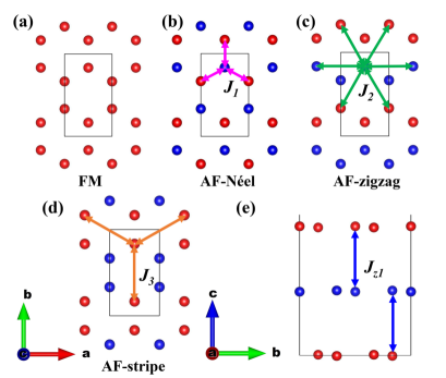
We consider four intralayer magnetic configurations for each Cr2Ge2Te6 ML comprising the FM as well as three antiferromagnetic (AF) structures, as labeled AF-Nel, AF-zigzag, and AF-stripe in Fig. 2. The FM state is found to be the ground state in all the considered materials. The lowest energy AF state is the AF-zigzag which is however more than 0.05 eV/f.u. higher in energy than the FM state in all the systems considered. For the bilayer, trilayer and bulk systems, we also consider the interlayer AF state [see Fig. 2(e)]. We find that the interlayer AF state is only slightly (i.e., a couple of meV/f.u.) above the interlayer FM state. Calculated spin and orbital magnetic moments of Cr2Ge2Te6 in the FM state are listed in Table I. The Cr spin magnetic moment in all the structures is 3.2 , being in good agreement with the experimental value of 3.0 ji2013 . This is consistent with three unpaired electrons in the Cr ionic configuration in these materials. The calculated Cr orbital magnetic moment is negligibly small (Table I), further suggesting that the Cr ions are in the configuration. Interestingly, the induced spin magnetic moment on the Te site is significant (0.15 ) and also antiparallel to that of the Cr atoms, although the spin moment on the Ge atom is five times smaller (Table I). This results in exactly 6.0 /f.u., and is in good agreement with the measured bulk magnetizationji2013 . The mechanism of ferromagnetism in all the Cr2Ge2Te6 structures could be attributed to the dominant FM superexchange coupling between half-filled Cr and empty states via Te orbitals, against the AF direct exchange interactions of Cr states.li2014 This is further supported by our finding of significant spin moments of Te atoms which are antiparallel to the Cr spin moments (Table I).
| structure | () | () | () | () | () | |||
|---|---|---|---|---|---|---|---|---|
| (/f.u.) | (/atom) | (/atom) | (/atom) | (meV/f.u.) | (meV/f.u.) | (eV) | (eV) | |
| monolayer | 6.00 | 3.23 (0.003) | 0.024 (0.001) | -0.144 (-0.003) | 0.107 (-0.153) | -0.05 | 0.23 | 0.56 |
| bilayer | 6.00 | 3.23 (0.003) | 0.024 (0.001) | -0.145 (-0.003) | 0.274 (-0.153) | 0.12 | 0.13 | 0.44 |
| trilayer | 6.00 | 3.23 (0.003) | 0.025 (0.001) | -0.145 (-0.001) | 0.297 (-0.153) | 0.14 | 0.09 | 0.41 |
| bulk | 6.00 | 3.23 (0.003) | 0.025 (0.001) | -0.146 (-0.003) | 0.471 (-0.067) | 0.40 (0.0511footnotemark: 1) | 0.04 (0.7422footnotemark: 2) | 0.33 |
Ref. zhang2016, . 22footnotemark: 2Ref. ji2013, .
Using the calculated total energies of the magnetic configurations considered here, we estimate the intralayer first-, second- and third-neighbor exchange coupling parameters (, , ) as well as the first-neighbor interlayer coupling constant () by mapping the total energies to the effective Heisenberg Hamiltonian model as described above in Section II. The estimated exchange coupling parameters are listed in Table II. The large, positive values in all the structures show that the nearest-neighbor Cr-Cr coupling is strongly ferromagnetic. In contrast, the second nearest neighbor coupling () is about 20 times weaker and antiferromagnetic. Interestingly, calculated values are three times larger than although they are about ten times smaller than . The calculated interlayer exchange coupling parameter () is about as large as but ferromagnetic. Table I shows that all the exchange interaction parameters increase monotonically with the increasing number of layers. This suggests that the magnetism is strengthened as one moves from the ML to the BL and eventually to the bulk. Our value agree quite well with that of the previous ab initio calculation ( meV) reported in Ref. li2014 . Nonetheless, all the present values appear to be about twice as large as that of the ab initio calculation of Ref. gong2017 , although the trends are very similar. This discrepancy in the calculated J values between Ref. [gong2017, ] and the present calculation could be attributed to the fact that the LSDA+U is used in Ref. [gong2017, ] while the GGA+U is exploited in this paper. This is because the LSDA tends to underestimate the tendency of magnetism. Note that for comparison of the previous ab initio calculationsli2014 ; gong2017 with the present results, the values reported in Refs. li2014 and gong2017 should be multiplied by a factor of .
III.2 Magnetic anisotropy energy and ferromagnetic transition temperature
| system | () | |||||
|---|---|---|---|---|---|---|
| (meV) | (meV) | (meV) | (meV) | (K) | (K) | |
| ML | 12.74 | -0.09 | 0.29 | - | 149 | 0 |
| BL | 14.26 | -0.47 | 1.07 | 0.40 | 169 | 71 (2811footnotemark: 1) |
| TL | 14.75 | -0.57 | 1.29 | 0.74 | 176 | 76 (3511footnotemark: 1) |
| bulk | 15.74 | -0.78 | 1.74 | 1.08 | 189 | 99 (6611footnotemark: 1) |
Ref. gong2017, .
As described in Sec. I, magnetic anisotropy energy consists of magnetocrystalline anisotropy energy () due to the SOC effect on the band structure, and magnetic dipolar anisotropy energy () due to the magnetostatic interaction among the magnetic dipoles Guo91b ; Tung07 . Although the D-MAE in bulk materials is generally negligibly small, the D-MAE could become significant in low-dimensional materials such as magnetic monolayers Guo91b and atomic chains Tung07 . Therefore, we calculate both C-MAE and D-MAE and Table I lists all calculated C-MAE (), D-MAE () and MAE (). Indeed is comparable to in the ML and BL (Table I). Note that the D-MAE always prefers an in-plane magnetizationGuo91b , and it thus competes with the C-MAE which prefers the out-of-plane magnetic anisotropy in all the systems considered here. In fact, the magnitude of the D-MAE in the ML is larger than that of the C-MAE and this results in an in-plane magnetization.
Table I shows clearly that calculated MAEs for all the investigated materials except the ML, are large, and more importantly, prefer the out-of-plane magnetization (i.e., having a positive MAE value). In particular, they are two orders of magnitude larger than that ( eV/atom) of elemental ferromagnets Fe and Ni Guo91a . They are also comparable to that of layered heavy element magnetic alloys such as FePt and CoPt Oppeneer98 which have the largest MAEs among magnetic transition metal alloys. Because of the appreciable out-of-plane anisotropy, all the Cr2Ge2Te6 materials except the ML, could have possible applications in high density magnetic data storage.
Since is dominant (Table II), we estimate FM ordering temperatures within the mean-field approximation, i.e., where is the number of first-near neighbor Cr atomsHalilov98 and in the present cases (Fig. 2). Table II shows that increases from 149 K to 189 K as one goes from the ML to the bulk, a trend being consistent with the monotonical increase in the values mentioned above. This trend also agrees with the experimental resultgong2017 , although the values are several times too large (see Table II). The much larger obtained values could be caused by the mean-field approximation and perhaps also by our neglect of oscillatory (see Table II) longer distance exchange couplings.Halilov97 . The mean-field approximation works well for bulk magnets with a high number of neighboring magnetic atoms such as Fe and Ni metals Halilov98 . Nevertheless, it would substantially overestimate the for 2D materials with a much reduced coordination number such as Fe and Co MLs because it neglects transverse spin fluctuations Pajda00 ; Irkhin99 . More importantly, the mean-field approximation violates Mermin-Wagner theorem Mermin66 which says that long-range magnetic order at finite temperature cannot exist in an isotropic 2D Heisenberg magnet. However, the out-of-plane anisotropy can stabilize long-range magnetic orders at finite temperature by opening a gap in the spin wave spectrum which suppresses transverse spin fluctuations. Pajda00 ; Irkhin99 Note that an in-plane magnetic anisotropy would not produce a gap in the spin wave spectrum. Thus, a better approach is the spin wave theory with random-phase approximation which takes the out-of-plane anisotropy into account and hence meets Mermin-Wagner theorem Pajda00 . The values estimated within the spin wave theory with random-phase approximation for Fe and Co MLs are about a factor of 3 smaller than that from the mean-field approximation Pajda00 . It was reported that taking the out-of-plane anisotropy into account within self-consistent spin wave theory would lead to a renormalization of by a factor of . Irkhin99 Based on the calculated MAE values, we come up with a set of renormalized values as listed in Table II. The renormalized values agree reasonably well with the corresponding experimental values (Table II). The for the ML is zero because it has an in-plane easy axis of magnetization. This also explains why the long-range FM ordering was not observed in the MLgong2017 .
III.3 Electronic structure
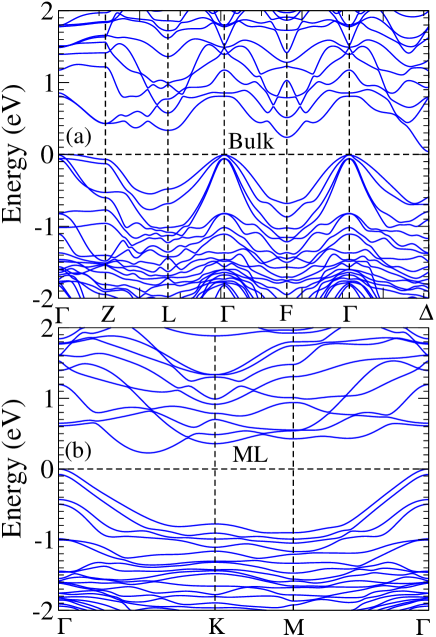
In order to understand the electronic, magnetic and optical properties of the Cr2Ge2Te6 materials, we calculate their electronic band structures. Relativistic band structures of bulk and monolayer Cr2Ge2Te6 are displayed in Fig. 3, while that of bilayer and trilayer Cr2Ge2Te6 are shown in Fig. S1 in the SM SM . It is clear from Fig. 3 and Fig. S1 that all the four structures are indirect bandgap semiconductors with the valence band maximum (VBM) being at the point. The conduction band minimum (CBM) in the Cr2Ge2Te6 multilayers is located at somewhere along the -K symmetry line (see Fig. 3 and Fig. S1) while that of bulk Cr2Ge2Te6 is located at a general -point of (0.4444, -0.3704, 0.2222). Interestingly, calculated spin-polarized scalar-relativistic band structures (see Fig. S2 in SM ), indicate that both the CBM and VBM are of purely spin-up character. The calculated bandgaps () are listed in Table I. It is seen that the theoretical bandgap of bulk Cr2Ge2Te6 is much smaller than the experimental value. This significant discrepancy between experiment and theory is due to the well-known underestimation of the bandgaps by the GGA. In order to obtain accurate optical properties which are calculated from the band structure, we also perform the band structure calculations using the hybrid Heyd-Scuseria-Ernzerhof (HSE) functional. heyd2003j ; heyd2006 The HSE band structures are displayed in Fig. S3 in the SMSM and the HSE band gaps are listed in Table I. The HSE bandgap of bulk Cr2Ge2Te6 is now comparable to the experimental value (Table I). Therefore, the optical properties of all the Cr2Ge2Te6 materials are calculated from the GGA band structures within the scissors correction schemeLevine91 using the differences between the HSE and GGA bandgaps (Table I).
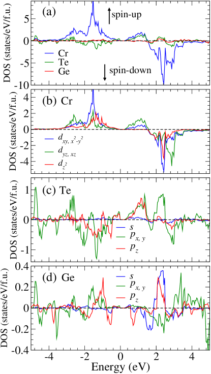
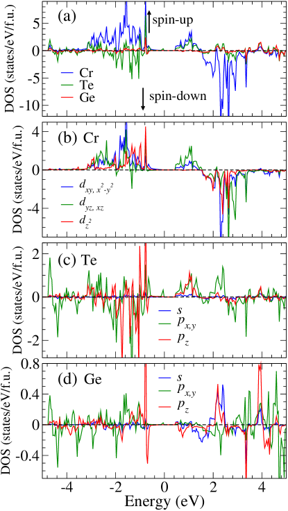
We also calculate total as well as site-, orbital-, and spin-projected densities of states (DOS) for all the Cr2Ge2Te6 materials. In Fig. 4, we display site-, orbital- and spin-projected DOSs of bulk Cr2Ge2Te6. It can be seen that the upper valence band ranging from -4.0 eV to -0.3 eV and also the lower conduction band ranging from 0.4 eV to 4.0 eV originate mainly from Cr orbitals with minor contributions from Te orbitals due to the hybridization between Cr and Te orbitals. The valence bands below these spin-up Cr -dominant bands, are primarily derived from Te orbitals. Furthermore, the upper valence band ranging from -3.3 eV to -0.3 eV consists of a broad peak of mainly spin-up Cr orbitals. The lower conduction bands ranging from 0.4 eV to 1.5 eV is mainly made up of spin-up Cr orbitals. This suggests that the bandgap is created by the crystal-field spliting of spin-up Cr and bands. Above this up to 3.6 eV, the conduction band consists of a pronounced peak of spin-down Cr and orbitals.
Site-, orbital- and spin-projected DOSs of ML Cr2Ge2Te6 are shown in Fig. 5. Clearly, the features in the DOSs spectra of the ML are rather similar to that in the DOSs spectra of bulk Cr2Ge2Te6 (Fig. 4). The main difference appears to be that the contributions from the orbitals of Te and Ge atoms are enhanced in the higher energy region. Another difference is the enhanced bandgap in the ML mainly due to the lack of interlayer interaction. Site-, orbital- and spin-projected DOSs of BL and TL Cr2Ge2Te6 fall between that of ML and bulk Cr2Ge2Te6 and thus are not shown here.
According to perturbation theory analysis, only the occupied and unoccupied Cr states near the Fermi level which are coupled by the SOC, would significantly contribute to the magneto-crystalline anisotropy. wang1993 Moreover, the SOC matrix elements and are found to prefer the out-of-plane anisotropy, while , and favor an in-plane anisotropy. Takayama The ratio of these matrix elements are :: : : = . Figures 4(b) and 5(b) show that in both bulk and ML Cr2Ge2Te6, Cr DOS is almost zero in the CBM region of 0.41.5 eV, and consequently, matrix element would be negligibly small and thus hardly contribute to the C-MAE. In contrast, Cr DOS has prominent peaks in both VBM and CBM regions, and hence matrix element would be large. This would give rise to a dominating contribution to the C-MAE. All these together would then lead to a C-MAE which prefers the out-of-plane anisotropy in the Cr2Ge2Te6 materials.
III.4 Optical conductivity
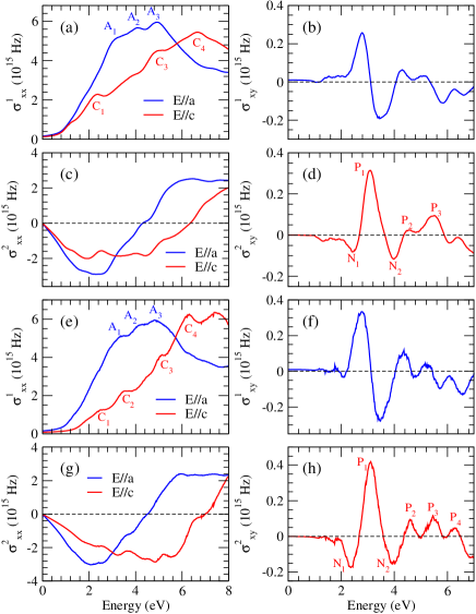
We calculate the optical conductivity tensors for all the considered Cr2Ge2Te6 materials with the scissor corrections. Calculated optical conductivity elements are displayed in Fig. 6 for bulk and ML Cr2Ge2Te6 as well as in Fig. S4 for the BL and in Fig. S5 for the TL in the SM SM . Overall, the calculated optical spectra for all the systems are rather similar (Fig. 6, Fig. S4 and Fig. S5). This could be expected from the weak interlayer interaction in layered vdW materials such as Cr2Ge2Te6. Therefore, in what follows, we will take that of bulk and ML Cr2Ge2Te6 as examples to perform detailed analysis (Fig. 6). First of all, the diagonal elements (for in-plane electric field polarization ) and (for out-of-plane polarization ) of the optical conductivity for both systems are significantly different (Fig. 6), i.e., these materials exhibit rather strong optical anisotropy. For example, the absorptive part of is much larger than in the low energy range of 1.0 5.5 eV, while it is smaller than in the energy range above 6.0 eV. This pronounced optical anisotropy could be expected from a 2D or quasi-2D material, and also can be qualitatively explained by the Cr -orbital-projected DOSs. As mentioned above, the upper valence band ranging from -4.0 to -0.3 eV is dominated by Cr -orbitals. In particular, Figs. 5(b) and 6(b) show that in this region, the overall weight of Cr is much larger than that of Cr . Given that () states can be excited by only () polarized light while Cr states can be excited by light of both polarizations, would obviously be larger than in the low energy region, as shown in Figs. 6(a) amd 6(e).
For both bulk and ML Cr2Ge2Te6, the increases steeply from the absorption edge (1.0 eV) to 3.0 eV, and then further increases up to 4.9 eV with a much smaller slope. Beyond 4.9 eV, the decreases monotonically with the energy (see Fig. 6). The also increases steadily from the absorption edge to 6.5 eV with a smaller slope, however, and then decreases as the energy further increases (Fig. 6). The and spectra from bulk and ML Cr2Ge2Te6 share several common characteristics: (a) a broad valley centered at 2.5 eV (4.0 eV) in the (), (b) a sign change in the () occurring at 4.5 eV (6.5 eV), and (c) a plateau in the above 6.0 eV [see Figs. 6(c) and 6(g)].
Figure 6 shows that both real () and imaginary () parts of the off-diagonal element of the optical conductivity of bulk and ML Cr2Ge2Te6 are also rather similar. For example, all these spectra exhibit pronounced oscillatory peaks although the peak amplitude decreases with the energy. Notably, both and show a large positive peak at 2.8 eV and 3.0 eV, respectively (Fig. 6). They also have a pronounced negative peak at 3.5 eV and 4.0 eV, respectively.
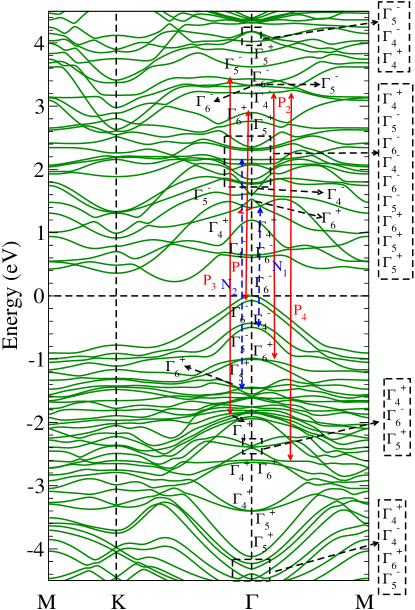
As Eqs. (4), (5) and (11) suggested, the absorptive parts of the optical conductivity elements (, , , ) are directly related to the dipole-allowed interband transitions. This would allow us to understand the origins of the main peaks in the , and spectra by determining the symmetries of the calculated band states and also the dipole selection rules. As discussed above, the features in the , and spectra for all the considered systems are rather similar. Therefore, as an example, here we perform a symmetry analysis for ML Cr2Ge2Te6 only (see the SM SM ). The found symmetries of the band states at the -point of the scalar-relativistic and relativistic band structures of ML Cr2Ge2Te6 are displayed in Fig. S6 and Fig. 7, respectively. Using the dipole selection rules (Table S3), we could assign the main peaks in the and spectra [Fig. 6(e)] to the interband transitions at the -point displayed in Fig. S6. For example, we could relate the A1 peak at 3.4 eV in [Fig. 6(e)] to the interband transition from the state at the top of the spin-down valence band to the conduction band state at 3.1 eV [Fig. S6(b)]. Of course, in addition to this, there may be contributions from different interband transitions at other -points. Note that without the SOC, the and band states are doubly degenerate (Fig. S6), and the absorption rates for left- and right-handed polarized lights are the same. When the SOC is included, these band states split (Fig. 7), and this results in magnetic circular dichroism. Therefore, we could assign the main peaks in the to the principal interband transitions at the -point only in the relativistic band structure, e. g., displayed in Fig. 7. In particular, we could attribute the pronounced peak P1 at 3.0 eV in [Fig. 6(h)] to the interband transition from the and states at the top of the valence band to the conduction band state at 2.8 eV (Fig. 7).
III.5 Magneto-optical Kerr and Faraday Effects
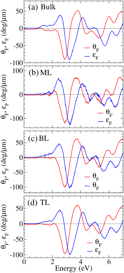
Here we consider the polar Kerr and Faraday effects for all the systems considered, and calculate their complex Kerr and Faraday rotation angles as a function of photon energy, as plotted in Figs. 8 and 9, respectively. Figure 8 shows that for the three multilayers, the spectra are negligibly small below 1.2 eV but become large and oscillatory in the incident photon energy range from 1.2 eV to 7.0 eV. In particular, the Kerr rotation angle in all the multilayers, is remarkably large in the vicinity of 2.8 eV, reaching up to 0.4∘ for the ML, 0.6∘ for the BL and 1.0∘ for the TL. The shapes of the Kerr rotation spectra for all the multilayers are similar, indicating the weakness of the vdW interlayer interaction. The Kerr rotation spectrum for the bulk is similar to that of the multilayers, except it is not negligible below 1.2 eV where bulk Cr2Ge2Te6 also shows significant Kerr rotations [see Fig. 8(a)], which will be explained below.
A comparison of Fig. 8 with Fig. 6 would reveal that the Kerr rotation () and Kerr ellipticity () spectra in all the systems resemble, respectively, the corresponding real part () and imaginary part () of the off-diagonal conductivity element. This is not surprising because the Kerr effect and the off-diagonal conductivity element are connected via Eqs. (8) and (9). Indeed, Eqs. (8) and (9) indicate that the complex Kerr rotation angle would be linearly related to the if the longitudinary conductivity () of the bulk and substrate is more or less constant. For the Cr2Ge2Te6 multilayers, the latter is true because here we assume that the substrate is SiO2 with dielectric constant . For bulk Cr2Ge2Te6, the Kerr rotation could become large if the , which is in the denominator of Eq. (8), becomes very small. This explains that the Kerr rotation of the bulk is still visible below 1.2 eV (Fig. 8).
Let us now compare the calculated Kerr rotation angles in the Cr2Ge2Te6 materials with that found in several well-known MO materials. Ferromagnetic 3 transition metals and their alloys form an important class of metallic MO materials. antonov2004 Kerr rotation angles of these metals seldom exceed 0.5∘ except a few of them such as heavy element Pt intermetallics FePt, Co2Pt guo1996 and PtMnSb van1983ptmnsb where the strong SOC in the Pt atoms plays an important role. guo1996 . Manganese pnictides also have excellent MO properties. In particar, MnBi films possess a large Kerr rotation angle of 2.3∘ at 1.84 eV in low temperatures. di1996optical ; ravindran1999 Remarkably, calculated Kerr rotation angles of bulk and few-layer Cr2Ge2Te6 (Fig. 8) are comparable to that of these traditional excellent MO materials. Furthermore, they are generally more than 10 times larger than that of FM 3 transition metal MLs deposited on metallic substrates. For example, BL Fe epitaxially grown on Au (001) surface exhibits largest Kerr rotation angle of only 0.025∘ at 2.75 eV. geerts1994 In this context, the Kerr rotation angles of atomically thin Cr2Ge2Te6 films could be regarded to be gigantic.
Among famous MO semiconductors, Y3Fe5O12 exhibits a significant Kerr rotation of 0.23∘ at 2.95 eV. tomita2006 Recently, dilute magnetic semiconductors were reported to show significant Kerr rotation angles of 0.4∘ in the vicinity of 1.80 eV. lang2005 Remarkably, Feng et. al. recently studied theoretically the MO properties of hole-doped Group-IIIA metal-monochalcogenide MLs and predicted that many of these FM MLs would exhibit significant Kerr rotations of 0.3∘ at optimal hole concentrations. feng2016 On the whole, the Kerr rotation angles predicted for bulk and few-layer Cr2Ge2Te6 here are comparable to these important MO semiconductors. Therefore, because of their excellent MO properties, Cr2Ge2Te6 materials could find promising applications for, e.g., MO sensors and high density MO data-storage devices. Moreover, MOKE in atomically thin films as well as bulk Cr2Ge2Te6 at low temperatures has been measured using highly sensitive Sagnac interferometer with light wavelength of 1550 nm (photon energy of 0.8 eV). gong2017 The measured value of 0.14∘ of the bulk is in the same order of magnitude with our theoretical prediction [see Fig. 8(a)]. The values for the thin films are, however, much smaller, ranging from 0.0007∘ in bilayer to 0.002∘ in trilayer. gong2017 Such small measured values could be attributed to the fact that the energy of light beam used falls almost within the bandgap where MOKE is negligibly small (Fig. 8). Indeed, the value of 0.28∘ of the CrI3 ML measured using a 633-nm HeNe laser (photon energy of 1.96 eV) huang2017 is orders of magnitude larger than the Cr2Ge2Te6 thin films reported in gong2017 .
Complex Faraday rotation angles for all the considered structures are displayed in Fig. 9. The Faraday rotation spectra are similar to the corresponding Kerr rotation spectra (Fig. 8) as well as the (see Fig. 6). Figure 6 shows that the is generally much larger than the . Thus, . Consequently, Eq. (10) can be approximately written as or where is the dielectric function. This explains why the complex Faraday rotation follows closely (Figs. 6 and 9).
Remarkably, calculated maximum Faraday rotation angles are as large as deg/m in 2D Cr2Ge2Te6 (see Fig. 9). In the visible frequency range (below 4.0 eV), they are more than ten times larger than the predicted Faraday rotations in Group-IIIA metal-monochalcogenide monolayers at optimal hole dopings. feng2016 They are even comparable to that of prominent bulk MO metals such as manganese pnictides. In particular, among manganese pnictides, MnBi films possess the largest Faraday rotations of deg/m at 1.77 eV at low temperatures. di1996optical ; ravindran1999 Even the famous MO semiconductor Y3Fe5O12 exhibits a Faraday rotation only as large as deg/m at 2.07 eV.boudiar2004 However, substituting Y with Bi could substantially enhance Faraday rotations up to deg/m at 2.76 eV in Bi3Fe5O12 vertruyen2008curie . Clearly, the Faraday rotation angles reported here for few-layer multilayer Cr2Ge2Te6 are comparable or even superior to many well-known MO materials. This suggests that one could also exploit the large Faraday effect to probe the long range magnetic orders in these quasi-2D magnetic materials. Furthermore, benefited from the excellent MO properties, Cr2Ge2Te6 materials could find valuable applications for magnetic-optical devices.
IV CONCLUSION
We have investigated magnetism as well as electronic, optical and magneto-optical properties of atomically thin FM films recently exfoliated from bulk FM semiconductor Cr2Ge2Te6 by performing systematic GGA+U calculations. In particular, we focus on two relativity-induced properties of these 2D materials, namely, magnetic anisotropy energy and MO effects. Firstly, we find that calculated MAEs of these materials are large, being in the order of 0.1 meV/Cr. Interestingly, the out-of-plane anisotropy is found in all the considered systems except the ML. In contrast, in the ML an in-plane magnetization is preferred simply because the D-MAE is larger than the C-MAE. Crucially, this would explain why long-range FM order was recently observed in all the few-layer Cr2Ge2Te6 except the ML. This is because the out-of-plane anisotropy would open a spin-wave gap and thus suppress magnetic fluctuations so that long-range FM order could be stabilized at finite temperature. Secondly, large Kerr rotations up to 1.0∘ in these FM materials are found in the visible frequency range, and they are comparable to that observed in famous MO materials such as FM metal PtMnSb and semiconductor Y3Fe5O12. Moreover, they are two-order of magnitude larger than that of 3 transition metal MLs deposited on Au surfaces, and thus can be called gigantic. Thirdly, calculated maximum Faraday rotation angles in these 2D materials are also large, being up to 120 deg/m, and are comparable to the best-known MO semiconductor Bi3Fe5O12. These findings thus suggest that with large MO effects plus significant MAE, atomically thin films of Cr2Ge2Te6 might find valuable applications in 2D magnetic, magneto-electric and MO device such as high-density data-storage and nanomagnetic sensors. Fourthly, calculated Kerr rotation angles at 1550 nm wavelength are in reasonable agreement with recent MO Kerr effect experiments. The FM transition temperatures estimated using the calculated exchange coupling parameters within the mean-field approximation plus the spin-wave gap correction agree quite well with the measured transition temperatures. Finally, the calculated C-MAE and MO properties of these 2D materials are analyzed in terms of their electronic band structures.
ACKNOWLEDGEMENTS
Y. F. thanks Department of Physics and Center for Theoretical Physics, National Taiwan University for its hospitality during her three months visit there when parts of this work were carried out. Work at Xiamen University is supported by the National Key Research Program of China (Grant No. 2016YFA0202601), the National Natural Science Foundation of China (No. 11574257), and the Fundamental Research Funds for the Central Universities (No. 20720180020). G. Y. G. acknowledges the support by the Ministry of Science and Technology, the Academia Sinica, the National Center for Theoretical Sciences and the Kenda Foundation of Taiwan.
References
- (1) K. S. Novoselov, A. K. Geim, S. V. Morozov, D. Jiang, Y. Zhang, S. V. Dubonos, I. V. Grigorieva and A. A. Firsov, Science 306, 666 (2004).
- (2) P. Miro, M. Audiffred and T. Heine, Chem. Soc. Rev. 43, 6537-54 (2014).
- (3) G. R. Bhimanapati, Z. Lin, V. Meunier, Y. Jung, J. Cha, S. Das, D. Xiao, Y. Son, M. S. Strano, V. R. Cooper, L. Liang, S. G. Louie, E. Ringe, W. Zhou, S. S. Kim, R. R. Naik, B. G. Sumpter, H. Terrones, F. Xia, Y. Wang, J. Zhu, D. Akinwande, N. Alem, J. A. Schuller, R. E. Schaak, M. Terrones, and J. A. Robinson, ACS Nano 9, 11509-11539 (2015).
- (4) K. F. Mak, C. Lee, J. Hone, J. Shan and T. F. Heinz, Phys. Rev. Lett. 105, 136805 (2010).
- (5) D. Xiao, G.-B. Liu, W. Feng, X. Xu and W. Yao, Phys. Rev. Lett. 108, 196802 (2012).
- (6) K.-A. Duerloo, M. T. Ong, E. J. Read, J. Phys. Chem. Lett. 3, 2871 (2012).
- (7) C.-Y. Wang and G.-Y. Guo, J. Phys. Chem. C 119, 13268 (2015).
- (8) T. Gao, Z. Li and S. G. Louie, Phys. Rev. Lett. 114, 236602 (2015).
- (9) W. Feng, G.-Y. Guo, and Y. Yao, 2D Mater. 4, 015017 (2016).
- (10) C.-S. Tan, Y.-J. Lu, C.-C. Chen, P.-H. Liu, S. J. Gwo, G.-Y. Guo and L.-J. Chen, J. Phys. Chem. C 120, 23055 (2016).
- (11) X. Li and J. Yang, J. Mater. Chem. C 2, 7071-7076 (2014).
- (12) W.-B. Zhang, Q. Qu, P. Zhu and C.-H. Lam, J. Mater. Chem. C 3, 12457-12468 (2015)
- (13) N. Sivadas, M. W. Daniels, R. H. Swendsen, S. Okamoto, and D. Xiao, Phys. Rev. B 91, 235425 (2015).
- (14) M.-W. Lin, et al. J. Mater. Chem. C 4, 315-322 (2016).
- (15) B. Huang, G. Clark, E. Navarro-Moratalla, D. R. Klein, R. Cheng, K. L. Seyler, D. Zhong, E. Schmidgall, M. A. McGuire, D. H. Cobden, W. Yao, D. Xiao, P. Jarillo-Herrero, X. Xu, Nature 546, 270–273 (2017).
- (16) C. Gong, L. Li, Z. Li, H. Ji, A. Stern, Y. Xia, T. Cao, W. Bao, C. Wang, Y. Wang, Z. Q. Qiu, R. J. Cava, S. G. Louie, J. Xia and X. Zhang, Nature 546, 265 (2017).
- (17) V. Carteaux, D. Brunet, G. Ouvrard, and G. Andre, J. Phys.: Condens. Matter 7, 69 (1995).
- (18) X. Zhang, Y. Zhao, Q. Song, S. Jia, J. Shi, and W. Han, Jpn. J. Appl. Phys. 55, 033001 (2016).
- (19) H. Ji, R. Stokes, L. Alegria, E. Blomberg, M. Tanatar, A. Reijnders, L. Schoop, T. Liang, R. Prozorov, K. Burch, et al., J. Appl. Phys. 114, 114907 (2013).
- (20) N. D. Mermin and H. Wagner, Phys. Rev. Lett. 17, 1133 (1966).
- (21) G. Y. Guo, W. Temmerman, and H. Ebert, J. Phys.: Condens. Matter 3, 8205 (1991).
- (22) J. C. Tung and G. Y. Guo, Phys. Rev. B 76, 094413 (2007).
- (23) Y. Tian, M. J. Gray, H. Ji, R. Cava, and K. S. Burch, 2D Mater. 3, 025035 (2016).
- (24) W. Xing, Y. Chen, P. M. Odenthal, X. Zhang, W. Yuan, T. Su, Q. Song, T. Wang, J. Zhong, S. Jia, X. C. Xie, Y. Li and W. Han, 2D Mater. 4, 024009 (2017).
- (25) P. M. Oppeneer, Chapter 1 Magneto-optical Kerr Spectra, pp. 229-422, in Handbook of Magnetic Materials, edited by K. H. J. Buschow. Elsevier, Amsterdam, (2001).
- (26) V. Antonov, B. Harmon, and A. Yaresko. Electronic structure and magneto-optical properties of solids. Springer Science & Business Media, (2004).
- (27) M. Mansuripur, The Principles of Magneto-Optical Recording (Cambridge Univ. Press, Cambridge, 1995).
- (28) J. P. Castera, in Magneto-optical Devices, Vol. 9 of Encyclopedia of Applied Physics, edited by G. L. Trigg (Wiley-VCH, New York, 1996), p. 133.
- (29) J. P. Perdew, K. Burke, and M. Ernzerhof, Phys. Rev. Lett. 77, 3865 (1996).
- (30) S. L. Dudarev, G. A. Botton, S. Y. Savrasov, C. J. Humphreys and A. P. Sutton, Phys. Rev. B 57, 1505 (1998).
- (31) See Supplemental Materials at http://link.aps.org/supplemental/ for Table S1 and Figs. S1-S6, which includes Ref. zhang2016, .
- (32) G. Kresse and D. Joubert, Phys. Rev. B 59, 1758 (1999).
- (33) G. Kresse and J. Furthmüller, Phys. Rev. B 54, 11169 (1996).
- (34) G. Kresse and J. Furthmüller, Comput. Mat. Sci 6, 15 (1996).
- (35) K. Lee, E. D. Murray, L. Kong, B. I. Lundqvist and D. C. Langreth, Phys. Rev. B 82, 081101 (2010).
- (36) P. Ewald, Ann. Phys. 64, 253 (1921).
- (37) C. S. Wang and J. Callaway, Phys. Rev. B 9, 4897 (1974).
- (38) P. M. Oppeneer, T. Maurer, J. Sticht and J. Kübler, Phys. Rev. B 45, 10924 (1992).
- (39) W. Feng, G.-Y. Guo, J. Zhou, Y. Yao, and Q. Niu, Phys. Rev. B 92, 144426 (2015).
- (40) B. Adolph, J. Furthmüller and F. Bechstedt, Phys. Rev. B 63, 125108 (2001).
- (41) W. M. Temmerman, P. A. Sterne, G. Y. Guo and Z. Szotek, Molecular Simulations 63, 153 (1989).
- (42) G. Y. Guo, K. C. Chu, D.-s. Wang and C.-g. Wang, Phys. Rev. B 69, 205416 (2004).
- (43) D. Y. Qiu, F. H. da Jornada, and S. G. Louie, Phys. Rev. Lett. 111, 216805 (2013).
- (44) H. C. Hsueh, G. Y. Guo and S. G. Louie, Phys. Rev. B 84, 085404 (2011).
- (45) J. Heyd, J. Chem. Phys. 118, 8207 (2003).
- (46) J. Heyd, G. E. Scuseria, and M. Ernzerhof, J. Chem. Phys. 124, 219906 (2006).
- (47) L. X. Benedict, E. L. Shirley and R. B. Bohn, Phys. Rev. B. 57, 9385(R) (1998).
- (48) A. Budweg, D. Yadav, A. Grupp, A. Leitenstorfer, M. Trushin, F. Pauly and D. Brida, arXiv: 1712.06330v1 (2017).
- (49) G. Y. Guo and H. Ebert, Phys. Rev. B 50, 10377 (1994).
- (50) G. Y. Guo and H. Ebert, Phys. Rev. B 51, 12633 (1995).
- (51) Y. Suzuki, T. Katayama, S. Yoshida, K. Tanaka, and K. Sato, Phys. Rev. Lett. 68, 3355 (1992).
- (52) P. Ravindran, A. Delin, P. James, B. Johansson, J. Wills, R. Ahuja, and O. Eriksson, Phys. Rev. B 59, 15680 (1999).
- (53) G. Y. Guo, W. Temmerman, and H. Ebert, Physica B 172, 61-69 (1991).
- (54) P. M. Oppeneer, J. Magn. Magn. Mater. 188, 275 (1998).
- (55) S. V. Halilov, H. Eschrig, A. Y. Perlov and P. M. Oppeneer, Phys. Rev. B 58, 293 (1998).
- (56) S. V. Halilov, A. Y. Perlov and P. M. Oppeneer and H. Eschrig, Europhys. Lett. 39, 91 (1997).
- (57) M. Pajda, J. Kudrnovsky, I. Turek, V. Drchal and P. Bruno, Phys. Rev. Lett. 85, 5424 (2000).
- (58) V. Y. Irkhin, A. A. Katanin and M. I. Katsnelson, Phys. Rev. B 60, 1082 (1999).
- (59) Z. H. Levine and D. C. Allan, Phys. Rev. B 43, 4187 (1991).
- (60) D.-S. Wang, R. Wu and A. J. Freeman, Phys. Rev. B 47, 14932 (1993).
- (61) H. Takayama, K.-P. Bohnen and P. Fulde, Phys. Rev. B 14, 3387 (1976).
- (62) G. Y. Guo and H. Ebert, J. Magn. Magn. Mater. 156, 173 (1996).
- (63) P. Van Engen, K. Buschow, R. Jongebreur, and M. Erman, Appl. Phys. Lett. 42, 202–204 (1983).
- (64) G. Di and S. Uchiyama, Phys. Rev. B 53, 3327 (1996).
- (65) W. Geerts, Y. Suzuki, T. Katayama, K. Tanaka, K. Ando and S. Yoshida, Phys. Rev. B 50, 12581 (1994).
- (66) S. Tomita, T. Kato, S. Tsunashima, S. Iwata, M. Fujii and S. Hayashi, Phys. Rev. B 96, 167402 (2006)
- (67) R. Lang, W. H. Pascher, H. Krenn, X. Liu and J. K. Furdyna, Phys. Rev. B 72, 024430 (2005).
- (68) T. Boudiar, B. Payet-Gervy, M.-F. Blanc-Mignon, J.-J. Rousseau, M. Le Berre and H. Joisten, J. Magn. Magn. Mater. 284, 77-85 (2004).
- (69) B. Vertruyen, R. Cloots, J. Abell, T. Jackson, R. Da Silva, E. Popova, and N. Keller, Phys. Rev. B 78, 094429 (2008).