La-Doped BaSnO3 Electron Transport Layer for Perovskite Solar Cells
Abstract
Due to the photo-instability and hysteresis of TiO2 electron transport layer (ETL) in perovskite solar cells (PSCs), novel electron transport materials are highly demanded. Here, we show ideal band alignment between La-doped BaSnO3 (LBSO) and methyl ammonium (MA) lead iodide perovskite (MAPbI3). The CH3NH3PbI3/LaxBa(1-x)SnO3 interface forms a stable all-perovskite heterostructure. The selective band alignment is manipulated with band gap renormalization by La-doping on the Ba site. LBSO shows high mobility, photo-stability, and structural stability, promising the next generation ETL materials.
Solar energy is a highly efficient and eco-friendly source for the future energy harvesting. In recent years, PSCs based on inorganic/organic hybrid halide ABX3 (A = Cs+, CH3NH (MA), CHN2H (FA); B = Pb2+; X = Cl-, Br- or I-) have shown a rapid progress to achieve over 20 Jeon et al. (2018); Yang et al. (2017) solar cell efficiency, which is considered to be most promising large-scale thin-film solar energy materialsPark et al. (2016). PSC owns many interesting physical properties including giant dielectric screeningJuarez-Perez et al. (2014), bottleneck of hot phonon relaxation processFu et al. (2017), free excitonic stateYarita et al. (2017), defect tolerancePark et al. (2018); Kim et al. (2014), and polaron stateMyung et al. (2018a) with an ideal band gap, mobility, and optical absorbance.
TiO2 has been the most popular ETL material for PSC devices. Both anatase and rutile TiO2 have achieved high power conversion efficiency (PCE)Jeon et al. (2018); Liu et al. (2018). However, the ultraviolet-induced photocatalysis of TiO2 shows device degradation and gradual performance deterioration over a long exposureLeijtens et al. (2013). Direct optical measurements have shown that electron barrier of 0.1 eV may exist at the interface of TiO2/MAPbI3Xing et al. (2015), and such a large electron barrier causes I-V hysteresis possibly due to accumulation of iodine defects at TiO2/MAPbI3Jiang et al. (2016); Correa Baena et al. (2015); Meloni et al. (2016). To overcome these obstacles, a development for an efficient and stable next generation ETL materials is recently emergingAssadi et al. (2018). Up to date, the metal oxide materials such as SnO2, ZnO, WO3, ZnSnO4 etc. are being spotlighted as the next generation ETLMahmood et al. (2017). In a recent experiment, a new synthetic method for LBSO below 500 ∘C was developed; photostable 5 mol LBSO as ETL achieved PCE over 22 with 1000 hours illuminationShin et al. (2017).
BaSnO3 (BSO) is known as a wide indirect band gap ( 3.1 eV) materialLee et al. (2017); Kim et al. (2012) with high electrical mobilityKim et al. (2012) 300 cm2Vs-1 with possible existence of polaron state. Recent measurement of BSO thin filmPrakash et al. (2017) has achieved the room temperature conductivity over 104 Scm-1. The band gap () of BSO is easily tunable via chemical substitution with Pb, Bi or LaLee et al. (2017). As proved by the hard X-ray photoelectron spectroscopy experimentLebens-Higgins et al. (2016), this band gap tuning could be explained by the band gap renormalization due to an electrostatic interaction between the dopant cation (La3+) and extra free electrons in the conduction bandBerggren and Sernelius (1981). Therefore, rather than tuning the band gap of PSCs by A-site cation or halides substitutions, one can directly tune the band gap of ETL using BSO to achieve the optimal band alignment. We show that this scenario is also plausible at the interface of LBSO slab evidenced by a large energy difference 2-4 eV between the conduction band (Sn, O-s states) and La states (d states), which is consistent with the bulk LBSO case proven by X-ray absorption spectroscopy measurementLebens-Higgins et al. (2016).
In this work, using the density functional theory (DFT), we unveil that La doping on BSO is the key factor for the optimal band alignment at the LBSO/MAPbI3 interface. We found that though the terminations of both MAPbI3 and LBSO can affect the band alignment, the hybridization between two layers removes the dependency on the terminations. We also found that the calculated binding energies between LBSO and PSCs with various terminations are large enough to stabilize the interface.
We used Vienna Ab initio Simulation Package (VASP)Kresse and Furthmuller (1996) for non-collinear DFT calculations using PBE0 functional plus D3 van der Waals correctionGrimme et al. (2010) with inclusion of the dipole correction and the spin-orbit coupling (SOC) by switching off any presumed symmetry. We have employed the electrostatic potential of the solid to define the common vacuum level and to relate the calculation of PBE+SOC+D3 to that of PBE0+SOC+D3 which includes the Hartree-Fock exchange. The reference electrostatic local potential only includes the Hartree potential so that it is independent of the exchange-correlation functionals we choose Walle and Martin (1987); Conesa (2012) (see the Supplemental Material).
We employed a symmetric slab for BSO and MAPbI3 slabs. A supercell consists of 3 BSO layers (BaO-terminated and SnO2-terminated) and 3 layers of cubic MAPbI3 layers (MAI-terminated and PbI2-terminated) with (001) orientation for both, where the lattice mismatch using BSO(001)- and MAPbI3(001)- is as small as 1.0 . A vacuum size of 30 is included.

We first investigate the electronic structures of bulk cubic MAPbI3 (Fig. 1(a)) and cubic BaSnO3 (Fig. 1(b)) perovskites using PBE0+SOC+D3 functional which correctly describes the experimental band gaps of MAPbI3 (1.5–1.6 eV)Leguy et al. (2016) and BSO (3.1-3.5 eV)Lee et al. (2017). Indeed, our calculation shows that PBE0+SOC+D3 is the optimal choice, Eg,PBE0+SOC+D3(MAPbI3) = 1.59 eV (Fig. 1(a)) and Eg,PBE0+SOC+D3(BSO) = 3.51 eV (Fig. 1(b)). We find HSE06+SOC+D3 functional underestimates the experimental band gap for both materials, Eg,HSE06+SOC+D3(MAPbI3) = 1.03 eV and Eg,HSE06+SOC+D3(BSO) = 2.79 eV. We also find that BSO’s band gap is susceptible to the lattice constant (BSO). Thus, we have used (BSO) = 4.09 to match the experimental band gap. In contrast to MAPbI3 in which the conduction and valence energy levels significantly shift, such shifts in BSO are almost negligible with the inclusion of SOC, = 40 meV. In BSO, the conduction band minimum (CBM) is the bonding state between Sn -orbital and O -orbitals at of Brillouin zone (BZ). VBM is the anti-bonding state of O -orbitals at R of BZ (Fig. 1(b)). For MAPbI3, The CBM states are and bonding states of Pb -orbital and I -orbital and the VBM state is anti-bonding state of I -orbital and Pb -orbital (Fig. 1(a)).
The band level shift is only desirable in the conduction band, unless an elevated valence band level would allow hole carriers to transport and recombine with electron carriers in ETL materials. Indeed, we note that La-doping on BSO shifts the conduction band energy down, leaving the valence band energy intact (Fig. 1(c)). Upon La-doping (), the band gap of LBSO decreases such as eV eV eV2.55 eV) due to the electrostatic interaction between La3+ dopant and the electrons in the conduction band (Fig. 1(d))Lee et al. (2017); Kim et al. (2012); Lebens-Higgins et al. (2016).
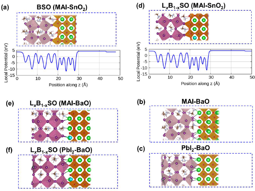
We studied various interfacial terminations between LBSO and MAPbI3. Because the work function, band gap, and band alignment are significantly affected by the slab terminations, the study of various terminations are imperative for the thorough understanding of the interface. For MAPbI3, experiments and DFT studies showed that MAI termination is thermodynamically more stable than PbI2 terminationQuarti et al. (2017). However, in PbI2-rich condition PbI2-terminated MAPbI3 surface can also be formedHaruyama et al. (2014). Previous DFT study revealed that the work function of MAI termination is 1 eV smaller than that of PbI2 termination, indicating that the termination of MAPbI3 slab plays a crucial role in determining the work function and its band alignmentQuarti et al. (2017). Along (001), the interface between BSO and MAPbI3 has four possible morphologies: MAI-terminated MAPbI3 and SnO2-terminated BSO (MAI-SnO2) (Fig. 2(a)), MAI-terminated MAPbI3 and SnO2-terminated BSO (MAI-SnO2) (Fig. 2(b)), PbI2-terminated MAPbI3 and BaO-terminated BSO (PbI2-BaO) (Fig. 2(c)) and PbI2-terminated MAPbI3 and SnO2-terminated BSO (PbI2-SnO2) (see the Supplemental Material). We investigated the minimum energy configurations of the interfaces and corresponding binding energies Eb. For the PbI2-SnO2 interface, the interfacial PbI2 (in perovskite form) becomes unstable and forms PbO2 with oxygen anions of SnO2 termination (see the Supplemental Material). Thus, at the PbI2-SnO2 interface of LBSO/MAPbI3, the perovskite forms of both materials are to be deformed into plumbic oxide. We find that this instability persists when La is doped on BSO (see the Supplemental Material). Apart from PbI2-SnO2 interface, the binding energies per unit cell of MAPbI3/LBSO for all interfaces are strong (PbI2-BaO) = 4.38 eV/unit-cell, (MAI-BaO) = 5.15 eV/unit-cell, and (MAI-SnO2) = 4.49 eV/unit-cell, larger than that of PbI2- and MAI-terminated MAPbI3/TiO2 interfaceJavaid et al. (2018). The large binding energy indicates a strong hybridization among the interfacial atoms. Therefore, we expect that the interactions between two interfaces could significantly alter the individual electronic structures.
For MAI-terminations, the interaction between NH3 of MA+ and oxygen anion depends on the termination type of LBSO. At the SnO2-termination, the short strong hydrogen bonding (SSHB)Cleland and Kreevoy (1994); Kim et al. (2000) between NH3 and O, where the hydrogen bounces back and forth between adjacent atoms, is present (see the Supplemental Material). This is rather an expected phenomenon as SSHB is also found at MAPbI3/TiO2 interface.Myung et al. (2018b) The presence of such strong hydrogen bonding (HB) is crucial because it can further stabilize the interface and can affect the energy levels between the interfaces.Myung et al. (2018b) At the BaO-termination, we observe a proton transfer from NH3 to oxygen anion (see the Supplemental Material). We find that a slight La doping () on BSO hardly affects the optimized geometry (Fig. 2). The optimized geometries for the further doping () are almost the same (see the Supplemental Material).
Depending on the terminations of MAPbI3 and BSO (PbI2, MAI, SnO2 and BaO), the work function of the system would vary significantly. This dependency on the interfacial morphology could then impact the practical performance of PSCs. However, the strong hybridizations between adjacent interfaces rearrange the pristine electronic density and so the expected large dependency on the terminations is removed (see the Supplemental Material). From the density of states (DOS) of LBSO/MAPbI3 at PBE level, we observe a sizable hybridization of interfacial atoms irrespective of the termination types (see the Supplemental Material). We also note that these hybridizations are formed between ions from the conduction and valence states (i.e. Sn and I states) without impacting the relative conduction and valence levels of adjacent layers. Thus, the scenario such as the energy level shift by the induced dipole or the charge transfer will not be the dominant factor to describe the energy levels of LBSO/MAPbI3 partly because of its role in compensating the two levels’ difference and partly because of the sizable hybridization. Even though the calculation of the charge transfer is rather easy, we are not able to get the correct physics because the PBE energy levels are not accurate enough. An accurate calculation of the charge transfer is only possible using the PBE0+SOC+D3 calculation of the whole system, which is very demanding even for the supercomputers.
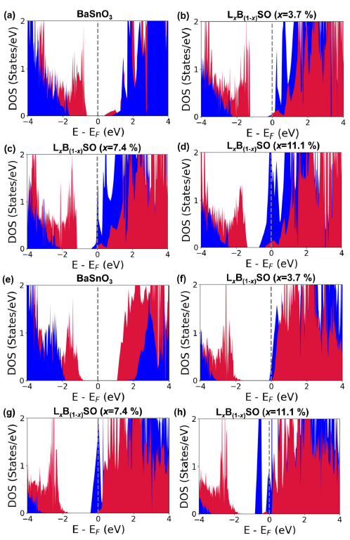
Given that the hybridization is strong in MAPbI3/LBSO, it is crucial to check if this affects the electronic states of La and the conduction band minimum (Sn , O states). For instance, if there exists a hybridization between two states, it would result in a significant modification on the conduction band’s character and its energy levels. If this is true, then the assumed mechanism on the band gap renormalization would be incorrect. To confirm the mechanism in which the Coulomb interactions between La3+ dopant and free electrons in the conduction band lowers the band edge energy, we checked the partial density of states (PDOS) of La in the slab (see the Supplemental Material). The mechanism in the bulk had been verified already in a previous studyLebens-Higgins et al. (2016). We observe that regardless of the termination types, La states do not hybridize with Sn and O states at the interface. La states are 4 eV above and 2 eV above the CBM of LBSO at , for SnO2- and BaO-terminated cases, respectively (see the Supplemental Material). This is consistent at other La concentrations. Even for an extreme case where La dopant is at the very surface of LBSO slab, we observe no hybridization between La and Sn states. Therefore, we conclude that even though the hybridization between MAPbI3 and LBSO exists, it does not affect La state, excluding a possibility of the hybridization with the conduction band.
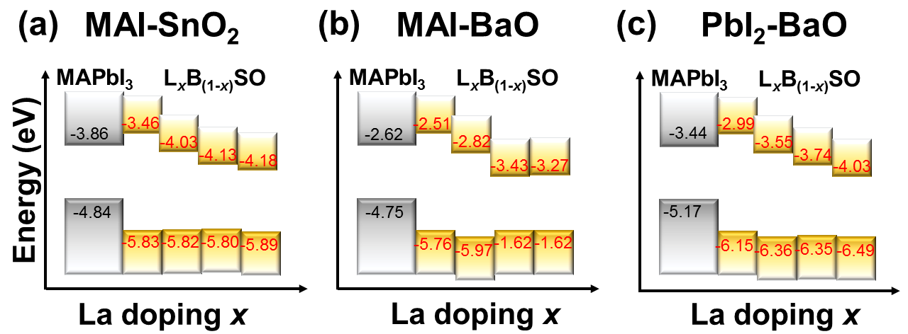
To account for the energy levels at the LBSO/MAPbI3 interface, we corrected PBE energy levels with PBE0 functional and its corrections are listed in the Supplemental Material. Without La doping, sizable electron barriers exist in all the three cases, 0.4 eV (MAI-SnO2), 0.1 eV (MAI-BaO), and 0.45 eV (PbI2-BaO), indicating that a pristine BSO would lose the open circuit voltage (Voc) and so it is not an ideal ETL for MAPbI3 (Fig 3(a) and 3(e)). To investigate the effect of La doping () on the LBSO/MAPbI3 interface, we present the results of MAI-SnO2 (Fig. 3a-c) and PbI2-BaO (Fig. 3(d)-(f)) terminated interfaces. The MAI-BaO case can be found in the Supplemental Material. Upon La-doping , only the conduction band level of LBSO shifts down (Fig. 3(b) and 3(f)) and the band alignment between MAPbI3 and LBSO starts to be favorable (or LBSO conduction band level becomes lower than MAPbI3 conduction band level) for the electron transfer process. The energy shift is more pronounced for the further La-doping and (Fig. 3(c)-(d) and 3(g)-(h)).
For all the three interfaces, the band alignments of band edge states with respect to La-doping concentrations x () are summarized in Fig. 4. For comparison, we have set the vacuum level of the system to 0 eV. In all the cases, an unfavorable conduction band alignment between MAPbI3 and BSO can be overcome by a small amount of La doping. Therefore, as a function of La-doping , one would find the optimal band alignment between MAPbI3 and LBSO to maximize VOC and corresponding PCE of the device. Therefore, a further experimental work would be required to investigate the optimal La-doping range for the maximum photovoltaic efficiency in PSCs.
In summary, we investigated the interface between a novel ETL material La-doped BaSnO3 and the cubic MAPbI3 PSCs using DFT with PBE0+SOC+D3. We found that the (001) LBSO/MAPbI3 forms stable ”all-perovskite” interfaces with large binding energy. Depending on the termination types, MA and O at the interface show SSHB and the proton transfer. Because LBSO can tune the conduction band energy selectively via La-doping due to the conduction band renormalization, it enables the control of band level solely by La-doping without halide or organic cation substitutions in PSC materials. This demonstrates an advantage of LBSO over other ETL materials in addition to the appreciated photostability over UV lights. We expect that the development of a novel ETL materials including LBSO would enable a further enhancement of the efficiency and the stability of the lead-halide-based PSC devices.
Acknowledgements.
We thank Prof. S.-.I Seok and M.-J. Paik for their valuable discussions. C.W.M. conceived the idea, performed DFT calculation, and wrote the manuscript. All discussed the calculation results. K.S.K. revised the manuscript. This work was supported by National Honor Scientist Program (2010-0020414) and Basic Science Research Program (2015R1C1A1A01055922) of NRF. Computation was supported by KISTI (KSC-2017-S1-0025, KSC-2017-C3-0081).References
- Jeon et al. (2018) N. J. Jeon, H. Na, E. H. Jung, T. Y. Yang, Y. G. Lee, G. Kim, H. W. Shin, S. Il Seok, J. Lee, and J. Seo, Nature Energy 3, 1 (2018).
- Yang et al. (2017) W. S. Yang, B.-w. Park, E. H. Jung, N. J. Jeon, Y. C. Kim, D. U. Lee, S. S. Shin, J. Seo, E. K. Kim, J. H. Noh, and S. I. Seok, 1379, 1376 (2017).
- Park et al. (2016) N.-G. Park, M. Grätzel, T. Miyasaka, K. Zhu, and K. Emery, Nature Energy 1, 16152 (2016).
- Juarez-Perez et al. (2014) E. J. Juarez-Perez, R. S. Sanchez, L. Badia, G. Garcia-Belmonte, Y. S. Kang, I. Mora-Sero, and J. Bisquert, Journal of Physical Chemistry Letters 5, 2390 (2014).
- Fu et al. (2017) J. Fu, Q. Xu, G. Han, B. Wu, C. H. A. Huan, M. L. Leek, and T. C. Sum, Nature Communications 8 (2017).
- Yarita et al. (2017) N. Yarita, H. Tahara, T. Ihara, T. Kawawaki, R. Sato, M. Saruyama, T. Teranishi, and Y. Kanemitsu, Journal of Physical Chemistry Letters 8, 1413 (2017).
- Park et al. (2018) J. S. Park, S. Kim, Z. Xie, and A. Walsh, Nature Reviews Materials 3, 194 (2018).
- Kim et al. (2014) J. Kim, S. H. Lee, J. H. Lee, and K. H. Hong, Journal of Physical Chemistry Letters 5, 1312 (2014).
- Myung et al. (2018a) C. W. Myung, J. Yun, G. Lee, and K. S. Kim, Advanced Energy Materials 8, 1 (2018a), 1711.08938 .
- Liu et al. (2018) X. Liu, Z. Liu, B. Sun, X. Tan, H. Ye, Y. Tu, T. Shi, Z. Tang, and G. Liao, Nano Energy 50, 201 (2018).
- Leijtens et al. (2013) T. Leijtens, G. E. Eperon, S. Pathak, A. Abate, M. M. Lee, and H. J. Snaith, Nature Communications 4, 1 (2013).
- Xing et al. (2015) G. Xing, B. Wu, S. Chen, J. Chua, N. Yantara, S. Mhaisalkar, N. Mathews, and T. C. Sum, Small 11, 3606 (2015).
- Jiang et al. (2016) Q. Jiang, L. Zhang, H. Wang, X. Yang, J. Meng, H. Liu, Z. Yin, J. Wu, X. Zhang, and J. You, Nature Energy 2, 16177 (2016).
- Correa Baena et al. (2015) J. P. Correa Baena, L. Steier, W. Tress, M. Saliba, S. Neutzner, T. Matsui, F. Giordano, T. J. Jacobsson, A. R. Srimath Kandada, S. M. Zakeeruddin, A. Petrozza, A. Abate, M. K. Nazeeruddin, M. Grätzel, and A. Hagfeldt, Energy Environ. Sci. 8, 2928 (2015).
- Meloni et al. (2016) S. Meloni, T. Moehl, W. Tress, M. Franckeviius, M. Saliba, Y. H. Lee, P. Gao, M. K. Nazeeruddin, S. M. Zakeeruddin, U. Rothlisberger, and M. Graetzel, Nature Communications 7 (2016).
- Assadi et al. (2018) M. K. Assadi, S. Bakhoda, R. Saidur, and H. Hanaei, Renewable and Sustainable Energy Reviews 81, 2812 (2018).
- Mahmood et al. (2017) K. Mahmood, S. Sarwar, and M. T. Mehran, RSC Adv. 7, 17044 (2017).
- Shin et al. (2017) S. S. Shin, E. J. Yeom, W. S. Yang, S. Hur, M. G. Kim, J. Im, J. Seo, J. H. Noh, and S. I. Seok, Science 356, 167 (2017).
- Lee et al. (2017) S. Lee, H. Wang, P. Gopal, J. Shin, H. M. Jaim, X. Zhang, S. Y. Jeong, D. Usanmaz, S. Curtarolo, M. Fornari, M. Buongiorno Nardelli, and I. Takeuchi, Chemistry of Materials 29, 9378 (2017).
- Kim et al. (2012) H. J. Kim, U. Kim, T. H. Kim, J. Kim, H. M. Kim, B. G. Jeon, W. J. Lee, H. S. Mun, K. T. Hong, J. Yu, K. Char, and K. H. Kim, Physical Review B - Condensed Matter and Materials Physics 86, 1 (2012).
- Prakash et al. (2017) A. Prakash, P. Xu, A. Faghaninia, S. Shukla, J. W. Ager, C. S. Lo, and B. Jalan, Nature Communications 8, 15167 (2017).
- Lebens-Higgins et al. (2016) Z. Lebens-Higgins, D. O. Scanlon, H. Paik, S. Sallis, Y. Nie, M. Uchida, N. F. Quackenbush, M. J. Wahila, G. E. Sterbinsky, D. A. Arena, J. C. Woicik, D. G. Schlom, and L. F. Piper, Physical Review Letters 116, 1 (2016).
- Berggren and Sernelius (1981) K. F. Berggren and B. E. Sernelius, Physical Review B 24, 1971 (1981).
- Kresse and Furthmuller (1996) G. Kresse and J. Furthmuller, Comput. Mater. Sci. 6, 15 (1996).
- Grimme et al. (2010) S. Grimme, J. Antony, S. Ehrlich, and H. Krieg, Journal of Chemical Physics 132 (2010).
- Walle and Martin (1987) C. D. Walle and R. Martin, Physical Review B 35, 8154 (1987).
- Conesa (2012) J. C. Conesa, The Journal of Physical Chemistry C 116, 18884 (2012).
- Leguy et al. (2016) A. M. A. Leguy, P. Azarhoosh, M. I. Alonso, M. Campoy-Quiles, O. J. Weber, J. Yao, D. Bryant, M. T. Weller, J. Nelson, A. Walsh, M. van Schilfgaarde, and P. R. F. Barnes, Nanoscale 8, 6317 (2016).
- Quarti et al. (2017) C. Quarti, F. De Angelis, and D. Beljonne, Chemistry of Materials 29, 958 (2017).
- Haruyama et al. (2014) J. Haruyama, K. Sodeyama, L. Han, and Y. Tateyama, The Journal of Physical Chemistry Letters 5, 2903 (2014).
- Javaid et al. (2018) S. Javaid, C. W. Myung, J. Yun, G. Lee, and K. S. Kim, Journal of Materials Chemistry A 6, 4305 (2018).
- Cleland and Kreevoy (1994) W. W. Cleland and M. M. Kreevoy, Science (New York, N.Y.) 264, 1887 (1994).
- Kim et al. (2000) K. S. Kim, K. S. Oh, and J. Y. Lee, Proceedings of the National Academy of Sciences of the United States of America 97, 6373 (2000).
- Myung et al. (2018b) C. W. Myung, S. Javaid, K. S. Kim, and G. Lee, ACS Energy Letters 3, 1294 (2018b), 1801.05531 .