Current address: ]Division of National Supercomputing Research and Development, Korea Institute of Science and Technology Information (KISTI), 245 Daehak-ro, Yuseong-gu, Daejeon 34141, Republic of Korea
Constrained-search density functional study of quantum transport in two-dimensional vertical heterostructures
Abstract
Based on a microcanonical picture that maps the steady-state quantum transport process to a drain-to-source excitation, we develop a constrained-search density functional formalism for finite-bias quantum transport calculations. By variationally minimizing the total energy of an electrode-channel-electrode system without introducing separate bulk electrode information, ambiguities in identifying its nonequilibrium electronic structure under a bias is reduced and finite electrode cases can be naturally treated. We apply the approach to vertically stacked van der Waals heterostructures made of a hexagonal boron nitride (hBN) channel sandwiched by single-layer graphene electrodes, which so far could not be treated within first-principles calculations. We find that the experimentally observed negative differential resistance originates from the hBN defect-mediated hybridizations between two graphene states, and concurrently obtain a high-bias linear current increase that was not captured in previous semiclassical treatments. Going beyond the capability of existing ab initio nonequilibrium quantum transport simulation methods, the developed formalism will provide valuable atomistic information in the development of next-generation nanodevices.
- Subject Areas
-
Quantum transport Constrained-search density functional theory Graphene Vertical transistor Negative differential resistance
I Introduction
Density functional theory (DFT) in the standard form cannot be applied to nonequilibrium quantum electron transport phenomena, thus in the last decade or so the DFT-based nonequilibrium Green’s function (NEGF) formalism has been established as the standard approach for first-principles quantum transport calculations Datta2005 ; DiVentra2008 . While successful, the DFT-NEGF approach suffers from several shortcomings due the the Landauer picture invoked in its practical realization. The device is viewed within the Landauer picture as an open system with an external battery as the source of the current flow, and to implement this viewpoint one replaces the Hamiltonian and related matrix elements corresponding to the semi-infinite electrode regions with those from separate infinite bulk calculations.
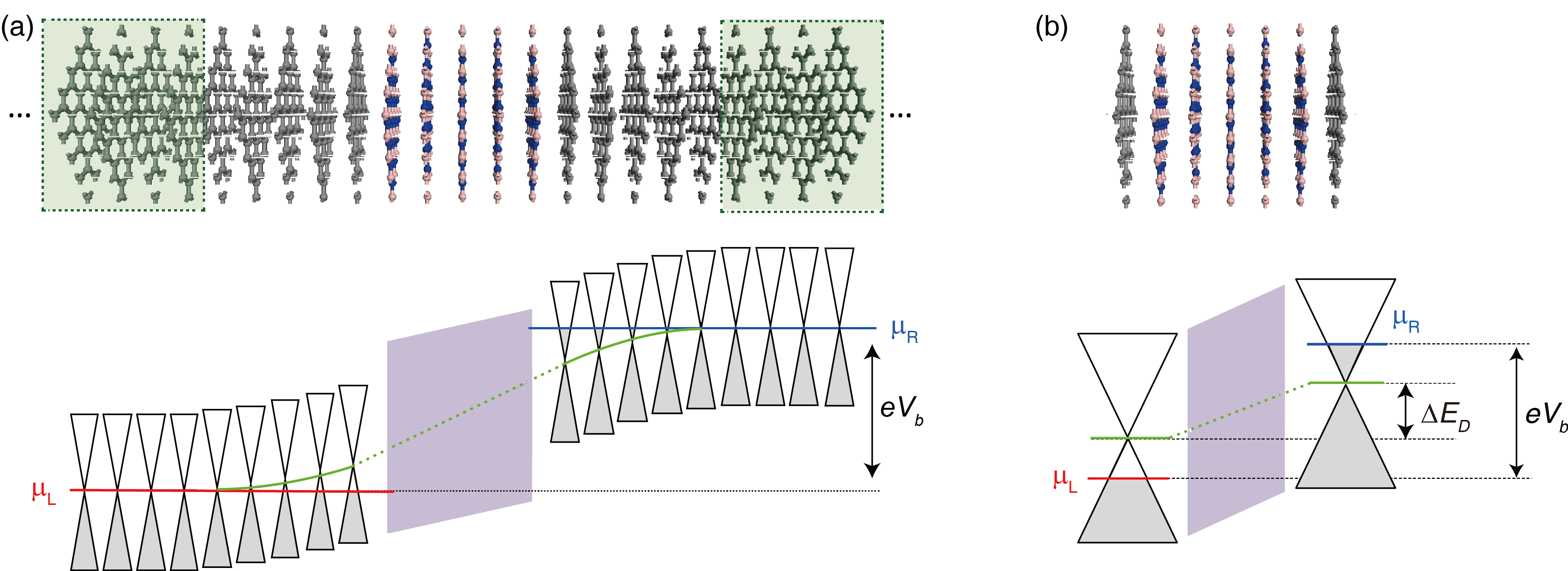
So, DFT-NEGF requires the electrodes to be repeated semi-infinitely, making junction models based on finite-dimension electrodes intrinsically non-tractable. This unfortunately implies that the recently developed transistors constructed by vertically stacking two-dimensional (2D) semiconductor materials and single-layer graphene electrodes Britnell2012_SC ; Britnell2013 ; Jena2013 ; Li2016 ; Iannaccone2018 cannot be treated within DFT-NEGF.
Due to the fundamental limitation of the DFT-NEGF method, simulations of transistors based on 2D heterostructures are currently performed by replacing single-layer graphene (Fig. 1A) with infinite-layer graphite electrodes (Fig. 1B) or resorting to semi-classical approaches such as the Bardeen transfer Hamiltonian formalism. Both directions are clearly undesirable in that graphene and graphite electrodes behave differently in the former case Mak2010 ; Kang2016 and the possibility of interpreting and predicting effects that involve atomistic details in an ab initio manner will be eliminated in the latter Bardeen1961 ; Tersoff1985 ; Feenstra2012 ; Zhao2013 ; Campbell2015 .
In this work, we report the development of a multi-space constrained-search formulation of DFT for nonequilibrium electronic structure calculations and its applications to graphene-based vertical tunneling transistors. The multi-space constrained-search DFT (MS-DFT) formalism is established by adopting the micro-canonical picture, in which one considers finite-sized electrodes in contrast to semi-infinite electrodes within the grand canonical picture of NEGF. A key conceptual step we newly introduce is to view the finite-bias quantum transport process as the drain-to-source electronic excitation. The resulting MS-DFT provides an alternative framework to the standard DFT-NEGF scheme for first-principles nonequilibrium quantum transport calculations and can be straightforwardly implemented within an existing DFT code. Applying MS-DFT to vertical 2D van der Waals (vdW) heterostructures made of hexagonal boron nitrides (hBNs) sandwiched by graphene monolayers, we obtain for the first time the negative differential resistance (NDR) and subsequent increasing linear current in a first-principles manner and clarify their atomistic origins.
II Formulation and implementation of MS-DFT
II.1 MS-DFT for steady-state quantum transport
To establish MS-DFT, we first switch from the standard grand-canonical or Landauer picture to the micro-canonical one, in which electrical currents can be viewed as the long-lived discharging of large but finite capacitors. Such an approach was initially explored by Di Ventra and Todorov DiVentra2004 , but they focused on combining it with time-dependent DFT to study transient (rather than steady-state) electron dynamics Bushong2005 . Next, we divide the junction into left electrode (L), channel (C), and right electrode (R) regions, and trace the spatial origins of a wave function to L, C, or R. At the zero-bias limit, together with one global Fermi level, they collectively give the ground-state density . It is assumed that we have a semiconducting (or insulating) region within C, while the L and R regions are metallic. Finally, we view the finite applied bias voltage , where () indicates the chemical potential of the region R (L), as the excitation from the states spatially belonging to the drain electrode L to those of the source electrode R, and apply a constrained search to those spatially “excited” states with density . Namely, we establish the mapping of the transport problem to the optical one, and in doing so generalize the variational (time-independent) excited-state DFT, which is formally well-established by Levy-Nagy Levy1999 ; Ayers2009 and Görling Gorling1999 , to the multi-space (from the drain to source electrode) excitation case. In other words, the role of light in the time-independent DFT is played by the external battery in the MS-DFT, and it is mathematically embodied by a multi-space constraint.
Then, given the ground state with the total energy and density , the governing equation of the MS-DFT becomes a constrained search of the total energy minimum of the excited state k with the density ,
| (1) |
with the universal functional
| (2) |
where the spatially-resolved are understood to be restricted to the states that satisfy the bias constraint and are orthognal to the first excited states. By solving the corresponding KS equations Levy1999 ; Gorling1999 ; Ayers2009 ,
| (3) |
and are obtained with the constraint . Here, , , , and indicate the ground-state KS Hamiltonian, bias-induced modification of KS potential, KS eigenstates, and KS eigenvalues, respectively.
II.2 Novel features and implementation of MS-DFT
Recall that within NEGF the matrix elements of the electrode regions are replaced by those of separate bulk calculations in the process of constructing the self-energy , where is the () coupling matrix and is the surface Green’s function. This replacement then directly affects the finite-bias self-consistency cycle for computing the density matrix in NEGF. On the other hand, within MS-DFT, the self-consistent cycle for the solution of nonequilibrium KS equations is completed without introducing or the information from separate bulk crystal calculations. Instead, only after fully obtaining the nonequilibrium electronic structure, we do so as a post-processing step by invoking the matrix Green’s function formalism Kim2005 ; Kim2006 and calculating the transmission function
| (4) |
where is the retarded Green’s function and is the electrode-induced broadening matrix. The current-bias voltage () characteristic is then obtained by invoking the Landauer-Buttiker formula Datta2005 ; DiVentra2008 ,
| (5) |
Another important difference between MS-DFT and NEGF is that, unlike NEGF, MS-DFT can naturally treat finite electrodes such as single-layer graphene in vertical vdW heterostructure configuration (Fig. 1B). We again emphasize that this is possible because MS-DFT is formally based on the micro-canonical picture. In this case, we calculate according to Datta2005 ; DiVentra2008
| (6) |
where is the spectral function in the contact and . In computing , since the semi-infinitely repeated electrode unit cells do not exist anymore for the physically finite electrode case, we replaced the surface Green’s function by the region Green’s function calculated from the junction model with a constant broadening factor . The broadening factor, which originally enters into the construction of for the semi-infinite electrode case, physically represents the nature of electrons incoming from (outgoing into) the source (drain) electrode and was set to a value comparable to that used in the semi-infinite electrode case (). It should be noted that, while approximately corresponds to the tunneling matrix in the Bardeen transfer Hamiltonian approach Bardeen1961 , it now properly accommodates the impact of coupling between the channel and electrodes and their atomistic details Datta2005 .
Having physically distinctive metallic electrode/semiconducting channel interfaces, together with a sufficient level of decoupling between and states, guarantees the localization (thus assignment) of into the L/C/R regions. Since the identification of localized near can be generally achieved based on the construction of Wannier functions Marzari2012 , the spatial assignment of should be in principle possible irrespective of the choice of basis sets. In practice, we implemented MS-DFT within the SIESTA code Soler2002 , which is based on the linear combination of atomic orbital formalism and has been extensively employed for the development of DFT-NEGF programs Taylor2001 ; Brandbyge2002 ; Ke2004 ; Rocha2004 . The details of implementing the MS-DFT functionality within an existing DFT code are provided in SI Appendix, Section A.
III First-principles descriptions of 2D vertical heterostructure transistors
III.1 Negative differential resistance in 2D vertical heterostructure transistors
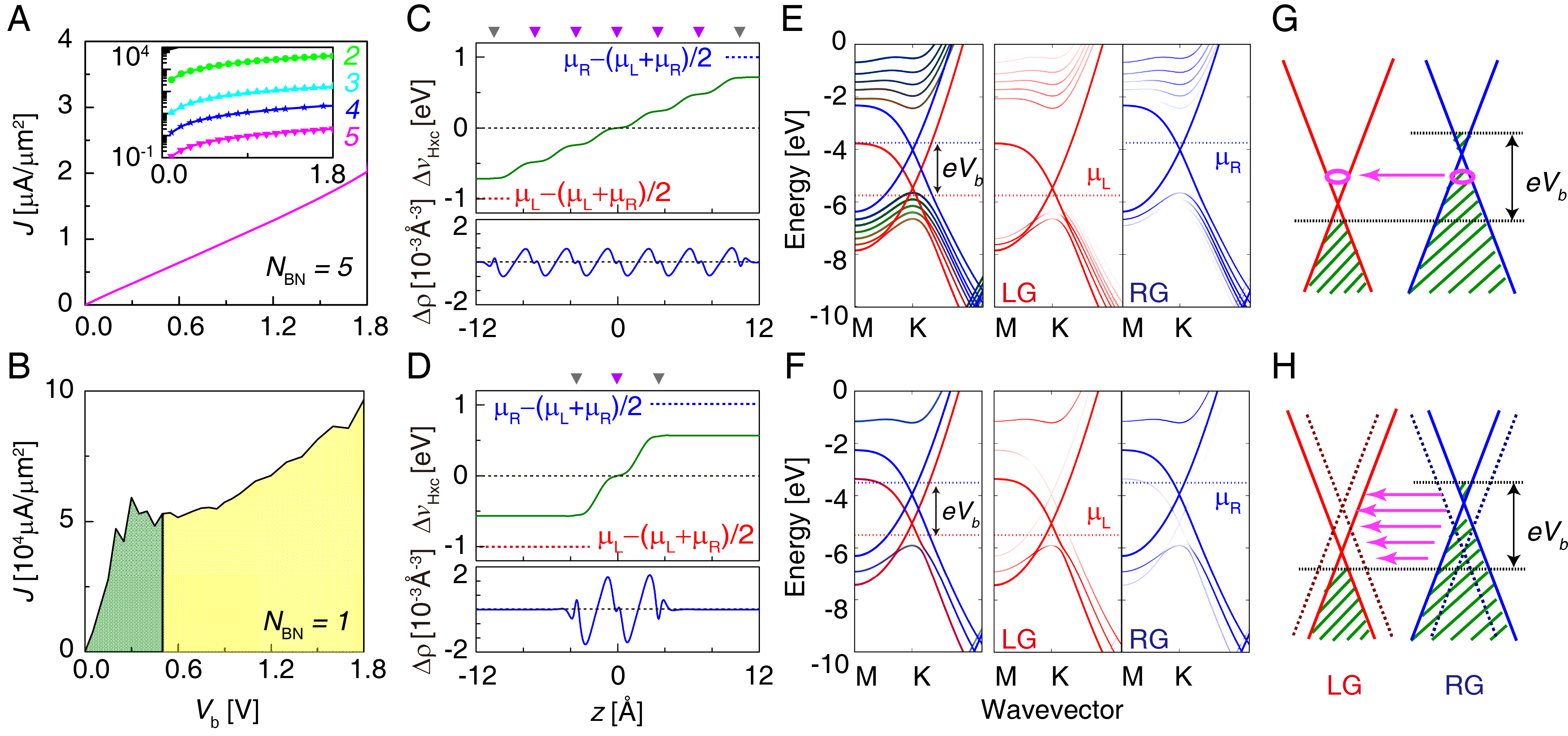
We apply MS-DFT to study 2D vdW heterostructures composed of a single- or multi-layer hBN sandwiched between graphene electrodes, a prototype configuration for the experimental realization of vertical 2D tunneling transistors and where strong NDR characteristics were observed Britnell2013 . We emphasize again that the single-layer graphene electrode case cannot be straightfowardly treated within the conventional NEGF method. Instead, for the semi-infinite graphite electrode case, we confirmed that MS-DFT reproduces the finite-bias electronic structure calculated within NEGF (see SI Appendix, Section B). Moving on the single-layer graphene electrode cases with the number of hBN layers (NBN) varying from one to five, we obtain linear characteristics for and an exponential current decrease with the increase in the number of hBN layers with a decay rate of 0.718 Å-1 (Fig. 2A). On the other hand, for the case of NBN = 1, we observe a nonlinear current density-bias voltage behavior (Fig. 2B) characterized by an NDR peak at V and a linear current increase at higher voltages.
The notable differences in the characteristics of the and cases can be understood by analyzing their electronic structures with the standard DFT analysis methods, which represents another practical advantage of MS-DFT over NEGF. In Fig. 2C and 2D, we show the bias-induced electron density redistribution and corresponding at V for the cases of and , respectively. For , the offset between left-graphene (LG) and right-graphene (RG) is significantly reduced from that which corresponds to the applied bias (2.0 eV) to 1.45 eV, reflecting the quantum capacitance of graphene or low density of states (DOS) near the graphene Dirac point Luryi1988 ; John2004 ; Fang2007 . For , the offset of LG and RG is even further reduced to 1.1 eV. The corresponding -induced shown together indicates that the amount of interfacial charge transfer in the case is larger than in the counterpart, which can be understood by the fact the drop per hBN layer in the former should be larger than that in the latter. Projecting the band structures to the LG and RG electrodes as shown in Fig. 2E and 2F also highlights another key distinction between the two cases in that there is no direct hybridization between LG and RG in the case (only up to second interfacial hBN layer bands are projected onto the graphene bands), the case of exhibits clear traces of LG Dirac cone on the RG band and vice versa (see also SI Appendix, Section C).
Identifying the direct hybridization between the LG and RG states in the case (Fig. 2H) and no hybridization in the counterparts (Fig. 2G), we now have a basis to understand their distinctively different characteristics. The cases correspond to the regime where the standard semiclassical treatment, which views the hBN layers as a simple tunnel barrier Britnell2012_NL ; Britnell2012_SC , is valid. Here, linearly increase with due to the fact that, given the constraint of energy and momentum conservation, tunneling between two shifted graphene Dirac cones at a finite can occur only for a single ring of points and the circumference of these rings linearly increases with (Fig. 2G) Feenstra2012 ; Zhao2013 . While these semiclassical arguments have been successfully employed to explain several features observed in experiments including the NDR behavior Brey2014 ; Barrera2014 ; Barrera2015 ; Greenaway2015 ; Amorim2016 , atomistic details of hBN and/or graphene are yet to be included. On the other hand, the direct hybridization between LG and RG states, which could be captured thanks to the first-principles nature of our approach, indicates that the case is a situation where the details of the potential barrier is important, by opening up transmission eigenchannels that were forbidden within the semiclassical picture (Fig. 2H).
III.2 The effect of atomic defects in hBN on NDR
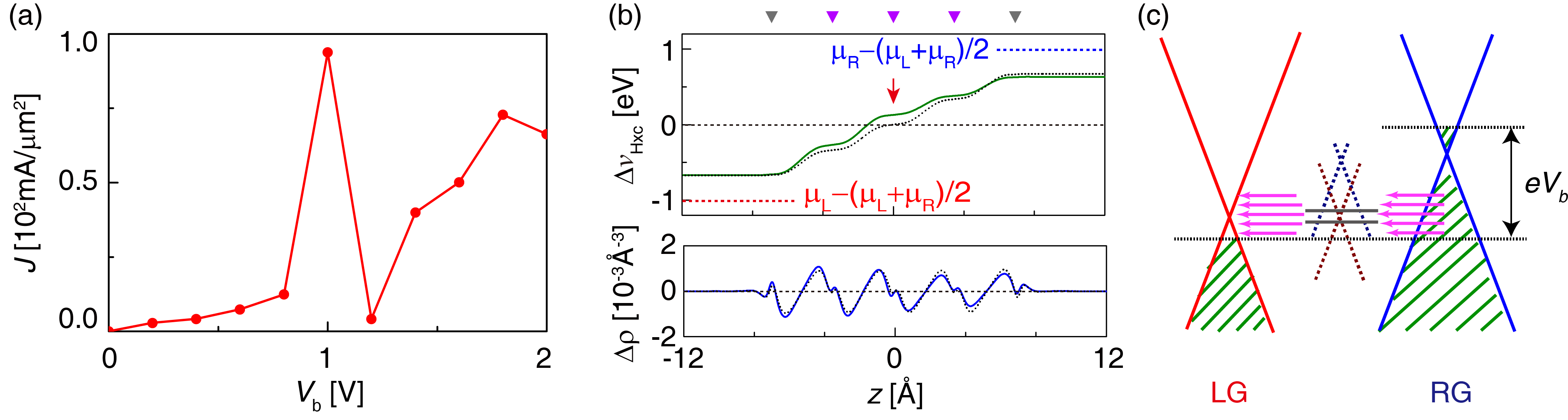
We next show that the inclusion of atomic defects indeed produces an NDR behavior for few-layer hBN junctions as observed in experiments, demonstrating the capability of our scheme to provide atomistic characterizations of disorder models only phenomenologically introduced in previous semiclassical studies Feenstra2012 ; Zhao2013 ; Britnell2013 . Specifically, we considered a case and introduced into a central hBN layer a carbon atom substituting a nitrogen atom (CN), which is known to be the most preferable defect type for hBN Azevedo2007 . Compared with the pristine case, the characteristics shown in Fig. 3A exhibit not only notably increased currents but also a more pronounced NDR peak at V. Observing the and curves at V shown in Fig. 3B, we find that the p-type polarity of CN defect states (see SI Appendix, Fig. S3) results in a bigger drop on the drain LG side than the source RG side by 0.18 eV. Correspondingly, we observe a bigger on the former than that on the latter. We thus propose that the hybridization between LG and RG states mediated by defect states, as schematically shown in Fig. 3C, is the atomistic origin of NDR in realistic situations.
III.3 The electronic origins of NDR and linear current increase
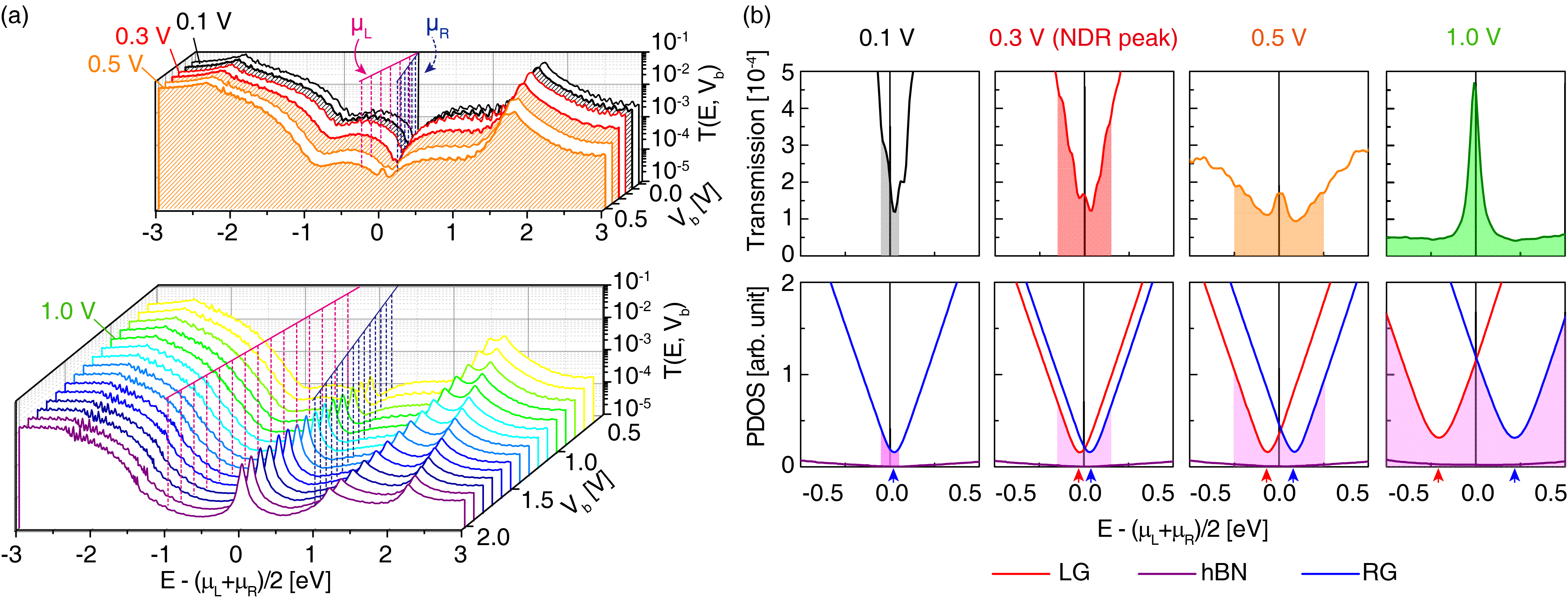
We finally examine the mechanisms of nonlinear characteristics of the single-layer hBN channel case in detail (Fig. 2 lower panels). In the Fig. 4A upper panel, we show the development of transmission functions with increasing for the low- regime where a NDR arises, and in Fig. 4B reproduced the low-bias at V (below the NDR peak), 0.3 V (NDR peak), and 0.5 V (above the NDR peak), together with the corresponding DOS projected onto the LG and RG electrodes. Most notably, due to the above-described LG-RG hybridizations, we observe that the shift of LG and RG Dirac cones is not proportional to and the shape of shows a strongly nonlinear behavior. Specifically, up to V, the shift between LG and RG Dirac points () minimally increases to 0.06 eV and concurrently more or less preserves its zero-bias shape. However, as additionally increases from 0.3 V to 0.5 V, abruptly jumps to 0.14 eV and at the same time collapses. Quantitatively, the slope of at the boundary of bias window (shaded area in Fig. 4B) decreases from 0.005 eV-1 at V to 0.002 eV-1 at V and to 0.0006 eV-1 at V.
Albeit the NDR peaks observed in experiments could be approximately accommodated within the Bardeen transfer Hamiltonian treatment through the scattering potential or finite coherence models Feenstra2012 ; Zhao2013 ; Britnell2013 , none of the semiclassical approaches could account for the high-bias linear increase in the measured characteristics. Being a first-principles approach, MS-DFT indeed successfully produces the linear background current both in the (Fig. 2B) and defective (Fig. 3A) cases. Observing the development of at the bias regime V in the case (Fig. 4A bottom panel), we find that the linear background current originates from the growth in the transmission peak at that has already emerged at V (Fig. 4B upper panel). This transmission peak was precisely the origin of the linear current increase for the pristine cases; namely, our results show that the hybridization between the LG and RG states in the low regime (Fig. 2H) is eventually broken as one increases and the system then switches to a regime where only a single ring of points contributes to the tunneling current (Fig. 2G). We thus find that the tunneling mechanisms at low and high compete with each other and the transition between the two will sensitively depend on the atomistic details of hBN barriers, demonstrating the necessity of a first-principle approach to describe the finite-bias quantum transport in 2D vdW heterojunctions.
IV Conclusions
In summary, we established a novel viewpoint that maps a quantum transport process to a multi-space (from drain to source) “excitation” within the micro-canonical picture. While the viewpoint could be beneficial in a more general context, it particularly allows one to develop a first-principles computational approach based on the constrained-search DFT procedure. The resulting MS-DFT allows stable numerical calculations of quantum transport phenomena due to its variational nature, and we applied it to 2D vertical heterostructure transistors. Focusing on the single-layer graphene electrode case, which so far could not be treated in a first-principles manner, we showed that the low- NDR behavior arises because of the direct or defect-mediated hybridizations between two graphene electrode states. Upon further increasing , it was shown that the 2D heterostructure moves into a simple tunneling regime, where one obtains a linear background current. The highly nonlinear characteristics could not be simultaneously captured in previous semiclassical treatments, which emphasizes the necessity of adopting a first-principles approach to describe 2D vdW heterostructure transistors. The novel atomistic insights obtained here demonstrate that the MS-DFT formalism will make valuable contributions to the development of next-generation devices.
Methods.
We adopted the local density approximation Ceperley1980 , Troullier-Martins-type norm-conserving pseudopotentials Troullier1991 , and numerical atomic orbital basis sets of double--plus-polarization quality defined with the confinement energy of 100 meV. The 300 Ry of real-space meshgrid cutoff energy and Monkhorst-Pack k-point grid were chosen for pristine junction cases where unit cell models are adopted. Single atomic defect CN within supercell hBN, which translates into the defect density of 7.63 × 10¹³/cm2, and Monkhorst-Pack k-point grid were chosen with the inclusion of atomic defect. In calculating , the energy was scanned from to eV around with 0.01 eV step.
Author contributions.
Y.-H.K. oversaw the project and developed the MS-DFT formalism. H.S.K. implemented the method and carried out calculations. Y.-H.K. and H.S.K. analyzed the computational results together and co-wrote the manuscript.
Acknowledgements.
This research was supported by the Basic Research Program (NRF-2017R1A2B3009872 and 2017R1A6A3A01011052), the Global Frontier Program (2013M3A6B1078881), and the Nano·Material Technology Development Program (NRF-2016M3A7B4024133) of the National Research Foundation funded by the Ministry of Science, ICT, and Future Planning of Korea. Computational resources were provided by the KISTI Supercomputing Center (KSC-2016-C3-0076 and KSC-2017-C3-0085).References
- [1] Datta S (2005) Quantum Transport: Atom to Transistor. (Cambridge University Press, Cambridge, UK).
- [2] Di Ventra M (2008) Electrical Transport in Nanoscale Systems. (Cambridge University Press, Cambridge, UK).
- [3] Britnell L, et al. (2012) Field-effect tunneling transistor based on vertical graphene heterostructures. Science 335(6071):947–950.
- [4] Britnell L, et al. (2013) Resonant tunnelling and negative differential conductance in graphene transistors. Nat Commun 4:1794.
- [5] Jena D (2013) Tunneling transistors based on graphene and 2-d crystals. Proc IEEE 101(7):1585–1602.
- [6] Li MY, Chen CH, Shi Y, Li LJ (2016) Heterostructures based on two-dimensional layered materials and their potential applications. Mater Today 19(6):322–335.
- [7] Iannaccone G, Bonaccorso F, Colombo L, Fiori G (2018) Quantum engineering of transistors based on 2d materials heterostructures. Nat Nano 13(3):183.
- [8] Mak KF, Sfeir MY, Misewich JA, Heinz TF (2010) The evolution of electronic structure in few-layer graphene revealed by optical spectroscopy. Proc Natl Acad Sci U S A 107(34):14999–15004.
- [9] Kang S, et al. (2016) Effects of electrode layer band structure on the performance of multilayer graphene-hBN-graphene interlayer tunnel field effect transistors. Nano Lett 16(8):4975–4981.
- [10] Bardeen J (1961) Tunnelling from a many-particle point of view. Phys Rev Lett 6(2):57–59.
- [11] Tersoff J, Hamann DR (1985) Theory of the scanning tunneling microscope. Phys Rev B 31(2):805–813.
- [12] Feenstra RM, Jena D, Gu G (2012) Single-particle tunneling in doped graphene-insulator-graphene junctions. J Appl Phys 111(4):043711.
- [13] Zhao P, Feenstra RM, Gu G, Jena D (2013) Symfet: A proposed symmetric graphene tunneling field-effect transistor. IEEE Trans Electron Dev 60(3):951–957.
- [14] Campbell PM, Tarasov A, Joiner CA, Ready WJ, Vogel EM (2015) Enhanced resonant tunneling in symmetric 2d semiconductor vertical heterostructure transistors. ACS Nano 9(5):5000–5008.
- [15] Di Ventra M, Todorov TN (2004) Transport in nanoscale systems: the microcanonical versus grand-canonical picture. J Phys Condens Matter 16(45):8025.
- [16] Bushong N, Sai N, Di Ventra M (2005) Approach to steady-state transport in nanoscale conductors. Nano Lett 5(12):2569–2572.
- [17] Levy M, Nagy Á (1999) Variational density-functional theory for an individual excited state. Phys Rev Lett 83(21):4361–4364.
- [18] Ayers PW, Levy M (2009) Time-independent (static) density-functional theories for pure excited states: Extensions and unification. Phys Rev A 80.
- [19] G’́orling A (1999) Density-functional theory beyond the hohenberg-kohn theorem. Phys Rev A 59:3359–3374.
- [20] Kim YH, Jang SS, Jang YH, Goddard WA (2005) First-principles study of the switching mechanism of [2]catenane molecular electronic devices. Phys Rev Lett 94(15):156801.
- [21] Kim YH, Tahir-Kheli J, Schultz PA, Goddard WA (2006) First-principles approach to the charge-transport characteristics of monolayer molecular-electronics devices: Application to hexanedithiolate devices. Phys Rev B 73(23):235419.
- [22] Marzari N, Mostofi AA, Yates JR, Souza I, Vanderbilt D (2012) Maximally localized wannier functions: Theory and applications. Rev Mod Phys 84(4):1419.
- [23] Soler JM, et al. (2002) The siesta method for ab initio order-n materials simulation. J Phys Condens Matter 14(11):2745.
- [24] Taylor J, Guo H, Wang J (2001) Ab initio modeling of quantum transport properties of molecular electronic devices. Phys Rev B 63(24):1–13.
- [25] Brandbyge M, Mozos JL, Ordejón P, Taylor J, Stokbro K (2002) Density-functional method for nonequilibrium electron transport. Phys Rev B 65(16):165401.
- [26] Ke SH, Baranger HU, Yang W (2004) Electron transport through molecules: Self-consistent and non-self-consistent approaches. Phys Rev B 70(8):085410.
- [27] Rocha A, Sanvito S (2004) Asymmetric I-V characteristics and magnetoresistance in magnetic point contacts. Phys Rev B 70(9):094406.
- [28] Luryi S (1988) Quantum capacitance devices. Appl Phys Lett 52(6):501–503.
- [29] John DL, Castro LC, Pulfrey DL (2004) Quantum capacitance in nanoscale device modeling. J Appl Phys 96(9):5180–5184.
- [30] Fang T, Konar A, Xing H, Jena D (2007) Carrier statistics and quantum capacitance of graphene sheets and ribbons. Appl Phys Lett 91(9):092109.
- [31] Britnell L, et al. (2012) Electron tunneling through ultrathin boron nitride crystalline barriers. Nano Lett 12(3):1707–1710.
- [32] Brey L (2014) Coherent tunneling and negative differential conductivity in a graphene/-bn/graphene heterostructure. Phys Rev Applied 2(1):014003.
- [33] de la Barrera SC, Gao Q, Feenstra RM (2014) Theory of graphene-insulator-graphene tunnel junctions. J Vac Sci Technol B 32(4):04E101.
- [34] de la Barrera SC, Feenstra RM (2015) Theory of resonant tunneling in bilayer-graphene/hexagonal-boron-nitride heterostructures. Appl Phys Lett 106(9):093115.
- [35] Greenaway M, et al. (2015) Resonant tunnelling between the chiral landau states of twisted graphene lattices. Nat Phys 11(12):1057.
- [36] Amorim B, Ribeiro RM, Peres NMR (2016) Multiple negative differential conductance regions and inelastic phonon assisted tunneling in graphene-bn-graphene structures. Phys Rev B 93(23):235403.
- [37] Azevedo S, Kaschny JR, de Castilho CMC, de Brito Mota F (2007) A theoretical investigation of defects in a boron nitride monolayer. Nanotechnology 18(49):495707.
- [38] Ceperley DM, Alder BJ (1980) Ground state of the electron gas by a stochastic method. Phys Rev Lett 45(7):566–569.
- [39] Troullier N, Martins JL (1991) Efficient pseudopotentials for plane-wave calculations. Phys Rev B 43(3):1993–2006.